EP1114448B1 - Verfahren zur herstellung einer halbleitervorrichtung - Google Patents
Verfahren zur herstellung einer halbleitervorrichtung Download PDFInfo
- Publication number
- EP1114448B1 EP1114448B1 EP00927187A EP00927187A EP1114448B1 EP 1114448 B1 EP1114448 B1 EP 1114448B1 EP 00927187 A EP00927187 A EP 00927187A EP 00927187 A EP00927187 A EP 00927187A EP 1114448 B1 EP1114448 B1 EP 1114448B1
- Authority
- EP
- European Patent Office
- Prior art keywords
- silicon
- phase
- area
- titanium
- titanium silicide
- Prior art date
- Legal status (The legal status is an assumption and is not a legal conclusion. Google has not performed a legal analysis and makes no representation as to the accuracy of the status listed.)
- Expired - Lifetime
Links
Images



Classifications
-
- H—ELECTRICITY
- H10—SEMICONDUCTOR DEVICES; ELECTRIC SOLID-STATE DEVICES NOT OTHERWISE PROVIDED FOR
- H10D—INORGANIC ELECTRIC SEMICONDUCTOR DEVICES
- H10D30/00—Field-effect transistors [FET]
- H10D30/60—Insulated-gate field-effect transistors [IGFET]
-
- H—ELECTRICITY
- H10—SEMICONDUCTOR DEVICES; ELECTRIC SOLID-STATE DEVICES NOT OTHERWISE PROVIDED FOR
- H10D—INORGANIC ELECTRIC SEMICONDUCTOR DEVICES
- H10D64/00—Electrodes of devices having potential barriers
- H10D64/01—Manufacture or treatment
- H10D64/011—Manufacture or treatment of electrodes ohmically coupled to a semiconductor
- H10D64/0111—Manufacture or treatment of electrodes ohmically coupled to a semiconductor to Group IV semiconductors
- H10D64/0112—Manufacture or treatment of electrodes ohmically coupled to a semiconductor to Group IV semiconductors using conductive layers comprising silicides
-
- H—ELECTRICITY
- H10—SEMICONDUCTOR DEVICES; ELECTRIC SOLID-STATE DEVICES NOT OTHERWISE PROVIDED FOR
- H10D—INORGANIC ELECTRIC SEMICONDUCTOR DEVICES
- H10D64/00—Electrodes of devices having potential barriers
- H10D64/01—Manufacture or treatment
- H10D64/031—Manufacture or treatment of data-storage electrodes
- H10D64/035—Manufacture or treatment of data-storage electrodes comprising conductor-insulator-conductor-insulator-semiconductor structures
Definitions
- the invention relates to a method of manufacturing a semiconductor device, in particular an integrated circuit, in a superficial silicon layer of a wafer, which superficial silicon layer is provided at a surface with a component comprising an area of silicon, which area is at least substantially marked off by insulating material and covered with a high-resistivity phase of titanium silicide, whereupon the wafer is subjected to a phase-transformation anneal to transform the high-resistivity phase of titanium silicide into a low-resistivity phase of titanium silicide.
- Titanium silicide has become the most widely applied silicide in the VLSI industry for self-aligned silicide applications, which aim at reducing sheet and contact resistances of circuits.
- titanium silicide exists as either an orthorhombic base-centered phase having 12 atoms per unit cell and a resistivity of about 60-100 ⁇ cm, which high-resistivity phase is also known as the C49 phase of titanium silicide, or as a more thermodynamically-favored orthorhombic phase having 24 atoms per unit cell and a resistivity of about 12-20 ⁇ cm, which low-resistivity phase is also known as the C54 phase of titanium silicide.
- the less-desirable, high-resistivity (C49) phase of titanium silicide is formed first.
- a high-temperature phase-transformation anneal is needed.
- a method of manufacturing a semiconductor device of the kind mentioned in the opening paragraph is known from Japanese Patent Application JP-A-8-008211 .
- a surface of a monocrystalline silicon wafer is provided with a MOS transistor having a polycrystalline or amorphous silicon gate, a source and a drain, which elements each provide part of an exposed area of silicon, which area of silicon is at least substantially marked off by insulating material provided by oxide or nitride sidewall spacers and oxide field insulating regions (not shown in figures).
- the wafer is subsequently provided with a polycrystalline or amorphous silicon layer having a thickness in the order of 10 nm, which silicon layer is topped by a titanium layer having a thickness of 30 to 40 nm or more.
- the wafer is subjected to a silicide-formation anneal in order to form the high-resistivity (C49) phase of titanium silicide at the entire surface of the wafer.
- the silicide formation anneal is carried out until the silicon layer above the insulating material as well as the titanium layer above the gate, the drain and the source is converted over its entire thickness. Parts of the titanium layer left behind at the surface of the wafer after the silicide formation anneal are removed by means of selective etching.
- the wafer After removal of the titanium layer parts, the wafer is subjected to the phase-transformation anneal, in order to transform the high-resistivity (C49) phase of titanium silicide into the low-resistivity (C54) phase of titanium silicide.
- the entire surface of the wafer is then etched back in order to remove the low-resistivity (C54) phase of titanium silicide present on the insulating material. During this etch-back process, also part of the low-resistivity (C54) phase of titanium silicide present on the gate, the source and the drain is removed.
- the entire surface of the wafer is provided with the high-resistivity (C49) phase of titanium silicide in order to make the subsequent transformation into the low-resistivity (C54) phase of titanium silicide independent of device line-width. It is thought that the C49 into C54 phase transformation of titanium silicide is becoming increasingly difficult as the device line-width continues to be scaled down.
- a disadvantage of the known method is that ultimately the entire surface of the wafer is covered with the low-resistivity (C54) phase of titanium silicide.
- An etch-back operation is thus needed to re-expose the insulating material provided by the oxide or nitride sidewall spacers and the oxide field insulating regions.
- This etch-back operation represents an additional process step, which is rather critical. If the etch-back operation is stopped too early, titanium silicide remainders are left behind on e.g. the oxide or nitride sidewall spacers, which remainders may give rise to serious leakage currents due to a problem commonly referred to as over-spacer bridging. On the other hand, if the etch-back operation is carried on too long, the sheet and contact resistances of the MOS transistor are adversely affected.
- EP 0 812 009 discloses a method of forming silicided narrow polysilicon lines.
- a prior gas implant makes the transformation from C49 to C54 easier.
- the transformation is performed by RTA.
- this object is achieved in that the transformation of the high-resistivity phase of titanium silicide into the low-resistivity phase of titanium silicide is promoted by providing the area with an extension of silicon, which extension is at least substantially marked off by insulating material and covered with the high-resistivity phase of titanium silicide, the extension being relatively large compared to the area.
- the invention is based inter alia on the insight, that the transformation of the high-resistivity (C49) phase of titanium silicide into the low-resistivity (C54) phase of titanium silicide is dependent on surface area rather than line-width.
- the invention is illustrated hereinafter on the basis of a component in the form of a process control module, it will be evident to those skilled in the art that the invention may also be advantageously applied for a single active circuit device such as, for example, a field-effect transistor, a bipolar transistor or a floating gate transistor, or for a CMOS or BICMOS integrated circuit known per se.
- a single active circuit device such as, for example, a field-effect transistor, a bipolar transistor or a floating gate transistor, or for a CMOS or BICMOS integrated circuit known per se.
- the process control module shown in a diagrammatic top view in Fig. 1 represents a memory containing storage cells, which are arranged in an array of 4 rows by 4 columns. It will be evident that the number of rows and columns in general is much larger than 4.
- the storage cells share electrical connections with all the other storage cells in their rows and columns and are situated at intersections of word lines 1 and bit lines 2.
- Each one of the storage cells comprises a field-effect transistor having a floating gate, a control gate, a source and a drain, which transistor is also referred to as floating gate transistor.
- the word lines 1 each provide for the control gates of the floating gate transistors situated in a common row and are driven by an address decoder (not shown).
- the bit lines 2 are each connected with the drains of the floating gate transistors situated in a common column and are connected with an address decoder and/or read circuit (not shown).
- the process control module also comprises source lines 3, which are grounded in the present example. Each of the source lines 3 connects the sources of the floating gate transistors with one another, which sources are situated in one or two adjacent common rows.
- the source lines 3 are provided with a common extension 4, which is relatively large compared to each of the source lines 3.
- the common extension 4 serves to promote the C49 into C54 phase transformation of titanium silicide on each of the source lines 3 during the self-aligned silicide process, also referred to as salicide process, to which the process control module is subjected during its manufacture.
- the extension 4 is connected to all source lines 3 of the process control module. This is possible, because the source lines 3 are all grounded. It will be evident, however, that it is also possible to provide each of the source lines 3 with a separate extension 4, or to provide, for example, one or more of the word lines 1 with an extension.
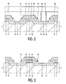
- Fig. 2 shows a diagrammatic cross-sectional view of a floating gate transistor taken along line A-A in Fig. 1 , similar elements being indicated by similar reference numerals.
- the floating gate transistor is disposed on a surface 5 of a superficial silicon layer 6 of a first conductivity type, in the present example the p-type, which superficial silicon layer 6 is part of a wafer 7, in the present example a mono-crystalline silicon wafer.
- the floating gate transistor has a floating gate 8 composed of, for example, n-type polycrystalline silicon, which is situated between an overlapping control gate 9 composed of, for example, n-type polycrystalline silicon and a channel 10, which is situated in the superficial silicon layer 6 and extends between a source 11 and a drain 12 of a second, opposite conductivity type, in the present example the n-type.
- the floating gate 8 is insulated from the superficial silicon layer 6 by a floating gate dielectric 13 and from the overlapping control gate 9 by an inter-gate dielectric 14.
- the control gate 9 is provided with sidewall spacers 15 composed of, for example, silicon oxide or silicon nitride.
- silicon regions 16, 17 and 18, which silicon regions are provided by respectively the control gate 9, the source 11 and the drain 12, are covered with a low-resistivity (C54) phase 19 of titanium silicide.
- the floating gate transistor is covered with a dielectric layer 20 composed of, for example, BPSG (boro-phospho-silicate glass) on top of TEOS (tetra-ethyl-ortho-silicate), which dielectric layer 20 is provided with a contact hole 21 to allow one of the bit lines 2 to contact the drain 12 of the floating gate transistor, thereby giving rise to a drain contact 22 (see also Fig. 1 ).
- Figs. 3 to 6 show in diagrammatic cross-sectional views successive stages in the manufacture of the floating gate transistor of Fig. 2 the source 11 of which is connected with the extension 4 via one of the source lines 3 of the process control module.
- the manufacture starts with the wafer 7 ( Fig. 3 ), in the present example a monocrystalline silicon wafer, comprising the superficial silicon layer 6 of a first conductivity type, in the present example the p-type.
- the superficial silicon layer 6 is provided with the oxide field insulating regions (not shown) in a usual way by means of LOCOS (LOCal Oxidation of Silicon) or STI (Shallow Trench Isolation), which oxide field insulating regions are at least partly recessed in the superficial silicon layer 6 and define an active region therein.
- LOCOS LOCOS
- STI Shallow Trench Isolation
- a dielectric material with a dielectric constant higher than that of silicon oxide such as tantalum oxide, aluminium oxide or silicon nitride, may be applied.
- a layer of, for example, polycrystalline silicon doped with, for example, phosphorus is applied, which layer is subsequently patterned in a usual photolithographic way to provide the floating gate 8.
- amorphous silicon or Si x Ge 1-x may be used, with x representing the fraction of silicon lying in the range between about 0.6 and 1.
- the source 11 and the drain 12 of the second, opposite conductivity type are formed on opposite sides of the floating gate 8 by means of a self-aligned implantation of a dose of, for example, phosphorus or arsenic.
- the floating gate 8 is covered with a further insulating layer composed of, for example, silicon oxide, providing the inter-gate dielectric 14.
- silicon oxide silicon oxide
- SiON silicon oxynitride
- ONO sandwich of silicon oxide and silicon nitride
- dielectric material with a dielectric constant significantly higher than that of silicon oxide such as tantalum oxide, aluminum oxide or silicon nitride may be applied.
- a layer of, for example, polycrystalline silicon doped with, for example, phosphorus is applied, which layer is subsequently patterned in a usual photolithographic way to provide the overlapping control gate 9.
- amorphous silicon or Si x Ge 1-x may be used, with x representing the fraction of silicon lying in the range between about 0.6 and 1.
- the sidewalls of the control gate 9 are subsequently provided with sidewall spacers 15 in a known way, for example, by means of deposition and anisotropic etch-back of a silicon oxide or a silicon nitride layer. The resulting situation is shown in Fig. 3 .
- the floating gate transistor comprises exposed silicon regions 16, 17 and 18, which exposed silicon regions are provided by, respectively, the control gate 9, the source 11 and the drain 12. Each of the exposed silicon regions 16, 17 and 18 is part of an exposed area of silicon, which exposed area of silicon is at least substantially marked off by insulating material.
- the exposed silicon region 16 is part of one of the word lines 1 (see Fig. 1 ).
- the word lines 1 each represent an exposed area of silicon, in the present example of polycrystalline silicon, which exposed area of silicon is at least substantially marked off by the insulating material provided by the nitride or oxide sidewall spacers 15 of the floating gate transistors situated in a common row and by oxide field insulating regions (not shown).
- the exposed silicon region 18 represents on its own (see Fig.
- an exposed area of silicon in the present example of mono-crystalline silicon, on its own, which exposed area of silicon is at least substantially marked off by the insulating material provided by the nitride or oxide sidewall spacers 15 of the floating gate transistors situated in two adjacent common rows and by oxide field insulating regions (not shown).
- the exposed silicon region 17 is part of one of the source lines 3 (see Fig. 1 ).
- the source lines 3 each represent an exposed area of silicon, in the present example monocrystalline silicon, which exposed area of silicon is at least substantially marked off by the insulating material provided by the nitride or oxide sidewall spacers 15 of the floating gate transistors situated in one or two adjacent common rows and by oxide field insulating regions (not shown), and is provided with the common extension 4 of silicon, in the present example monocrystalline silicon.
- the common extension 4, which is at least substantially marked off by the insulating material provided by oxide field insulating regions (not shown), is applied in order to promote the C49 into C54 phase transformation of titanium silicide on each of the source lines 3 and is relatively large compared to each of the source lines 3.
- the wafer 7 is now subjected to a self-aligned silicide process, also referred to as salicide process, in which process each exposed area of silicon and, hence, each of the exposed silicon regions 16, 17 and 18 is provided with a high-resistivity (C49) phase 23 of titanium silicide (see Fig. 5 ), which high-resistivity phase 23 needs to be transformed into the low-resistivity (C54) phase 19 of titanium silicide at a later stage in the same process (see Fig. 6 ).
- C49 high-resistivity
- C54 low-resistivity
- the successive stages of this salicide process will now be described in more detail with respect to the exposed silicon regions 16, 17 and 18 of the floating gate transistor. It will be evident, however, that each exposed area of silicon of the process control module of Fig. 1 and, hence, each of the source lines 3, which are provided with the extension 4 for the above-mentioned reason, passes through the same succession of stages.
- the salicide process usually starts with a deoxidation step to remove oxide remainders from the exposed silicon regions 16, 17 and 18 ( Fig. 3 ). These oxide remainders may have been formed as a result of exposure to air (native oxide) or as a result of masked etching of a layer composed of, for example, TEOS (tetra-ethyl-ortho-silicate), which can be used to protect certain silicon regions against silicidation during the above mentioned salicide process. Removal of these oxide remainders may be carried out by means of wet chemical etching using, for example, a solution containing 1% hydrofluoric acid (HF).
- HF hydrofluoric acid
- a titanium-containing layer 24 is applied to the wafer 7.
- the titanium-containing layer 24 may be applied as a single layer of titanium by means of plasma-enhanced chemical vapor deposition (PECVD) at a temperature between about 400°C and 700°C, whereby the exposed silicon regions 16, 17 and 18 are immediately provided with the high-resistivity (C49) phase of titanium silicide, or by means of physical vapor deposition at a relatively low temperature, whereby the exposed silicon regions 16, 17 and 18 are provided with titanium, which is to be converted into the high-resistivity (C49) phase of titanium silicide at a later stage in the process, as described below.
- PECVD plasma-enhanced chemical vapor deposition
- the titanium-containing layer 24 is advantageously applied as a double-layer consisting of a first sub-layer 25 of titanium with a second sub-layer 26 of titanium nitride on top, which second sub-layer 26 acts as a capping layer to avoid e.g. adverse oxidation of the first sub-layer 25 of titanium.
- the first sub-layer 25 and the second sub-layer 26 may be applied by means of physical vapor deposition in a thickness of, for example, about 30 nm and about 25 nm, respectively.
- the wafer 7 is subjected to a silicide formation anneal in order to convert the first sub-layer 25 of titanium, at the silicon regions 16, 17 and 18, to the high-resistivity (C49) phase 23 of titanium silicide over at least part of its thickness.
- a silicide formation anneal in order to convert the first sub-layer 25 of titanium, at the silicon regions 16, 17 and 18, to the high-resistivity (C49) phase 23 of titanium silicide over at least part of its thickness.
- the silicide formation anneal is carried out in nitrogen (N 2 ) or a nitrogen-based atmosphere, or in an inert-gas atmosphere of, for example, argon (Ar).
- the silicide formation anneal may be carried out as a conventional furnace anneal, it is advantageously carried out as a rapid thermal anneal (RTA) in order to lower the thermal budget of the wafer 7.
- RTA rapid thermal anneal
- a lower thermal budget at this stage of the salicide process is favorable, because it counteracts the occurrence of parasitic effects such as, for example, lateral growth of titanium silicide over the sidewall spacers 15, which is a problem known as over-spacer bridging.
- the rapid thermal anneal may be carried out in, for example, nitrogen (N 2 ) at a temperature of, for example, about 730°C during a time of, for example, about 20 seconds.
- the high-resistivity phase 23 of titanium silicide is formed on top of each area of silicon, which area is at least substantially marked off by the insulating material provided by the oxide or nitride sidewall spacers 15 and the oxide field insulating regions (not shown), and, hence, on top of each of the source lines 3 and the extension 4 with which each of the source lines 3 is connected.
- titanium silicide is not formed on top of the insulating material provided by the oxide or nitride sidewall spacers 15 and the oxide field insulating regions (not shown)
- titanium-containing material not converted into the high-resistivity phase 23 of titanium silicide needs to be removed, which titanium-containing material comprises titanium 27 and titanium nitride 28, present on the insulating material provided by the oxide or nitride sidewall spacers and the oxide field insulating regions, and titanium nitride 29 present on the high-resistivity phase 23 of titanium silicide.
- the titanium 27 present on the insulating material may comprise small amounts of oxygen and silicon if silicon oxide is applied as an insulating material or small amounts of oxygen, nitrogen and silicon if silicon nitride is applied as an insulating material.
- the titanium 27 and the titanium nitride 28,29 may be removed after phase transformation of the high-resistivity phase 23 of titanium silicide into the low-resistivity phase 19 of titanium silicide, but are preferably removed before said phase transformation.
- This can be done by means of selective wet etching using, for example, a so-called standard clean 1 (SC1) chemistry at, for example, about 30°C during a time of, for example, about 20 minutes, which SC1 chemistry involves a mixture of ammonium hydroxide (NH 4 OH): hydrogen peroxide (H 2 O 2 ): water (H 2 O) in a ratio of, for example, about 1:2:7.
- SC1 chemistry involves a mixture of ammonium hydroxide (NH 4 OH): hydrogen peroxide (H 2 O 2 ): water (H 2 O) in a ratio of, for example, about 1:2:7.
- the wafer 7 is subjected to a phase transformation anneal in order to transform the high-resistivity (C49) phase 23 at the silicon regions 16, 17 and 18 into the low-resistivity (C54) phase 19 of titanium silicide ( Fig. 6 ).
- the phase transformation anneal may be carried out as a conventional furnace anneal, it is advantageously carried out as a rapid thermal anneal (RTA) in order to lower the thermal budget of the wafer 7.
- RTA rapid thermal anneal
- a lower thermal budget at this stage of the salicide process is favorable, because it counteracts the occurrence of parasitic effects such as, for example, dopant redistribution between doped areas of silicon and the titanium silicide with which these areas are in contact.
- the rapid thermal anneal may be carried out in, for example, nitrogen (N 2 ) at a temperature of, for example, about 900°C during a time of, for example, about 20 seconds.
- the high-resistivity (C49) phase 23 of titanium silicide is transformed into the low-resistivity (C54) phase 19 of titanium silicide at each area of silicon, which area is at least substantially marked off by the insulating material provided by the oxide or nitride sidewall spacers 15 and the oxide field insulating regions (not shown).
- the source lines 3 are provided with a relatively large extension 4, which is covered with the high-resistivity (C49) phase of titanium silicide as well.
- the dielectric layer 20 composed of, for example, BPSG (boro-phospho-silicate glass) on top of TEOS (tetra-ethyl-ortho-silicate), is applied to the wafer 7, which dielectric layer 20 is provided with the contact hole 21 to allow one of the bit lines 2 to contact the drain 12 of the floating gate transistor, thereby giving rise to the drain contact 22, the result of which is shown in Fig. 2 .
- BPSG boro-phospho-silicate glass
- TEOS tetra-ethyl-ortho-silicate
- Figs. 7 and 8 show cumulative graphs of the relationship between the phase transformation yield (Y in %) and the sheet resistance (R ⁇ in ⁇ / ⁇ ) of, respectively, a doped polycrystalline silicon area covered with titanium silicide and a doped mono-crystalline silicon area covered with titanium silicide for different extension sizes.
- the sizes of the extensions are about 18 ⁇ m 2 (circles), 32 ⁇ m 2 (squares), 50 ⁇ m 2 (crosses), 110 ⁇ m 2 (triangles) and 450 ⁇ m 2 (stars) in both graphs.
- the titanium silicide is present in a thickness of about 30 nm on each of the doped areas and the extension connected therewith, which thickness is approximately independent of the phase in which the titanium silicide is.
- a phase-transformation yield (Y) of 10% corresponds to 40 samples, a yield of 50% to 200 samples, a yield of 90% to 360 samples, and so on.
- the highest sheet resistances depicted correspond to the high-resistivity (C49) phase of titanium silicide
- the lowest sheet resistances depicted (about 2 ⁇ / ⁇ ) correspond to the low-resistivity (C54) phase of titanium silicide.
- the variation in the sheet resistances corresponding to the high-resistivity (C49) phase of titanium silicide can probably be attributed to small deviations in the stoichiometry of the high-resistivity phase.
- Figs. 7 and 8 clearly reveal that the phase-transformation yield (Y) at a given sheet resistance (R ⁇ ) increases with increasing extension size. From the design point of view, a sheet resistance of about 5 ⁇ / ⁇ is generally considered sufficiently low.
- Figs. 7 and 8 show that, in order to reach a phase transformation yield (Y) of about 95% at a sheet resistance of 5 ⁇ / ⁇ , the doped polycrystalline silicon area of 10.5 ⁇ m 2 as well as the doped mono-crystalline silicon area of 12.0 ⁇ m 2 should be provided with an extension having a size of about 50 ⁇ m 2 .
- the extension size should be about 110 ⁇ m 2 for the doped polycrystalline silicon area of 10.5 ⁇ m 2 as well as for the doped monocrystalline silicon area of 12.0 ⁇ m 2 .
- the area of silicon which is provided with an extension to promote the C49 into C54 phase transformation of titanium silicide, may comprise, for example, monocrystalline silicon, polycrystalline silicon, amorphous silicon or silicon germanium alloy, namely Si x Ge 1-x , with x, being the fraction of silicon, lying in the range between about 0.6 and 1. Because this alloy largely consists of silicon, it is regarded as silicon herein. Moreover, the silicon may be intrinsic or intentionally doped to exhibit p-type or n-type conductivity. In the embodiments described above, the extension was provided in a rectangular form.
- the wafer is a mono-crystalline wafer having a superficial silicon layer defined at a main surface of it.
- the wafer may be a silicon-on-insulator (SOI) wafer comprising a body of semiconductor material, for example silicon, which body is provided at a main surface with a layer of insulating material, for example silicon oxide or silicon nitride, which layer of insulating material is covered with a layer of silicon representing the above-mentioned superficial silicon layer.
- SOI silicon-on-insulator
Landscapes
- Electrodes Of Semiconductors (AREA)
- Internal Circuitry In Semiconductor Integrated Circuit Devices (AREA)
- Semiconductor Memories (AREA)
- Non-Volatile Memory (AREA)
- Insulated Gate Type Field-Effect Transistor (AREA)
- Thin Film Transistor (AREA)
Claims (8)
- Verfahren zur Herstellung einer Halbleitervorrichtung, insbesondere einer integrierten Schaltung, in einer Silizium-Oberflächenschicht (6) eines Wafers (5), die an einer Oberfläche (5) mit einem Bauelement umfassend ein Gebiet aus Silizium (16, 17, 18) versehen ist, das durch isolierendes Material (15) abgegrenzt ist und mit einer hochohmigen Phase des Titansilizids (19) abgedeckt ist, woraufhin der Wafer einer Phasentransformations-Wärmebehandlung unterzogen wird, um die hochohmige Phase des Titansilizids in eine niederohmige Phase des Titansilizids zu transformieren, dadurch gekennzeichnet, dass die Transformation der hochohmigen Phase des Titansilizids in die niederohmige Phase des Titansilizids durch Versehen des Gebiets (4) mit einem Erweiterungsgebiet aus Silizium gefördert wird, wobei das Erweiterungsgebiet durch isolierendes Material abgegrenzt wird und mit der hochohmigen Phase des Titansilizids abgedeckt wird, und wobei das Erweiterungsgebiet relativ groß im Vergleich mit dem Gebiet ist.
- Verfahren nach Anspruch 1, dadurch gekennzeichnet, dass die hochohmige Phase des Titansilizids, die das Gebiet und das Erweiterungsgebiet aus Silizium abdeckt, durch Aufbringen einer Titan enthaltenden Schicht, Unterwerfen des Wafers unter eine Silizidbildungs-Wärmebehandlung zur Umwandlung der Titan enthaltenden Schicht im Gebiet und im Erweiterungsgebiet in die hochohmige Phase des Titansilizids über mindestens einen Teil ihrer Dicke gebildet wird.
- Verfahren nach Anspruch 2, dadurch gekennzeichnet, dass die Titan enthaltende Schicht als Doppelschicht mit einer ersten Sub-Schicht enthaltend Titan und einer darüber liegenden zweiten Sub-Schicht enthaltend Titannitrid abgeschieden wird.
- Verfahren nach Anspruch 2 oder 3, dadurch gekennzeichnet, dass zwischen der Silizidbildungs-Wärmebehandlung und der Phasentransformations-Wärmebehandlung der Wafer einer Ätzbehandlung unterzogen wird, um jegliches Titan enthaltendes Material, das nicht in die hochohmige Phase von Titansilizid umgewandelt ist, vom isolierenden Material und vom Gebiet und dem Erweiterungsgebiet zu entfernen.
- Verfahren nach einem der Ansprüche 2 bis 4, dadurch gekennzeichnet, dass die Silizidbildungs-Wärmebehandlung als schnelle thermische Wärmebehandlung ausgeführt wird.
- Verfahren nach einem der vorstehenden Ansprüche, dadurch gekennzeichnet, dass die Phasentransformations-Wärmebehandlung als schnelle thermische Wärmebehandlung ausgeführt wird.
- Verfahren nach einem der vorstehenden Ansprüche, dadurch gekennzeichnet, dass das Bauelement als ein Prozesssteuerungsmodul auf die Oberfläche der Oberflächensiliziumschicht aufgebracht wird.
- Verfahren nach einem der Ansprüche 1 bis 6, dadurch gekennzeichnet, dass das Bauelement als ein Transistor mit Gate (9), Source (11) und Drain (12) auf die Oberfläche der Oberflächen-Siliziumschicht aufgebracht wird, wobei das Gebiet aus Silizium (6) durch mindestens eines der Elemente Gate (9), Source (11) und Drain (12) gebildet wird.
Priority Applications (1)
| Application Number | Priority Date | Filing Date | Title |
|---|---|---|---|
| EP00927187A EP1114448B1 (de) | 1999-05-27 | 2000-05-08 | Verfahren zur herstellung einer halbleitervorrichtung |
Applications Claiming Priority (4)
| Application Number | Priority Date | Filing Date | Title |
|---|---|---|---|
| EP99201693 | 1999-05-27 | ||
| EP99201693 | 1999-05-27 | ||
| EP00927187A EP1114448B1 (de) | 1999-05-27 | 2000-05-08 | Verfahren zur herstellung einer halbleitervorrichtung |
| PCT/EP2000/004221 WO2000074126A1 (en) | 1999-05-27 | 2000-05-08 | A method of manufacturing a semiconductor device |
Publications (2)
| Publication Number | Publication Date |
|---|---|
| EP1114448A1 EP1114448A1 (de) | 2001-07-11 |
| EP1114448B1 true EP1114448B1 (de) | 2008-06-25 |
Family
ID=8240248
Family Applications (1)
| Application Number | Title | Priority Date | Filing Date |
|---|---|---|---|
| EP00927187A Expired - Lifetime EP1114448B1 (de) | 1999-05-27 | 2000-05-08 | Verfahren zur herstellung einer halbleitervorrichtung |
Country Status (6)
| Country | Link |
|---|---|
| EP (1) | EP1114448B1 (de) |
| JP (1) | JP2003501801A (de) |
| KR (1) | KR100664328B1 (de) |
| DE (1) | DE60039282D1 (de) |
| TW (1) | TW466692B (de) |
| WO (1) | WO2000074126A1 (de) |
Families Citing this family (4)
| Publication number | Priority date | Publication date | Assignee | Title |
|---|---|---|---|---|
| JP2002231971A (ja) * | 2001-02-02 | 2002-08-16 | Sharp Corp | 半導体集積回路装置、その製造方法、icモジュール、icカード |
| JP2005092963A (ja) | 2003-09-16 | 2005-04-07 | Renesas Technology Corp | 不揮発性記憶装置 |
| JP2005311300A (ja) | 2004-03-26 | 2005-11-04 | Toshiba Corp | 半導体記憶装置及びその製造方法 |
| US9721896B2 (en) * | 2015-09-11 | 2017-08-01 | Taiwan Semiconductor Manufacturing Company, Ltd. | Interconnection structure, fabricating method thereof, and semiconductor device using the same |
Family Cites Families (4)
| Publication number | Priority date | Publication date | Assignee | Title |
|---|---|---|---|---|
| US5045916A (en) * | 1985-01-22 | 1991-09-03 | Fairchild Semiconductor Corporation | Extended silicide and external contact technology |
| EP0812009A3 (de) * | 1996-06-03 | 1998-01-07 | Texas Instruments Incorporated | Verbesserungen in der oder in Bezug auf die Halbleiterherstellung |
| US5981367A (en) * | 1996-10-17 | 1999-11-09 | Micron Technology, Inc. | Method for making an access transistor |
| US5731239A (en) * | 1997-01-22 | 1998-03-24 | Chartered Semiconductor Manufacturing Pte Ltd. | Method of making self-aligned silicide narrow gate electrodes for field effect transistors having low sheet resistance |
-
2000
- 2000-03-29 TW TW089105800A patent/TW466692B/zh not_active IP Right Cessation
- 2000-05-08 KR KR1020017001051A patent/KR100664328B1/ko not_active Expired - Fee Related
- 2000-05-08 JP JP2001500326A patent/JP2003501801A/ja not_active Withdrawn
- 2000-05-08 DE DE60039282T patent/DE60039282D1/de not_active Expired - Lifetime
- 2000-05-08 WO PCT/EP2000/004221 patent/WO2000074126A1/en not_active Ceased
- 2000-05-08 EP EP00927187A patent/EP1114448B1/de not_active Expired - Lifetime
Also Published As
| Publication number | Publication date |
|---|---|
| DE60039282D1 (de) | 2008-08-07 |
| EP1114448A1 (de) | 2001-07-11 |
| KR100664328B1 (ko) | 2007-01-02 |
| WO2000074126A1 (en) | 2000-12-07 |
| JP2003501801A (ja) | 2003-01-14 |
| KR20010072052A (ko) | 2001-07-31 |
| TW466692B (en) | 2001-12-01 |
Similar Documents
| Publication | Publication Date | Title |
|---|---|---|
| US5352631A (en) | Method for forming a transistor having silicided regions | |
| KR100260327B1 (ko) | 게이트/소오스/드레인 영역을 도핑하기 위해 자기 정렬된옥시염화인을 사용하여 융기된 소오스/드레인 mosfet를 제조하는 방법 | |
| US5731239A (en) | Method of making self-aligned silicide narrow gate electrodes for field effect transistors having low sheet resistance | |
| US7501668B2 (en) | Semiconductor memory devices having contact pads with silicide caps thereon | |
| US6335249B1 (en) | Salicide field effect transistors with improved borderless contact structures and a method of fabrication | |
| US5118639A (en) | Process for the formation of elevated source and drain structures in a semiconductor device | |
| JP3215345B2 (ja) | 半導体装置の製造方法 | |
| US6329277B1 (en) | Method of forming cobalt silicide | |
| JPH11354651A (ja) | Cmos自己整合ストラップ状相互接続およびその方法 | |
| KR19990062875A (ko) | 반도체 장치 및 그 제조방법 | |
| KR100307123B1 (ko) | 반도체 장치 및 그 제조 방법 | |
| WO2005020282A2 (en) | Methods of forming a transistor with an integrated metal silicide gate electrode | |
| US6140192A (en) | Method for fabricating semiconductor device | |
| US6184129B1 (en) | Low resistivity poly-silicon gate produced by selective metal growth | |
| US6639282B2 (en) | Semiconductor device on silicon-on-insulator and method for manufacturing the semiconductor device | |
| US6815355B2 (en) | Method of integrating L-shaped spacers in a high performance CMOS process via use of an oxide-nitride-doped oxide spacer | |
| JPH03129725A (ja) | 多結晶シリコンコンタクト形成方法およびこの方法による半導体集積回路の構造 | |
| US20020058402A1 (en) | Method of forming an etch stop layer during manufacturing of a semiconductor device | |
| US5843834A (en) | Self-aligned POCL3 process flow for submicron microelectronics applications using amorphized polysilicon | |
| EP1114448B1 (de) | Verfahren zur herstellung einer halbleitervorrichtung | |
| US6410399B1 (en) | Process to lower strap, wordline and bitline contact resistance in trench-based DRAMS by silicidization | |
| US20010010390A1 (en) | Semiconductor device and method of manufacturing the same | |
| JP3324648B2 (ja) | 半導体装置の製造方法 | |
| US6329287B1 (en) | Process for manufacturing an integrated circuit structure with metal salicide regions and metal salicide exclusion regions | |
| US6433388B2 (en) | Semiconductor device with self-aligned areas formed using a supplemental silicon overlayer |
Legal Events
| Date | Code | Title | Description |
|---|---|---|---|
| PUAI | Public reference made under article 153(3) epc to a published international application that has entered the european phase |
Free format text: ORIGINAL CODE: 0009012 |
|
| AK | Designated contracting states |
Kind code of ref document: A1 Designated state(s): AT BE CH CY DE DK ES FI FR GB GR IE IT LI LU MC NL PT SE |
|
| AX | Request for extension of the european patent |
Free format text: AL;LT;LV;MK;RO;SI |
|
| 17P | Request for examination filed |
Effective date: 20010607 |
|
| RBV | Designated contracting states (corrected) |
Designated state(s): DE FR GB IT NL |
|
| GRAP | Despatch of communication of intention to grant a patent |
Free format text: ORIGINAL CODE: EPIDOSNIGR1 |
|
| RAP1 | Party data changed (applicant data changed or rights of an application transferred) |
Owner name: NXP B.V. |
|
| GRAS | Grant fee paid |
Free format text: ORIGINAL CODE: EPIDOSNIGR3 |
|
| GRAA | (expected) grant |
Free format text: ORIGINAL CODE: 0009210 |
|
| AK | Designated contracting states |
Kind code of ref document: B1 Designated state(s): DE FR GB IT NL |
|
| REG | Reference to a national code |
Ref country code: GB Ref legal event code: FG4D |
|
| REF | Corresponds to: |
Ref document number: 60039282 Country of ref document: DE Date of ref document: 20080807 Kind code of ref document: P |
|
| PG25 | Lapsed in a contracting state [announced via postgrant information from national office to epo] |
Ref country code: NL Free format text: LAPSE BECAUSE OF FAILURE TO SUBMIT A TRANSLATION OF THE DESCRIPTION OR TO PAY THE FEE WITHIN THE PRESCRIBED TIME-LIMIT Effective date: 20080625 |
|
| NLV1 | Nl: lapsed or annulled due to failure to fulfill the requirements of art. 29p and 29m of the patents act | ||
| PLBE | No opposition filed within time limit |
Free format text: ORIGINAL CODE: 0009261 |
|
| STAA | Information on the status of an ep patent application or granted ep patent |
Free format text: STATUS: NO OPPOSITION FILED WITHIN TIME LIMIT |
|
| 26N | No opposition filed |
Effective date: 20090326 |
|
| PG25 | Lapsed in a contracting state [announced via postgrant information from national office to epo] |
Ref country code: IT Free format text: LAPSE BECAUSE OF FAILURE TO SUBMIT A TRANSLATION OF THE DESCRIPTION OR TO PAY THE FEE WITHIN THE PRESCRIBED TIME-LIMIT Effective date: 20080625 |
|
| PGFP | Annual fee paid to national office [announced via postgrant information from national office to epo] |
Ref country code: GB Payment date: 20120423 Year of fee payment: 13 |
|
| GBPC | Gb: european patent ceased through non-payment of renewal fee |
Effective date: 20130508 |
|
| PG25 | Lapsed in a contracting state [announced via postgrant information from national office to epo] |
Ref country code: GB Free format text: LAPSE BECAUSE OF NON-PAYMENT OF DUE FEES Effective date: 20130508 |
|
| REG | Reference to a national code |
Ref country code: FR Ref legal event code: PLFP Year of fee payment: 16 |
|
| PGFP | Annual fee paid to national office [announced via postgrant information from national office to epo] |
Ref country code: DE Payment date: 20150422 Year of fee payment: 16 |
|
| PGFP | Annual fee paid to national office [announced via postgrant information from national office to epo] |
Ref country code: FR Payment date: 20150422 Year of fee payment: 16 |
|
| REG | Reference to a national code |
Ref country code: DE Ref legal event code: R119 Ref document number: 60039282 Country of ref document: DE |
|
| REG | Reference to a national code |
Ref country code: FR Ref legal event code: ST Effective date: 20170131 |
|
| PG25 | Lapsed in a contracting state [announced via postgrant information from national office to epo] |
Ref country code: DE Free format text: LAPSE BECAUSE OF NON-PAYMENT OF DUE FEES Effective date: 20161201 Ref country code: FR Free format text: LAPSE BECAUSE OF NON-PAYMENT OF DUE FEES Effective date: 20160531 |