US5981367A - Method for making an access transistor - Google Patents
Method for making an access transistor Download PDFInfo
- Publication number
- US5981367A US5981367A US08/733,321 US73332196A US5981367A US 5981367 A US5981367 A US 5981367A US 73332196 A US73332196 A US 73332196A US 5981367 A US5981367 A US 5981367A
- Authority
- US
- United States
- Prior art keywords
- silicon
- layer
- riser
- lower gate
- refractory metal
- Prior art date
- Legal status (The legal status is an assumption and is not a legal conclusion. Google has not performed a legal analysis and makes no representation as to the accuracy of the status listed.)
- Expired - Lifetime
Links
- 238000000034 method Methods 0.000 title abstract description 37
- 239000000758 substrate Substances 0.000 claims abstract description 70
- 238000004519 manufacturing process Methods 0.000 claims abstract description 38
- XUIMIQQOPSSXEZ-UHFFFAOYSA-N Silicon Chemical compound [Si] XUIMIQQOPSSXEZ-UHFFFAOYSA-N 0.000 claims description 215
- 229910052710 silicon Inorganic materials 0.000 claims description 215
- 239000010703 silicon Substances 0.000 claims description 215
- 239000003870 refractory metal Substances 0.000 claims description 96
- 229910021332 silicide Inorganic materials 0.000 claims description 54
- FVBUAEGBCNSCDD-UHFFFAOYSA-N silicide(4-) Chemical compound [Si-4] FVBUAEGBCNSCDD-UHFFFAOYSA-N 0.000 claims description 51
- 239000000463 material Substances 0.000 claims description 49
- RTAQQCXQSZGOHL-UHFFFAOYSA-N Titanium Chemical compound [Ti] RTAQQCXQSZGOHL-UHFFFAOYSA-N 0.000 claims description 13
- 239000010936 titanium Substances 0.000 claims description 13
- 229910052719 titanium Inorganic materials 0.000 claims description 13
- VYPSYNLAJGMNEJ-UHFFFAOYSA-N Silicium dioxide Chemical compound O=[Si]=O VYPSYNLAJGMNEJ-UHFFFAOYSA-N 0.000 claims description 10
- 229910021417 amorphous silicon Inorganic materials 0.000 claims description 6
- 239000000377 silicon dioxide Substances 0.000 claims description 5
- 229910052581 Si3N4 Inorganic materials 0.000 claims description 4
- 229910008486 TiSix Inorganic materials 0.000 claims description 4
- HQVNEWCFYHHQES-UHFFFAOYSA-N silicon nitride Chemical compound N12[Si]34N5[Si]62N3[Si]51N64 HQVNEWCFYHHQES-UHFFFAOYSA-N 0.000 claims description 4
- 238000010438 heat treatment Methods 0.000 claims 3
- 229910021420 polycrystalline silicon Inorganic materials 0.000 abstract description 46
- 229920005591 polysilicon Polymers 0.000 abstract description 45
- 239000004065 semiconductor Substances 0.000 abstract description 33
- 239000003990 capacitor Substances 0.000 abstract description 6
- 238000005229 chemical vapour deposition Methods 0.000 description 24
- 150000004767 nitrides Chemical class 0.000 description 24
- 230000008569 process Effects 0.000 description 24
- 238000000137 annealing Methods 0.000 description 12
- 238000005530 etching Methods 0.000 description 9
- 238000012545 processing Methods 0.000 description 9
- 230000004888 barrier function Effects 0.000 description 7
- 229910021341 titanium silicide Inorganic materials 0.000 description 7
- 239000004020 conductor Substances 0.000 description 6
- 229910052751 metal Inorganic materials 0.000 description 6
- 239000002184 metal Substances 0.000 description 6
- 239000000203 mixture Substances 0.000 description 6
- 238000004544 sputter deposition Methods 0.000 description 6
- DFJQEGUNXWZVAH-UHFFFAOYSA-N bis($l^{2}-silanylidene)titanium Chemical compound [Si]=[Ti]=[Si] DFJQEGUNXWZVAH-UHFFFAOYSA-N 0.000 description 5
- 238000009413 insulation Methods 0.000 description 5
- 229920002120 photoresistant polymer Polymers 0.000 description 5
- 229910021352 titanium disilicide Inorganic materials 0.000 description 5
- 238000002161 passivation Methods 0.000 description 4
- 125000006850 spacer group Chemical group 0.000 description 4
- 238000003860 storage Methods 0.000 description 4
- 206010010144 Completed suicide Diseases 0.000 description 3
- NRTOMJZYCJJWKI-UHFFFAOYSA-N Titanium nitride Chemical compound [Ti]#N NRTOMJZYCJJWKI-UHFFFAOYSA-N 0.000 description 3
- 238000011161 development Methods 0.000 description 3
- 235000012239 silicon dioxide Nutrition 0.000 description 3
- 238000005054 agglomeration Methods 0.000 description 2
- 230000002776 aggregation Effects 0.000 description 2
- 238000000151 deposition Methods 0.000 description 2
- 230000008021 deposition Effects 0.000 description 2
- 238000002513 implantation Methods 0.000 description 2
- 238000004518 low pressure chemical vapour deposition Methods 0.000 description 2
- 230000003071 parasitic effect Effects 0.000 description 2
- 238000000059 patterning Methods 0.000 description 2
- 230000009467 reduction Effects 0.000 description 2
- 230000009466 transformation Effects 0.000 description 2
- WQJQOUPTWCFRMM-UHFFFAOYSA-N tungsten disilicide Chemical compound [Si]#[W]#[Si] WQJQOUPTWCFRMM-UHFFFAOYSA-N 0.000 description 2
- 229910021342 tungsten silicide Inorganic materials 0.000 description 2
- 230000009286 beneficial effect Effects 0.000 description 1
- 230000008901 benefit Effects 0.000 description 1
- 230000015572 biosynthetic process Effects 0.000 description 1
- 239000005380 borophosphosilicate glass Substances 0.000 description 1
- 239000007795 chemical reaction product Substances 0.000 description 1
- 239000011248 coating agent Substances 0.000 description 1
- 238000000576 coating method Methods 0.000 description 1
- 239000010941 cobalt Substances 0.000 description 1
- 229910017052 cobalt Inorganic materials 0.000 description 1
- GUTLYIVDDKVIGB-UHFFFAOYSA-N cobalt atom Chemical compound [Co] GUTLYIVDDKVIGB-UHFFFAOYSA-N 0.000 description 1
- 229910052681 coesite Inorganic materials 0.000 description 1
- 229910052906 cristobalite Inorganic materials 0.000 description 1
- 230000007547 defect Effects 0.000 description 1
- 238000013461 design Methods 0.000 description 1
- 239000002019 doping agent Substances 0.000 description 1
- 238000005516 engineering process Methods 0.000 description 1
- 230000005496 eutectics Effects 0.000 description 1
- 230000006870 function Effects 0.000 description 1
- 239000011810 insulating material Substances 0.000 description 1
- 230000010354 integration Effects 0.000 description 1
- 238000001465 metallisation Methods 0.000 description 1
- 150000002739 metals Chemical class 0.000 description 1
- 238000012986 modification Methods 0.000 description 1
- 230000004048 modification Effects 0.000 description 1
- 239000000615 nonconductor Substances 0.000 description 1
- 238000003672 processing method Methods 0.000 description 1
- 239000002210 silicon-based material Substances 0.000 description 1
- 229910052682 stishovite Inorganic materials 0.000 description 1
- 229910052905 tridymite Inorganic materials 0.000 description 1
- 229910052721 tungsten Inorganic materials 0.000 description 1
Images


Classifications
-
- H—ELECTRICITY
- H01—ELECTRIC ELEMENTS
- H01L—SEMICONDUCTOR DEVICES NOT COVERED BY CLASS H10
- H01L29/00—Semiconductor devices specially adapted for rectifying, amplifying, oscillating or switching and having potential barriers; Capacitors or resistors having potential barriers, e.g. a PN-junction depletion layer or carrier concentration layer; Details of semiconductor bodies or of electrodes thereof ; Multistep manufacturing processes therefor
- H01L29/40—Electrodes ; Multistep manufacturing processes therefor
- H01L29/41—Electrodes ; Multistep manufacturing processes therefor characterised by their shape, relative sizes or dispositions
- H01L29/423—Electrodes ; Multistep manufacturing processes therefor characterised by their shape, relative sizes or dispositions not carrying the current to be rectified, amplified or switched
- H01L29/42312—Gate electrodes for field effect devices
- H01L29/42316—Gate electrodes for field effect devices for field-effect transistors
- H01L29/4232—Gate electrodes for field effect devices for field-effect transistors with insulated gate
- H01L29/42372—Gate electrodes for field effect devices for field-effect transistors with insulated gate characterised by the conducting layer, e.g. the length, the sectional shape or the lay-out
- H01L29/42376—Gate electrodes for field effect devices for field-effect transistors with insulated gate characterised by the conducting layer, e.g. the length, the sectional shape or the lay-out characterised by the length or the sectional shape
-
- H—ELECTRICITY
- H01—ELECTRIC ELEMENTS
- H01L—SEMICONDUCTOR DEVICES NOT COVERED BY CLASS H10
- H01L21/00—Processes or apparatus adapted for the manufacture or treatment of semiconductor or solid state devices or of parts thereof
- H01L21/02—Manufacture or treatment of semiconductor devices or of parts thereof
- H01L21/04—Manufacture or treatment of semiconductor devices or of parts thereof the devices having potential barriers, e.g. a PN junction, depletion layer or carrier concentration layer
- H01L21/18—Manufacture or treatment of semiconductor devices or of parts thereof the devices having potential barriers, e.g. a PN junction, depletion layer or carrier concentration layer the devices having semiconductor bodies comprising elements of Group IV of the Periodic Table or AIIIBV compounds with or without impurities, e.g. doping materials
- H01L21/28—Manufacture of electrodes on semiconductor bodies using processes or apparatus not provided for in groups H01L21/20 - H01L21/268
- H01L21/28008—Making conductor-insulator-semiconductor electrodes
- H01L21/28017—Making conductor-insulator-semiconductor electrodes the insulator being formed after the semiconductor body, the semiconductor being silicon
- H01L21/28026—Making conductor-insulator-semiconductor electrodes the insulator being formed after the semiconductor body, the semiconductor being silicon characterised by the conductor
- H01L21/28035—Making conductor-insulator-semiconductor electrodes the insulator being formed after the semiconductor body, the semiconductor being silicon characterised by the conductor the final conductor layer next to the insulator being silicon, e.g. polysilicon, with or without impurities
- H01L21/28044—Making conductor-insulator-semiconductor electrodes the insulator being formed after the semiconductor body, the semiconductor being silicon characterised by the conductor the final conductor layer next to the insulator being silicon, e.g. polysilicon, with or without impurities the conductor comprising at least another non-silicon conductive layer
- H01L21/28061—Making conductor-insulator-semiconductor electrodes the insulator being formed after the semiconductor body, the semiconductor being silicon characterised by the conductor the final conductor layer next to the insulator being silicon, e.g. polysilicon, with or without impurities the conductor comprising at least another non-silicon conductive layer the conductor comprising a metal or metal silicide formed by deposition, e.g. sputter deposition, i.e. without a silicidation reaction
-
- H—ELECTRICITY
- H01—ELECTRIC ELEMENTS
- H01L—SEMICONDUCTOR DEVICES NOT COVERED BY CLASS H10
- H01L21/00—Processes or apparatus adapted for the manufacture or treatment of semiconductor or solid state devices or of parts thereof
- H01L21/02—Manufacture or treatment of semiconductor devices or of parts thereof
- H01L21/04—Manufacture or treatment of semiconductor devices or of parts thereof the devices having potential barriers, e.g. a PN junction, depletion layer or carrier concentration layer
- H01L21/18—Manufacture or treatment of semiconductor devices or of parts thereof the devices having potential barriers, e.g. a PN junction, depletion layer or carrier concentration layer the devices having semiconductor bodies comprising elements of Group IV of the Periodic Table or AIIIBV compounds with or without impurities, e.g. doping materials
- H01L21/28—Manufacture of electrodes on semiconductor bodies using processes or apparatus not provided for in groups H01L21/20 - H01L21/268
- H01L21/28008—Making conductor-insulator-semiconductor electrodes
- H01L21/28017—Making conductor-insulator-semiconductor electrodes the insulator being formed after the semiconductor body, the semiconductor being silicon
- H01L21/28026—Making conductor-insulator-semiconductor electrodes the insulator being formed after the semiconductor body, the semiconductor being silicon characterised by the conductor
- H01L21/28114—Making conductor-insulator-semiconductor electrodes the insulator being formed after the semiconductor body, the semiconductor being silicon characterised by the conductor characterised by the sectional shape, e.g. T, inverted-T
-
- H—ELECTRICITY
- H01—ELECTRIC ELEMENTS
- H01L—SEMICONDUCTOR DEVICES NOT COVERED BY CLASS H10
- H01L28/00—Passive two-terminal components without a potential-jump or surface barrier for integrated circuits; Details thereof; Multistep manufacturing processes therefor
- H01L28/40—Capacitors
- H01L28/60—Electrodes
- H01L28/82—Electrodes with an enlarged surface, e.g. formed by texturisation
- H01L28/84—Electrodes with an enlarged surface, e.g. formed by texturisation being a rough surface, e.g. using hemispherical grains
Definitions
- the present invention relates the manufacture of a semiconductor device on a substrate assembly, where the substrate assembly is a substrate having one or more layers or structures formed thereon. More specifically, the present invention relates to the fabrication of a polysilicon structure used in the manufacture of a semiconductor device on a substrate assembly. Even more specifically, the present invention relates to techniques for improving the conductivities of a silicided gate structure and a silicided interconnect structure on a substrate assembly.
- Polycrystalline silicon is the preferred material for gate electrodes in MOSFET structures. Polysilicon is advantageous over metal gate electrodes as it can withstand much higher subsequent processing temperatures before eutectic temperatures are reached. Polysilicon is readily deposited on bulk silicon or SiO2 using low pressure chemical vapor deposition (LPCVD), and the resistivities of doped polysilicon films are less than those of doped epitaxial or bulk silicon layers.
- LPCVD low pressure chemical vapor deposition
- refractory metal suicides can be readily formed on polysilicon MOSFET gate structures using conventional sputtering, deposition, and annealing processes.
- the refractory metal silicides have low sheet resistivities after annealing and also form low resistance ohmic contacts with commonly used interconnect metals.
- titanium disilicide TiSi 2
- TiSi 2 titanium disilicide
- To obtain the desired low resistivity requires high temperature annealing in a range from about 700° C. to about 1100° C.
- Numerous techniques for creating TiSi 2 films on MOSFET gate, source, and drain electrodes are used to obtain the desired low sheet resistivity.
- An example of such a technique is the chemical vapor deposition (CVD) of either pure titanium metal or stoichiometric titanium silicide (TiSi x ), with subsequent annealing steps to convert the layer to TiSi 2 in the C54 crystalline phase thereof.
- CVD chemical vapor deposition
- the present invention describes novel methods of making gate structures and interconnect line structures having complex surfaces, which are useful in the fabrication of semiconductor devices.
- the geometries of the structures when combined with fabrication methods disclosed, provide for significantly increased areas of exposed polysilicon or amorphous silicon material on which refractory metal layers can be deposited. As such, there is a significant increase in the total cross-sectional area of the regions over which polycide regions (e.g. refractory metal silicides) may potentially be formed in subsequent annealing steps.
- the increased cross-sectional area of the polycide regions compensates for the increase in polycide sheet resistivity which is observed as semiconductor device geometries are scaled to deep submicron line widths, thereby reducing the effective series resistance of the gate or conductor line structures and of the contact interfaces thereto.
- the refractory metal layer consists of titanium metal or as-deposited titanium silicide
- the increased surface area may contribute to a lowering of processing temperatures required to achieve a complete transformation of the titanium silicide to the C54 crystalline phase, thereby lowering the overall sheet resistivity in addition to increasing the surface area.
- the increase in surface area of polycide regions can be accomplished by forming various structures having surfaces upon which the polycide regions are formed.
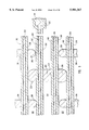
- FIGS. 1A-1F are a sequence of cross-sectional views of a simple non-planar polysilicon structure, illustrating the development of the polysilicon structure, as it progresses through fabrication steps described below.
- FIGS. 2A-2B depicts perspective views that illustrate a principle of the invention described herein by which the effective conductive surface area of the polysilicon structure is increased.
- FIGS. 3A-3I are a sequence of cross-sectional views of a preferred embodiment of the novel transistor structure of the invention described herein, illustrating the development of the novel transistor structure, as it progresses through the fabrication steps described below.
- FIGS. 4A-4C are a sequence of cross sectional views of an alternate embodiment of the novel transistor structure of the invention described herein, illustrating the development thereof as it progresses through the fabrication steps described below.
- FIG. 5 is a top planar view of a DRAM device with a folded bit line architecture having alternating columns of islands, and therein depicting field oxide regions, access transistor gates, storage nodes, active areas, digit nodes, and a contact, wherein the wordlines depicted are formed according to the inventive methods and have both transistor gate structures and parasitic field devices.
- FIGS. 1A-1F represent a fabrication sequence for a simple structure which may be formed using the concepts disclosed in the present invention in which a gate structure is formed upon a substrate assembly.
- substrate assembly is intended herein to mean a substrate having one or more layers or structures formed thereon.
- the substrate assembly may be, by way of example and not by way of limitation, a doped silicon semiconductor substrate typical of a semiconductor wafer.
- a first silicon layer 14 is deposited on top of a base insulation layer 12 on a silicon substrate 10 of a semiconductor wafer.
- Base insulation layer 12 is typically an oxide layer grown directly from a base silicon substrate material on silicon substrate 10, although base insulation layer 12 could also be a deposited oxide layer and the base silicon substrate material on silicon substrate 10 could also be an epitaxial silicon layer or region.
- base insulation layer 12 will have a thickness in a range from about 40 Angstroms to about 150 Angstroms, and preferably from about 90 Angstroms to about 100 Angstroms.
- First silicon layer 14 could be either polysilicon or amorphous silicon and its composition would depend on other device and process factors.
- First silicon layer 14 will typically be deposited by a sputtering or chemical vapor deposition (CVD) process and has a preferred thickness of about 1500 Angstroms.
- First refractory metal layer 16 is then deposited on silicon substrate 10 of the semiconductor wafer on top of first silicon layer 14, First refractory metal layer 16 will typically be titanium silicide although other refractory metal suicides could be used, and will typically be deposited by a CVD process.
- First barrier layer 18 is then deposited on silicon substrate 10 of the semiconductor wafer on top of first refractory metal layer 16.
- First barrier layer 18 will typically be a passivation or insulating material which is readily deposited such as silicon dioxide or silicon nitride, although other materials could be used.
- Second silicon layer 20 is then deposited on silicon substrate 10 of the semiconductor wafer on top of first barrier layer 18.
- Second silicon layer 20 could be either polysilicon or amorphous silicon and its composition would depend on other device and process factors.
- Second silicon layer 20 will typically be deposited by a sputtering or (CVD) process and has a preferred thickness in a range from about 4000 Angstroms to about 5000 Angstroms.
- the semiconductor wafer is then patterned with a photoresist material 22 on top of second silicon layer 20 as shown in FIG. 1B.
- An etch step is then performed to etch second silicon layer 20 leaving silicon riser structures 24 as shown in FIG. 1C.
- Silicon riser structures 24 serve as a mask for first barrier layer 18 during the etch.
- first barrier layer 18 remains only under silicon riser structures 24 as shown in FIG. 1D.
- a second etch is then performed, etching first refractory metal layer 16 and first silicon layer 14. After photoresist material 22 is stripped, there remains complex gate structures 32 which include base polysilicon regions 30 and silicon riser structures 24 as shown in FIG. 1E.
- a second refractory metal layer 36 is then deposited on the semiconductor wafer as shown in FIG. 1F.
- the deposition will typically be either by sputtering or by (CVD) processes.
- CVD achieves better coverage of exposed surfaces which are substantially vertical, such as inner vertical walls of silicon riser structures 24 and is preferred.
- Second refractory metal layer 36 is composed of pure titanium in the preferred a embodiment although other refractory metals such as cobalt, or their stoichiometric suicides, could also be used.
- One or more high temperature annealing steps will then be performed so that the material in first refractory metal layer 24 and second refractory metal layer 36 reacts with the polysilicon material in silicon riser structures 24 and base polysilicon regions 30 to form polycide.
- Material from refractory metal layer 36 that is unreacted with exposed silicon on the semiconductor wafer is then removed using a conventional etching process so that the complex gate structures 32 now appear as shown in FIG. 1F.
- Temperatures during the high temperature annealing steps will be in a range from about 700° C. to about 1100° C. and will vary based on other device fabrication factors. In the preferred embodiment, the temperature chosen is sufficient to transform the titanium silicide formed into the C54 crystalline phase.
- First barrier layer 18 is seen in FIG. 1F as having second refractory metal layer 36 thereon at area 38. Area 38 is covered by second refractory metal layer 36 due to a phenomena know as creep. By way of example of this phenomena, as silicon mixes with the refractory metal with heightened temperature, the reaction product thereof is a refractory metal silicide that tends to grow. Seen in FIG. 1F, second refractory metal layer 36 has grown over area 38 of first barrier layer 18, and thereafter serves as a bridge for second refractory metal layer 36 between first refractory metal layer 16 and silicon riser structure 24. As such, second refractory metal layer 36 serves as a conductive strapping of the illustrated structures seen in FIG. 1F from top to bottom. The strapping arrangement increases the conductive surface area with a low resistivity layer on the resultant structures.
- FIGS. 1A though IF is particularly advantageous for forming a width of base polysilicon region 30 less than 0.25 microns.
- Polysilicon structures such as silicon riser structure 24, can be integrated into fabrication of a Dynamic Random Access (DRAM) device.
- DRAM Dynamic Random Access
- the riser structures contemplated by the present invention can be used in the formation of either a storage node component or a cell plate component of a capacitor structure found in a DRAM device. As such, the riser structure will add surface area to the capacitor so as to realize added charge strength and less time between refresh charging.
- FIGS. 2A-2B are three dimensional cross-section drawings which illustrate the difference in surface areas between a conventional polycide gate structure as shown in FIG. 2A and the complex gate structure which is described herein and is shown in FIG. 2B. It is known in the art that an end-to-end resistance of a rectangular piece of conductive material is directly proportional to the number of squares of the material, said number of squares being a unitless quantity defined as:
- W the width of said conductive material.
- the total width of simple polysilicon structure 40 as shown in FIG. 2A is equal to:
- the total width of complex polysilicon structure 44 is determined by the combination of the surface of simple polysilicon structure 40 and riser polysilicon structure 48 and is equal to:
- FIGS. 3A-3I illustrate an alternative embodiment of the present invention which is adapted to the fabrication of polysilicon MOSFET gate structures and which will now be described.
- a nitride layer 50 is deposited on top of a gate oxide layer 12 of a is silicon substrate 10 of a semiconductor wafer.
- Gate oxide layer 12 is typically an oxide layer grown directly on base silicon substrate material of silicon substrate 10, although gate oxide layer 12 could also be a deposited oxide layer, and the base silicon substrate material of silicon substrate 10 could be an epitaxial silicon layer.
- a nitride layer 50 is typically deposited by a CVD process and in this embodiment is substantially composed of silicon nitride, although other materials could be used.
- a second oxide layer 52 is then deposited on the semiconductor wafer on top of nitride layer 50.
- second oxide layer 52 is typically deposited by a CVD process and is substantially composed of silicon dioxide, although other materials could be used.
- a first silicon layer 54 is then deposited on the semiconductor wafer on top of second oxide layer 52.
- First silicon layer 54 could be either polysilicon or amorphous silicon and its composition would depend on other device and process factors
- First silicon layer 54 is typically deposited by a sputtering or chemical vapor deposition (CVD) process and has a thickness of about 1500 Angstroms.
- the semiconductor wafer is then patterned as shown in FIG. 3B with a photoresist layer 56 and material from nitride layer 50, second oxide layer 52 and first silicon layer 54 is removed, leaving a gate stack 57 as shown in FIG. 3C.
- the etching is performed so that nitride layer 50 is undercut.
- the undercut of nitride layer 50, on each side thereof illustrated in FIG. 3C is preferably about 0.15 microns, leaving the remaining illustrated length of nitride layer 50 preferably about 0.3 microns.
- a second silicon layer 58 is then deposited on the semiconductor wafer as shown in FIG. 3D.
- Second silicon layer 58 will preferably be deposited with a CVD process so that the aforedescribed undercut areas of nitride layer 50 are filled with second silicon layer 58.
- Second silicon layer 58 must also be deposited in such a manner that spacers can be formed on either side of gate stack 57 in a subsequent spacer etch of second silicon layer 58.
- second silicon layer 58 makes conductive contact with the vertical sides of first silicon layer 54, so that a single complex polysilicon gate structure is formed.
- the semiconductor wafer is then patterned and anisotropically etched so that material is removed from first silicon layer 54 leaving silicon gate structures 60 and a gate well 62 as shown in FIG. 3E.
- a second etch which is isotropic, is performed to remove the remaining material of second oxide layer 52 from within gate stack 57.
- the second etch is preferably an oxide etch that is carried out using nitride layer 50 ;s an etch stop. As such, all material in second oxide layer 52 within gate stack 57 is substantially removed, leaving only nitride layer 50.
- a third etch is performed to remove the remaining material of nitride layer 50 from within gate stack 57.
- the third etch is preferably an nitride etch that is carried out using gate oxide layer 12 as an etch stop.
- Refractory metal layer 64 such as titanium is then deposited on the semiconductor wafer as shown in FIG. 3F.
- refractory metal layer 64 is pure titanium and is deposited using chemical vapor deposition (CVD).
- CVD obtains a preferred coverage on the underside of first silicon layer 54 on the inside surface of silicon gate structures 60, thereby increasing the surface area of interfacing between refractory metal layer 64 and silicon surfaces.
- One or more high temperature annealing steps will then be performed so that the material in refractory metal layer 64 reacts with the silicon in silicon gate structures 60 and in source/drain contact regions 66 to form a polycide layer. Temperatures during the high temperature annealing steps will be in a range from about 700° C. to about 1100° C. and will vary based on other device fabrication factors. In this embodiment, titanium will be the material from which refractory metal layer 64 is composed. The temperature will be preferably sufficient to transform the titanium silicide formed from the reaction of refractory metal layer 64 with silicon gate structures 60 and so as to form the C54 crystalline phase upon both silicon gate structures 63.
- Material from refractory metal layer 64 that is unreacted with exposed silicon on the semiconductor wafer is then removed using an conventional etching process leaving a structure as is illustrated in FIG. 3G. Additionally, it may be preferably to remove refractory metal silicide material from surfaces 67 on silicon gate structures 63.
- a first passivation layer 68 is then deposited on the semiconductor wafer as shown in FIG. 3H.
- First passivation layer 68 is typically a material such as BPSG.
- the semiconductor wafer is then patterned with photoresist layer 74 and etched to form a contact plug region 72 as shown in FIG. 3I.
- a titanium/titanium nitride liner 76 is then formed on the inside surfaces of contact plug region 72.
- a tungsten silicide contact plug 78 is then formed within the inside surfaces of titanium/titanium nitride liner 76 within contact plug region 72.
- Seen in 3I is a contact made by titanium/titanium nitride liner 76 with gate oxide layer 12 above source/drain region 66 which is between the two silicon gate structures 60.
- a metal layer 74 is then formed, incident to a metalization process, on top of first passivation layer 68 making conductive contact with the tungsten silicide contact plug.
- FIG. 3I shows that first and second gate tops 61 and first and second gate bottoms 63, in combination, have cross-sectional shapes of a "C” or inverted "C".
- a first silicon layer 54 is formed on top of a gate oxide layer 12 of a silicon substrate 10 of a semiconductor wafer.
- Gate oxide layer 12 is typically an oxide layer grown directly on base silicon substrate material of silicon substrate 10, although gate oxide layer 12 could also be a deposited oxide layer, and the base silicon substrate material of silicon substrate 10 could be an epitaxial silicon layer.
- a nitride layer 50 is formed on top of second oxide layer 54, typically being deposited by a CVD process.
- nitride layer 50 is preferably composed of an electrical insulator such as silica or silicon nitride, although other materials could be used.
- a second silicon layer 55 is then formed on top of nitride layer 50.
- First and second silicon layers 54, 55 could be either polysilicon or amorphous silicon and its composition would depend on other device and process factors.
- First and second silicon layers 54, 55 are typically deposited by a sputtering or chemical vapor deposition (CVD) processes.
- the thickness of first silicon layer 54 is in a range from about 800 Angstroms to about 1500 Angstroms, and is preferably about 1500 Angstroms thick.
- the thickness of second silicon layer 55 is in a range from about 1000 Angstroms to about 2000 Angstroms, and is preferably about 2000 Angstroms thick.
- the semiconductor wafer is then patterned as shown in FIG. 3A with a photoresist layer 56, and then subjected to an etching process.
- the result of the etching process is seen in FIG. 4B, where material from nitride layer 50, and material from first and second silicon layers 54, 55 are removed.
- the etching process is performed so that nitride layer 50 is undercut.
- the undercut of nitride layer 50, on each side thereof illustrated in FIG. 4B is preferably in a range from about 0.05 microns to about 0.1 microns, leaving the remaining illustrated length of nitride layer 50 preferably in a range from about 0.05 microns to about 0.15 microns.
- Refractory metal layer 64 such as titanium is then deposited on the semiconductor wafer as shown in FIG. 4B.
- refractory metal layer 64 is pure titanium and is deposited using chemical vapor deposition (CVD).
- CVD obtains a preferred coverage on the underside of second silicon layer 55, thereby increasing the surface area of interfacing between refractory metal layer 64 and silicon surfaces.
- the undercut regions of nitride layer 50 are also coated the CVD deposited refractory metal layer 64.
- One or more high temperature annealing steps will then be performed so that the material in refractory metal layer 64 reacts with exposed silicon surfaces. Temperatures during the high temperature annealing steps will be in a range from about 550° C. to about 1100° C. and will vary based on other device fabrication factors. In this embodiment, titanium will be the material from which refractory metal layer 64 is composed. The temperature will be preferably sufficient to transform the titanium silicide formed from the reaction of refractory metal layer 64 with silicon surfaces so as to form the C54 crystalline phase upon the silicon surfaces.
- FIG. 4B Material from refractory metal layer 64 that is unreacted with exposed silicon on the semiconductor wafer is then removed using an conventional etching process leaving a structure as is illustrated in FIG. 4B.
- FIG. 4B also shows nitride layer 50 has being coated at the undercut regions thereof by a refractory metal silicide of refractory metal layer 64. Such coating is due to the creep phenomena described above.
- refractory metal layer 64 serves as a conductive strapping between first and second silicon layers 54, 55. The strapping arrangement increases the conductive surface area with a low resistivity layer on the resultant structure.
- a third silicon layer 58 is then deposited on the semiconductor wafer as shown in FIG. 4C.
- Third silicon layer 58 will preferably be deposited with a CVD process so that the aforedescribed undercut areas of nitride layer 50 are filled with third silicon layer 58.
- Third silicon layer 58 must also be deposited in such a manner that spacers can be formed on either side of first and second silicon layers 54, 55 in a subsequent spacer etch of third silicon layer 58.
- third silicon layer 58 makes conductive contact with the vertical sides of first and second silicon layers 54, 55 so that a single complex polysilicon gate structure is formed. Source and drain regions may then be conventionally formed within silicon substrate 10.
- FIG. 4C shows an "I" shape in cross-section from the combination of first and second silicon layers 54, 55 with nitride layer 50.
- FIG. 5 illustrates a top planar view of DRAM structure showing a folded bit line architecture having alternating columns of islands. Seen in FIG. 5 are field oxide regions 202, access transistor gates 204, storage nodes and active areas 206, digit nodes 208, and a contact seen in phantom at 210 at cutaway regions 212.
- the wordlines see in FIG. 5 are formed according to the inventive methods disclosed herein and have both transistor gate structures and parasitic field devices. Each wordline in FIG. 5 is situated on a substrate assembly and is parallel to other wordlines thereon.
- complex gate structure 32 which includes base polysilicon region 30 and silicon riser structure 24 as shown in FIG. 1E can be depicted in top view thereof in FIG. 5.
- each wordline depicted in FIG. 5 can incorporate a structural component having a cross-sectional shape of a "C” or inverted “C” seen in FIG. 3I, or an "I" shape seen in FIG. 4C.
- the structures described above can be integrated into the fabrication of a variety of memory devices, including SRAM, logic memory, flash memory, and DRAM. Such integration can include both wordline gate structures and three dimensional capacitor structures, such as storage node and cell plate capacitor components.
- wordline gate structures can include both wordline gate structures and three dimensional capacitor structures, such as storage node and cell plate capacitor components.
Landscapes
- Engineering & Computer Science (AREA)
- Microelectronics & Electronic Packaging (AREA)
- Power Engineering (AREA)
- General Physics & Mathematics (AREA)
- Computer Hardware Design (AREA)
- Physics & Mathematics (AREA)
- Condensed Matter Physics & Semiconductors (AREA)
- Manufacturing & Machinery (AREA)
- Ceramic Engineering (AREA)
- Chemical & Material Sciences (AREA)
- Chemical Kinetics & Catalysis (AREA)
- Insulated Gate Type Field-Effect Transistor (AREA)
- Electrodes Of Semiconductors (AREA)
Abstract
Description
Wsimple=W
Ssimple=L/W (1)
Wcomplex=W+2*H+(W-2*U)
Wcomplex=2*(W+H-U)
Scomplex=L/(2*(W+H-U)) (2)
Scomplex/Ssimple=W/(2*(W+H+U)) (3)
W=0.25 μ H=0.5 μ U=0.05 μ
Scomplex=0.18*Ssimple
Claims (19)
Priority Applications (5)
| Application Number | Priority Date | Filing Date | Title |
|---|---|---|---|
| US08/733,321 US5981367A (en) | 1996-10-17 | 1996-10-17 | Method for making an access transistor |
| US09/336,885 US6160301A (en) | 1996-10-17 | 1999-06-18 | Gate structure |
| US09/558,887 US6259144B1 (en) | 1996-10-17 | 2000-04-26 | Electronic memory structure |
| US09/629,491 US6365497B1 (en) | 1996-10-17 | 2000-07-31 | Method for making an I - shaped access transistor having a silicide envelop |
| US10/047,633 US6624057B2 (en) | 1996-10-17 | 2002-01-15 | Method for making an access transistor |
Applications Claiming Priority (1)
| Application Number | Priority Date | Filing Date | Title |
|---|---|---|---|
| US08/733,321 US5981367A (en) | 1996-10-17 | 1996-10-17 | Method for making an access transistor |
Related Child Applications (1)
| Application Number | Title | Priority Date | Filing Date |
|---|---|---|---|
| US09/336,885 Division US6160301A (en) | 1996-10-17 | 1999-06-18 | Gate structure |
Publications (1)
| Publication Number | Publication Date |
|---|---|
| US5981367A true US5981367A (en) | 1999-11-09 |
Family
ID=24947133
Family Applications (5)
| Application Number | Title | Priority Date | Filing Date |
|---|---|---|---|
| US08/733,321 Expired - Lifetime US5981367A (en) | 1996-10-17 | 1996-10-17 | Method for making an access transistor |
| US09/336,885 Expired - Fee Related US6160301A (en) | 1996-10-17 | 1999-06-18 | Gate structure |
| US09/558,887 Expired - Lifetime US6259144B1 (en) | 1996-10-17 | 2000-04-26 | Electronic memory structure |
| US09/629,491 Expired - Fee Related US6365497B1 (en) | 1996-10-17 | 2000-07-31 | Method for making an I - shaped access transistor having a silicide envelop |
| US10/047,633 Expired - Fee Related US6624057B2 (en) | 1996-10-17 | 2002-01-15 | Method for making an access transistor |
Family Applications After (4)
| Application Number | Title | Priority Date | Filing Date |
|---|---|---|---|
| US09/336,885 Expired - Fee Related US6160301A (en) | 1996-10-17 | 1999-06-18 | Gate structure |
| US09/558,887 Expired - Lifetime US6259144B1 (en) | 1996-10-17 | 2000-04-26 | Electronic memory structure |
| US09/629,491 Expired - Fee Related US6365497B1 (en) | 1996-10-17 | 2000-07-31 | Method for making an I - shaped access transistor having a silicide envelop |
| US10/047,633 Expired - Fee Related US6624057B2 (en) | 1996-10-17 | 2002-01-15 | Method for making an access transistor |
Country Status (1)
| Country | Link |
|---|---|
| US (5) | US5981367A (en) |
Cited By (11)
| Publication number | Priority date | Publication date | Assignee | Title |
|---|---|---|---|---|
| US6046098A (en) * | 1998-02-23 | 2000-04-04 | Micron Technology, Inc. | Process of forming metal silicide interconnects |
| US6048784A (en) * | 1997-12-17 | 2000-04-11 | Texas Instruments Incorporated | Transistor having an improved salicided gate and method of construction |
| WO2000074126A1 (en) * | 1999-05-27 | 2000-12-07 | Koninklijke Philips Electronics N.V. | A method of manufacturing a semiconductor device |
| US6171981B1 (en) * | 1997-09-11 | 2001-01-09 | Lg Semicon Co., Ltd. | Electrode passivation layer of semiconductor device and method for forming the same |
| US20020190321A1 (en) * | 1998-12-18 | 2002-12-19 | Semiconductor Energy Laboratory Co., Ltd. | Semiconductor device and method of fabricating the same |
| WO2003025981A1 (en) * | 2001-09-19 | 2003-03-27 | Binoptics Corporation | Monolithic three-dimensional structures |
| US20030122132A1 (en) * | 1998-11-25 | 2003-07-03 | Semiconductor Energy Laboratory Co., Ltd. | Semiconductor device, and method of fabricating the same |
| US6798013B2 (en) | 2002-08-28 | 2004-09-28 | Fernando Gonzalez | Vertically integrated flash memory cell and method of fabricating a vertically integrated flash memory cell |
| US20050104068A1 (en) * | 1998-11-17 | 2005-05-19 | Shunpei Yamazaki | Method of fabricating a semiconductor device |
| US20060091387A1 (en) * | 1998-11-25 | 2006-05-04 | Semiconductor Energy Laboratory Co., Ltd. | Semiconductor device |
| US20120161573A1 (en) * | 2010-12-27 | 2012-06-28 | Stmicroelectronics, Inc. | Surface alloy process for mems and nems |
Families Citing this family (11)
| Publication number | Priority date | Publication date | Assignee | Title |
|---|---|---|---|---|
| US5739066A (en) | 1996-09-17 | 1998-04-14 | Micron Technology, Inc. | Semiconductor processing methods of forming a conductive gate and line |
| US6143611A (en) * | 1998-07-30 | 2000-11-07 | Micron Technology, Inc. | Semiconductor processing methods, methods of forming electronic components, and transistors |
| DE10142340B4 (en) * | 2001-08-30 | 2006-04-13 | Infineon Technologies Ag | Field effect transistor with a contact to one of its doping regions and method for its preparation |
| DE10238590B4 (en) * | 2002-08-22 | 2007-02-15 | Infineon Technologies Ag | Method for producing a structure on a substrate |
| JP4526758B2 (en) * | 2002-09-11 | 2010-08-18 | 日鉱金属株式会社 | Iron silicide powder and method for producing the same |
| US6833588B2 (en) * | 2002-10-22 | 2004-12-21 | Advanced Micro Devices, Inc. | Semiconductor device having a U-shaped gate structure |
| US6686637B1 (en) | 2002-11-21 | 2004-02-03 | International Business Machines Corporation | Gate structure with independently tailored vertical doping profile |
| US6753225B1 (en) * | 2003-07-14 | 2004-06-22 | Nanya Technology Corp. | Method of forming a gate structure |
| KR100631943B1 (en) * | 2004-04-22 | 2006-10-04 | 주식회사 하이닉스반도체 | Method for fabricating non-volatile memory device |
| TWI289358B (en) * | 2005-05-27 | 2007-11-01 | Au Optronics Corp | Method for forming low temperature polysilicon thin film transistor within low doped drain structure |
| US8399349B2 (en) | 2006-04-18 | 2013-03-19 | Air Products And Chemicals, Inc. | Materials and methods of forming controlled void |
Citations (5)
| Publication number | Priority date | Publication date | Assignee | Title |
|---|---|---|---|---|
| US5147820A (en) * | 1991-08-26 | 1992-09-15 | At&T Bell Laboratories | Silicide formation on polysilicon |
| US5518958A (en) * | 1994-07-29 | 1996-05-21 | International Business Machines Corporation | Prevention of agglomeration and inversion in a semiconductor polycide process |
| US5576228A (en) * | 1994-11-14 | 1996-11-19 | United Microelectronics Corporation | Method for fabricating polycide gate MOSFET devices |
| US5616948A (en) * | 1995-06-02 | 1997-04-01 | Motorola Inc. | Semiconductor device having electrically coupled transistors with a differential current gain |
| US5698072A (en) * | 1992-06-29 | 1997-12-16 | Sony Corporation | Dry etching method |
Family Cites Families (8)
| Publication number | Priority date | Publication date | Assignee | Title |
|---|---|---|---|---|
| JP2695014B2 (en) * | 1989-09-06 | 1997-12-24 | 株式会社東芝 | MOS type semiconductor device |
| US5395779A (en) * | 1994-04-08 | 1995-03-07 | United Microelectronics Corporation | Process of manufacture of split gate EPROM device |
| KR0141195B1 (en) * | 1994-06-08 | 1998-07-15 | 김광호 | Fabrication method of semiconductor device having low-resistance gate electrod |
| US5543339A (en) * | 1994-08-29 | 1996-08-06 | Motorola, Inc. | Process for forming an electrically programmable read-only memory cell |
| KR100190757B1 (en) * | 1995-06-30 | 1999-06-01 | 김영환 | Method of forming mosfet |
| US6040241A (en) * | 1998-02-11 | 2000-03-21 | United Microelectronics Corp. | Method of avoiding sidewall residue in forming connections |
| US6127251A (en) * | 1998-09-08 | 2000-10-03 | Advanced Micro Devices, Inc. | Semiconductor device with a reduced width gate dielectric and method of making same |
| US6037228A (en) * | 1999-02-12 | 2000-03-14 | United Microelectronics Corp. | Method of fabricating self-aligned contact window which includes forming a undoped polysilicon spacer that extends into a recess of the gate structure |
-
1996
- 1996-10-17 US US08/733,321 patent/US5981367A/en not_active Expired - Lifetime
-
1999
- 1999-06-18 US US09/336,885 patent/US6160301A/en not_active Expired - Fee Related
-
2000
- 2000-04-26 US US09/558,887 patent/US6259144B1/en not_active Expired - Lifetime
- 2000-07-31 US US09/629,491 patent/US6365497B1/en not_active Expired - Fee Related
-
2002
- 2002-01-15 US US10/047,633 patent/US6624057B2/en not_active Expired - Fee Related
Patent Citations (5)
| Publication number | Priority date | Publication date | Assignee | Title |
|---|---|---|---|---|
| US5147820A (en) * | 1991-08-26 | 1992-09-15 | At&T Bell Laboratories | Silicide formation on polysilicon |
| US5698072A (en) * | 1992-06-29 | 1997-12-16 | Sony Corporation | Dry etching method |
| US5518958A (en) * | 1994-07-29 | 1996-05-21 | International Business Machines Corporation | Prevention of agglomeration and inversion in a semiconductor polycide process |
| US5576228A (en) * | 1994-11-14 | 1996-11-19 | United Microelectronics Corporation | Method for fabricating polycide gate MOSFET devices |
| US5616948A (en) * | 1995-06-02 | 1997-04-01 | Motorola Inc. | Semiconductor device having electrically coupled transistors with a differential current gain |
Non-Patent Citations (2)
| Title |
|---|
| W.R. Hunter, et al., New Edge Defined Vertical Etch Approaches for Submircometer Mosfet Fabrication, IEEE, 1980, pp. 764 767. * |
| W.R. Hunter, et al., New Edge-Defined Vertical-Etch Approaches for Submircometer Mosfet Fabrication, IEEE, 1980, pp. 764-767. |
Cited By (37)
| Publication number | Priority date | Publication date | Assignee | Title |
|---|---|---|---|---|
| US6171981B1 (en) * | 1997-09-11 | 2001-01-09 | Lg Semicon Co., Ltd. | Electrode passivation layer of semiconductor device and method for forming the same |
| US6048784A (en) * | 1997-12-17 | 2000-04-11 | Texas Instruments Incorporated | Transistor having an improved salicided gate and method of construction |
| US6281101B1 (en) | 1998-02-23 | 2001-08-28 | Micron Technology, Inc. | Process of forming metal silicide interconnects |
| US6046098A (en) * | 1998-02-23 | 2000-04-04 | Micron Technology, Inc. | Process of forming metal silicide interconnects |
| US20050104068A1 (en) * | 1998-11-17 | 2005-05-19 | Shunpei Yamazaki | Method of fabricating a semiconductor device |
| US9627460B2 (en) | 1998-11-17 | 2017-04-18 | Semiconductor Energy Laboratory Co., Ltd. | Method of fabricating a semiconductor device |
| US8957422B2 (en) | 1998-11-17 | 2015-02-17 | Semiconductor Energy Laboratory Co., Ltd. | Method of fabricating a semiconductor device |
| US8680532B2 (en) | 1998-11-17 | 2014-03-25 | Semiconductor Energy Laboratory Co., Ltd. | Method of fabricating a semiconductor device |
| US8049275B2 (en) | 1998-11-17 | 2011-11-01 | Semiconductor Energy Laboratory Co., Ltd. | Semiconductor device |
| US7439543B2 (en) | 1998-11-17 | 2008-10-21 | Semiconductor Energy Laboratory Co., Ltd. | Semiconductor device comprising thin film transistor comprising conductive film having tapered edge |
| US8373171B2 (en) | 1998-11-25 | 2013-02-12 | Semiconductor Energy Laboratory Co., Ltd. | Light-emitting device having a triple-layer wiring structure |
| US20110233554A1 (en) * | 1998-11-25 | 2011-09-29 | Semiconductor Energy Laboratory Co., Ltd | Semiconductor device, and method of fabricating the same |
| US20030122132A1 (en) * | 1998-11-25 | 2003-07-03 | Semiconductor Energy Laboratory Co., Ltd. | Semiconductor device, and method of fabricating the same |
| US7956362B2 (en) | 1998-11-25 | 2011-06-07 | Semiconductor Energy Laboratory Co., Ltd. | Semiconductor device and wiring structure of triple-layer |
| US9035316B2 (en) | 1998-11-25 | 2015-05-19 | Semiconductor Energy Laboratory Co., Ltd. | Device comprising EL element electrically connected to P-channel transistor |
| US20060091387A1 (en) * | 1998-11-25 | 2006-05-04 | Semiconductor Energy Laboratory Co., Ltd. | Semiconductor device |
| US7064020B2 (en) * | 1998-11-25 | 2006-06-20 | Semiconductor Energy Laboratory Co., Ltd. | Method of manufacturing a semiconductor device having a gate electrode with a three layer structure |
| US7564059B2 (en) | 1998-11-25 | 2009-07-21 | Semiconductor Energy Laboratory Co., Ltd. | Semiconductor device with tapered gates |
| US20060208258A1 (en) * | 1998-11-25 | 2006-09-21 | Semiconductor Energy Laboratory Co., Ltd. | Semiconductor device, and method of fabricating the same |
| US8816347B2 (en) | 1998-12-18 | 2014-08-26 | Semiconductor Energy Laboratory Co., Ltd. | Semiconductor device and method of fabricating the same |
| US20020190321A1 (en) * | 1998-12-18 | 2002-12-19 | Semiconductor Energy Laboratory Co., Ltd. | Semiconductor device and method of fabricating the same |
| US7952093B2 (en) | 1998-12-18 | 2011-05-31 | Semiconductor Energy Laboratory Co., Ltd. | Semiconductor device and method of fabricating the same |
| US9368642B2 (en) | 1998-12-18 | 2016-06-14 | Semiconductor Energy Laboratory Co., Ltd. | Semiconductor device and method of fabricating the same |
| US6891195B2 (en) | 1998-12-18 | 2005-05-10 | Semiconductor Energy Laboratory Co., Ltd. | Semiconductor device and method of fabricating the same |
| US8492768B2 (en) | 1998-12-18 | 2013-07-23 | Semiconductor Energy Laboratory Co., Ltd. | Semiconductor device and method of fabricating the same |
| US8252637B2 (en) | 1998-12-18 | 2012-08-28 | Semiconductor Energy Laboratory Co., Ltd. | Semiconductor device and method of fabricating the same |
| WO2000074126A1 (en) * | 1999-05-27 | 2000-12-07 | Koninklijke Philips Electronics N.V. | A method of manufacturing a semiconductor device |
| WO2003025981A1 (en) * | 2001-09-19 | 2003-03-27 | Binoptics Corporation | Monolithic three-dimensional structures |
| US6653244B2 (en) | 2001-09-19 | 2003-11-25 | Binoptics Corporation | Monolithic three-dimensional structures |
| US20040028327A1 (en) * | 2001-09-19 | 2004-02-12 | Binoptics Corporation | Monolithic three-dimensional structures |
| US7012291B2 (en) | 2001-09-19 | 2006-03-14 | Binoptics Corporation | Monolithic three-dimensional structures |
| US7098122B2 (en) | 2002-08-28 | 2006-08-29 | Micron Technology, Inc. | Method of fabricating a vertically integrated memory cell |
| US20050139950A1 (en) * | 2002-08-28 | 2005-06-30 | Fernando Gonzalez | Vertically integrated flash memory cell and method of fabricating a vertically integrated flash memory cell |
| US6798013B2 (en) | 2002-08-28 | 2004-09-28 | Fernando Gonzalez | Vertically integrated flash memory cell and method of fabricating a vertically integrated flash memory cell |
| US20120161573A1 (en) * | 2010-12-27 | 2012-06-28 | Stmicroelectronics, Inc. | Surface alloy process for mems and nems |
| US9174835B2 (en) * | 2010-12-27 | 2015-11-03 | Stmicroelectronics, Inc. | Microstructure and electronic device |
| US9604845B2 (en) | 2010-12-27 | 2017-03-28 | Stmicroelectronics, Inc. | Methods of forming microstructure and electronic device having moveable component |
Also Published As
| Publication number | Publication date |
|---|---|
| US6365497B1 (en) | 2002-04-02 |
| US6160301A (en) | 2000-12-12 |
| US20020132459A1 (en) | 2002-09-19 |
| US6259144B1 (en) | 2001-07-10 |
| US6624057B2 (en) | 2003-09-23 |
Similar Documents
| Publication | Publication Date | Title |
|---|---|---|
| US5981367A (en) | Method for making an access transistor | |
| US6476488B1 (en) | Method for fabricating borderless and self-aligned polysilicon and metal contact landing plugs for multilevel interconnections | |
| US9076888B2 (en) | Silicided recessed silicon | |
| US6365452B1 (en) | DRAM cell having a vertical transistor and a capacitor formed on the sidewalls of a trench isolation | |
| US5241193A (en) | Semiconductor device having a thin-film transistor and process | |
| KR100295258B1 (en) | Semiconductor integrated circuit device having a capacitor structure with increased capacitance and a method of manufacturing the same | |
| US5408130A (en) | Interconnection structure for conductive layers | |
| US6522001B2 (en) | Local interconnect structures and methods for making the same | |
| US5918118A (en) | Dual deposition methods for forming contact metallizations, capacitors, and memory devices | |
| US5436188A (en) | Dram cell process having elk horn shaped capacitor | |
| US20040036051A1 (en) | Integrated capacitor with enhanced capacitance density and method of fabricating same | |
| KR100360396B1 (en) | Method for forming contact structure of semiconductor device | |
| KR100614290B1 (en) | Method for production of a memory capacitor | |
| US6235627B1 (en) | Semiconductor device and method for manufacturing the same | |
| JP2003519911A (en) | Method of forming semiconductor structure | |
| US6372574B1 (en) | Method of forming a capacitor container electrode and method of patterning a metal layer by selectively silicizing the electrode or metal layer and removing the silicized portion | |
| US6727174B1 (en) | Method for fabricating a dual-diameter electrical conductor | |
| US6184129B1 (en) | Low resistivity poly-silicon gate produced by selective metal growth | |
| US6174762B1 (en) | Salicide device with borderless contact | |
| US7468533B2 (en) | Terraced film stack | |
| US20080020568A1 (en) | Semiconductor device having a silicide layer and method of fabricating the same | |
| TWI262561B (en) | Method of forming ultra-shallow junction devices and its application in a memory device | |
| US6500708B2 (en) | Method for forming capacitor of semiconductor device | |
| EP0836223A2 (en) | Method of forming a silicide layer | |
| KR100277847B1 (en) | Method of manufacturing capacitor of semiconductor device _ |
Legal Events
| Date | Code | Title | Description |
|---|---|---|---|
| AS | Assignment |
Owner name: MICRON TECHNOLOGY, INC., IDAHO Free format text: ASSIGNMENT OF ASSIGNORS INTEREST;ASSIGNOR:GONZALEZ, FERNANDO;REEL/FRAME:008278/0098 Effective date: 19961014 |
|
| STCF | Information on status: patent grant |
Free format text: PATENTED CASE |
|
| FEPP | Fee payment procedure |
Free format text: PAYOR NUMBER ASSIGNED (ORIGINAL EVENT CODE: ASPN); ENTITY STATUS OF PATENT OWNER: LARGE ENTITY |
|
| CC | Certificate of correction | ||
| FPAY | Fee payment |
Year of fee payment: 4 |
|
| FPAY | Fee payment |
Year of fee payment: 8 |
|
| FPAY | Fee payment |
Year of fee payment: 12 |
|
| AS | Assignment |
Owner name: U.S. BANK NATIONAL ASSOCIATION, AS COLLATERAL AGENT, CALIFORNIA Free format text: SECURITY INTEREST;ASSIGNOR:MICRON TECHNOLOGY, INC.;REEL/FRAME:038669/0001 Effective date: 20160426 Owner name: U.S. BANK NATIONAL ASSOCIATION, AS COLLATERAL AGEN Free format text: SECURITY INTEREST;ASSIGNOR:MICRON TECHNOLOGY, INC.;REEL/FRAME:038669/0001 Effective date: 20160426 |
|
| AS | Assignment |
Owner name: MORGAN STANLEY SENIOR FUNDING, INC., AS COLLATERAL AGENT, MARYLAND Free format text: PATENT SECURITY AGREEMENT;ASSIGNOR:MICRON TECHNOLOGY, INC.;REEL/FRAME:038954/0001 Effective date: 20160426 Owner name: MORGAN STANLEY SENIOR FUNDING, INC., AS COLLATERAL Free format text: PATENT SECURITY AGREEMENT;ASSIGNOR:MICRON TECHNOLOGY, INC.;REEL/FRAME:038954/0001 Effective date: 20160426 |
|
| AS | Assignment |
Owner name: U.S. BANK NATIONAL ASSOCIATION, AS COLLATERAL AGENT, CALIFORNIA Free format text: CORRECTIVE ASSIGNMENT TO CORRECT THE REPLACE ERRONEOUSLY FILED PATENT #7358718 WITH THE CORRECT PATENT #7358178 PREVIOUSLY RECORDED ON REEL 038669 FRAME 0001. ASSIGNOR(S) HEREBY CONFIRMS THE SECURITY INTEREST;ASSIGNOR:MICRON TECHNOLOGY, INC.;REEL/FRAME:043079/0001 Effective date: 20160426 Owner name: U.S. BANK NATIONAL ASSOCIATION, AS COLLATERAL AGEN Free format text: CORRECTIVE ASSIGNMENT TO CORRECT THE REPLACE ERRONEOUSLY FILED PATENT #7358718 WITH THE CORRECT PATENT #7358178 PREVIOUSLY RECORDED ON REEL 038669 FRAME 0001. ASSIGNOR(S) HEREBY CONFIRMS THE SECURITY INTEREST;ASSIGNOR:MICRON TECHNOLOGY, INC.;REEL/FRAME:043079/0001 Effective date: 20160426 |
|
| AS | Assignment |
Owner name: MICRON TECHNOLOGY, INC., IDAHO Free format text: RELEASE BY SECURED PARTY;ASSIGNOR:U.S. BANK NATIONAL ASSOCIATION, AS COLLATERAL AGENT;REEL/FRAME:047243/0001 Effective date: 20180629 |
|
| AS | Assignment |
Owner name: MICRON TECHNOLOGY, INC., IDAHO Free format text: RELEASE BY SECURED PARTY;ASSIGNOR:MORGAN STANLEY SENIOR FUNDING, INC., AS COLLATERAL AGENT;REEL/FRAME:050937/0001 Effective date: 20190731 |