EP1110067B1 - Sensor with diaphragm and a plurality of switchable transducers to hit the edge - Google Patents
Sensor with diaphragm and a plurality of switchable transducers to hit the edge Download PDFInfo
- Publication number
- EP1110067B1 EP1110067B1 EP99946594A EP99946594A EP1110067B1 EP 1110067 B1 EP1110067 B1 EP 1110067B1 EP 99946594 A EP99946594 A EP 99946594A EP 99946594 A EP99946594 A EP 99946594A EP 1110067 B1 EP1110067 B1 EP 1110067B1
- Authority
- EP
- European Patent Office
- Prior art keywords
- sensor
- diaphragm
- sensing elements
- etch
- substrate
- Prior art date
- Legal status (The legal status is an assumption and is not a legal conclusion. Google has not performed a legal analysis and makes no representation as to the accuracy of the status listed.)
- Expired - Lifetime
Links
- 239000000758 substrate Substances 0.000 claims description 27
- 229910052710 silicon Inorganic materials 0.000 claims description 8
- 239000010703 silicon Substances 0.000 claims description 8
- 238000000034 method Methods 0.000 description 36
- 235000012431 wafers Nutrition 0.000 description 18
- 238000005530 etching Methods 0.000 description 8
- XUIMIQQOPSSXEZ-UHFFFAOYSA-N Silicon Chemical compound [Si] XUIMIQQOPSSXEZ-UHFFFAOYSA-N 0.000 description 7
- 238000004519 manufacturing process Methods 0.000 description 7
- 238000013459 approach Methods 0.000 description 4
- 238000012545 processing Methods 0.000 description 4
- 239000007858 starting material Substances 0.000 description 4
- 230000003750 conditioning effect Effects 0.000 description 3
- 238000005259 measurement Methods 0.000 description 3
- VYPSYNLAJGMNEJ-UHFFFAOYSA-N Silicium dioxide Chemical compound O=[Si]=O VYPSYNLAJGMNEJ-UHFFFAOYSA-N 0.000 description 2
- 230000008901 benefit Effects 0.000 description 2
- 238000013461 design Methods 0.000 description 2
- 238000009792 diffusion process Methods 0.000 description 2
- 230000035945 sensitivity Effects 0.000 description 2
- 239000000126 substance Substances 0.000 description 2
- 238000012360 testing method Methods 0.000 description 2
- 230000001143 conditioned effect Effects 0.000 description 1
- 239000013078 crystal Substances 0.000 description 1
- 230000001419 dependent effect Effects 0.000 description 1
- 238000007654 immersion Methods 0.000 description 1
- 238000002513 implantation Methods 0.000 description 1
- 239000012212 insulator Substances 0.000 description 1
- 238000005468 ion implantation Methods 0.000 description 1
- 239000000463 material Substances 0.000 description 1
- 238000005498 polishing Methods 0.000 description 1
- 230000000135 prohibitive effect Effects 0.000 description 1
- 239000000523 sample Substances 0.000 description 1
- 239000004065 semiconductor Substances 0.000 description 1
- 235000012239 silicon dioxide Nutrition 0.000 description 1
- 239000000377 silicon dioxide Substances 0.000 description 1
- 238000000427 thin-film deposition Methods 0.000 description 1
Images

Classifications
-
- G—PHYSICS
- G01—MEASURING; TESTING
- G01L—MEASURING FORCE, STRESS, TORQUE, WORK, MECHANICAL POWER, MECHANICAL EFFICIENCY, OR FLUID PRESSURE
- G01L9/00—Measuring steady of quasi-steady pressure of fluid or fluent solid material by electric or magnetic pressure-sensitive elements; Transmitting or indicating the displacement of mechanical pressure-sensitive elements, used to measure the steady or quasi-steady pressure of a fluid or fluent solid material, by electric or magnetic means
- G01L9/0041—Transmitting or indicating the displacement of flexible diaphragms
- G01L9/0051—Transmitting or indicating the displacement of flexible diaphragms using variations in ohmic resistance
- G01L9/0052—Transmitting or indicating the displacement of flexible diaphragms using variations in ohmic resistance of piezoresistive elements
- G01L9/0055—Transmitting or indicating the displacement of flexible diaphragms using variations in ohmic resistance of piezoresistive elements bonded on a diaphragm
-
- G—PHYSICS
- G01—MEASURING; TESTING
- G01L—MEASURING FORCE, STRESS, TORQUE, WORK, MECHANICAL POWER, MECHANICAL EFFICIENCY, OR FLUID PRESSURE
- G01L9/00—Measuring steady of quasi-steady pressure of fluid or fluent solid material by electric or magnetic pressure-sensitive elements; Transmitting or indicating the displacement of mechanical pressure-sensitive elements, used to measure the steady or quasi-steady pressure of a fluid or fluent solid material, by electric or magnetic means
- G01L9/02—Measuring steady of quasi-steady pressure of fluid or fluent solid material by electric or magnetic pressure-sensitive elements; Transmitting or indicating the displacement of mechanical pressure-sensitive elements, used to measure the steady or quasi-steady pressure of a fluid or fluent solid material, by electric or magnetic means by making use of variations in ohmic resistance, e.g. of potentiometers, electric circuits therefor, e.g. bridges, amplifiers or signal conditioning
- G01L9/06—Measuring steady of quasi-steady pressure of fluid or fluent solid material by electric or magnetic pressure-sensitive elements; Transmitting or indicating the displacement of mechanical pressure-sensitive elements, used to measure the steady or quasi-steady pressure of a fluid or fluent solid material, by electric or magnetic means by making use of variations in ohmic resistance, e.g. of potentiometers, electric circuits therefor, e.g. bridges, amplifiers or signal conditioning of piezo-resistive devices
Definitions
- the present invention relates to a (pressure) sensor. More particularly, the present invention is directed to providing a monolithic sensor having multiple sensing elements on a single substrate and electrically selecting one of the sensing elements.
- Etching a sensor diaphragm to a desired thickness allows the diaphragm to deflect properly upon exposure to the source of pressure to be sensed.
- the deflection of the diaphragm is dependent on the pressure being exerted and the thickness and size of the diaphragm. Therefore, in order to have sensors that produce a consistent response from sensor-to-sensor, the prior art diaphragm thickness must be maintained within relatively strict tolerances.
- the prior art typically used one of several well known processes to etch the diaphragm, including timed-cavity-etch, oxide etch-stop, and electrochemical etch-stop.
- the timed-cavity-etch process is performed by repeatedly interrupting the etching for thickness measurements and resuming etching until a specified diaphragm thickness is achieved. If a cavity is over-etched or under-etched, then the diaphragm is not the desired thickness to provide the proper structural response of the diaphragm and therefore must be discarded. Due to the constant stopping, measuring, and resuming, the process introduces many opportunities for the substrate to break, increasing the possibility of low-manufacturing yields. In addition, the timed-etch process typically requires greater labor and more time than other etch techniques that employ an etch-stop layer.
- the oxide etch-stop process uses a starting material for the sensor substrate that consists of two silicon wafers bonded together, with a silicon dioxide layer in between. (The internal oxide layer is created by growing it on one of the wafers before they are bonded together.) When the cavity is etched by immersion in a chemical bath which is exposed to one surface of the bonded wafer/substrate, silicon is removed until it reaches the oxide layer which resists removal by the etchant.
- the diaphragm thickness is defined by precisely polishing the other surface of the wafer substrate to the desired thickness.
- the oxide etch stop process is simpler than timed etch, but is offset by the high cost of the bonded and polished starting material wafers used as the sensor substrate. The availability of bonded/SOI wafers is typically limited. Also, the diaphragm thickness must be pre-determined and therefore the flexibility to change pressure ranges if product mix changes is severely limited.
- the electrochemical etch-stop process also provides a precise diaphragm thickness.
- the starting material used as the sensor substrate consists of a silicon wafer which has undergone a wafer processing step to add a P-type (in an N-substrate) or N-type layer (in a P-substrate) by means of diffusion, ion implantation, or epitaxial growth or other known process.
- the wafer is etched in a fixture which applies bias to the N and P regions such that an etch stop layer is created when the chemical etchant reaches the layer which was deposited to define the desired diaphragm thickness (e.g. N epitaxial layer deposited on P substrate).
- the diaphragm thickness must be pre-determined and sets the pressure range of the sensor well ahead of the etch process.
- a different diaphragm thickness requires a wafer with an N or P layer added at a different level in the wafer.
- the extra processing to create the etch stop layer adds cost to the wafer starting material compared to the bulk silicon wafers used in the timed etch process.
- etch process fixturing to electrically make contact with the wafer and properly bias it to create an etch stop at the PN junction complicates the manufacturing process, and presents the potential for electrical leakage which could inhibit or damage the etch process.
- bridge The most common (so-called "bridge” approach) involves placing four piezoresistors, one on each edge of the square or rectangular diaphragm.
- the piezoresistors are connected together in a wheatstone bridge configuration to sense one specific pressure range.
- the other approach locates a single piezoresistive element at one edge of the diaphragm.
- the piezoresistive element is oriented relative to the silicon crystal structure to provide maximum sensitivity of the sensor output when it is accurately placed at the maximum stress point near the diaphragm edge.
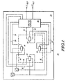
- FIG. 1 shows a sensor 10, in accordance with the present invention.
- Sensor 10 includes a sensor substrate 12, sensing elements 14, 16, 18, and 20, and electronic switching circuit 22.
- the sensing elements 14-20 are preferably formed by implantation, diffusion, thin-film deposition, or other well known techniques.
- Switching circuit 22 is electrically connected to each of the sensing elements 14-20 via lines 28, 30, 32, 34, 36, 38, 40, and 42 for electrically selecting at least one of the sensing elements 14-20.
- Lines 28, 32, 36, and 42 preferably carry a S + (positive sensor output) signal and lines 30, 34, 38, and 40 preferably carry a S - (negative sensor output) signal.
- Switching circuit 22 is preferably formed on substrate 12 by a standard semiconductor fabrication process or other well known techniques.
- switching circuit 22 selects the desired sensor element for measurement by electrically (digitally) connecting the S + and S - terminals of the sensor to a signal conditioning circuit which measures the differential output voltage of each defined sensing element 14-20 and amplifies and compensates the desired sensing element output signals for use by an external system.
- power V + and V -
- sensing elements 14-20 are selected by connecting the desired output signal terminals S + and S - .
- Other switching configurations can also be used. For example, all S + , S - , and V + leads could be connected to circuit 22 and then switching in the appropriate V - connection for the desired element (see Fig. 8 below). Other alternative embodiments are described in detail below.
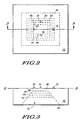
- Sensing elements 14-20 are disposed at varying distances from an outer edge 44 of a cavity 51. It is well known that sensors provide the best performance when the sensing elements are placed adjacent an edge of the diaphragm 46. Also, sensor sensitivity is a function of diaphragm thickness and size. By placing the elements 14-20 at varying distances from the edge 44 of the cavity opening an inexpensive timed etch method can be used. In this way, the edge of the diaphragm 46 can be formed essentially at one of the edges 43, 45, 47, and 49 as indicated in FIGs. 2 and 3. Therefore, during the timed etch process, a repeated etch and measurement cycle to measure diaphragm thickness and stop etching at a precise nominal diaphragm thickness can be minimized.
- the etching process timing window is widened by virtue of a wider range of diaphragm thicknesses that still produce usable sensors 10.
- the possibility of over-etch or under-etch is reduced because of an increase in the target diaphragm thickness window.
- FIGs. 2 and 3 show four possible diaphragm 46 thicknesses with corresponding diaphragm edges 43, 45, 47, and 49 defining the optimal edges of diaphragm 46 for each of the sensing elements 14-20. It is noted that each of the sensing elements 14-20 are preferably positioned on substrate 12 directly above one of the edges 43-49 for optimum performance.
- the on-chip switching circuit 22 is needed to select the element 14-20 that provides performance closest to the nominal target.
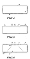
- FIGs. 4, 5, and 6 are cross-sectional views of various stages of a preferred method of manufacture of the sensor 10.
- FIG. 4 shows the first step of the method where a sensing substrate 12 is provided and preferably made of silicon or other suitable material.
- Substrate 12 has a top surface 50 opposed to a bottom surface 52.
- FIG. 5 shows the next step of deposing sensing elements 14-20 and electronic switching circuit 22 on the top surface 50. It is noted that electrical interconnect lines 28-42 are also formed at this time but are not shown.
- FIG. 6 shows the final step of removing a portion of substrate 12 from the bottom surface 52 through an etching process to form a cavity 51 to form a diaphragm 46. It is noted that a timed-etch process is preferred but any etching process could be employed depending on the precision required in the placement of the elements 14-20 and the thickness of the diaphragm 46.
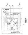
- FIG. 7 discloses an alternate embodiment in accordance with the present invention.
- Electronic switching circuit 24 selects the desired sensing elements 114-120.
- the circuit 24 is preferably on-chip (monolithic), but may be off-chip as well.
- Sensor 55 is similar to sensor 10 described above except that sensor 55 has electronic switching circuit 24 instead of circuit 22.
- Circuit 24 deposed on substrate 57 has a switched electrical connection with the sensing elements via lines 54, 56, 58, and 60 as shown for electronically powering at least one of the sensing elements.
- one of lines 54, 56, 58, and 60 connects the sensor V - terminal (ground terminal) to the power supply by selecting an appropriate digital code that is implemented by the switching circuit 24.
- FIG. 8 discloses yet another preferred embodiment in accordance with the present invention.
- the sensor 66 includes a substrate 68, having a diaphragm 70 defined by edge 72, sensing elements 74, 76, 78 and 80, and a switching circuit defined by box 82.
- Switching circuit 82 includes 12 switches 84, which are preferably FETS as shown. The switches 84 are connected to one of the four input terminals 86, 88, 90, and 92.
- input terminals 86-92 are connected to a microprocessor (not shown) or other logic circuitry and select the sensing element to be used. For example, if sensing element 74 is to be used, a signal would be sent through terminal 86 causing the three transistors 84 associated with the element 74 to turn on causing a signal to be outputted to terminals 94 and 96 from element 74. As can be seen, each of the elements 74-80 is always connected to the high-side voltage terminal 98. Switching the low-side power supply voltage terminal and the two output signal terminals of each element 74-80 ensures a clean signal is supplied to terminals 94 and 96. As disclosed above, the sensor can select an element by switching only the power or switching the output terminals. However, by switching both a power terminal and the output terminals, a cleaner signal at terminals 94 & 96 is caused.
- the technique described above selects elements to accommodate process variations in cavity etch and diaphragm edge location.
- the sensors can also be used to make multiple pressure sensor range die. Instead of placing sensing elements on a substrate to cover a wider range of etch conditions for a single targeted pressure range, sensing elements can be placed so that they are optimized for different pressure ranges. Each sensing element has its own target diaphragm size (cavity edge) and thickness. This may be done in conjunction with the same or different size cavity. Generally, the thicker the diaphragm 46 the higher the pressure range that will be sensed by sensor 10.
- a sensor 10 having a diaphragm edge corresponding with line 43 and having a thicker diaphragm will be used for a higher pressure range than a sensor 10 having a diaphragm edge corresponding to any of lines 45-49 and having a thinner diaphragm.
- An advantage of this invention is that only one integrated sensor design, mask set, and fabrication process is needed for the top side of the substrate. The top side of the substrate is where the complicated and costly signal conditioning and wafer processing is done. By only modifying the etch time and/or the backside cavity opening (this is only one low cost mask), four different pressure range sensors can be manufactured from the same integrated circuit wafers.
Landscapes
- Physics & Mathematics (AREA)
- General Physics & Mathematics (AREA)
- Measuring Fluid Pressure (AREA)
- Pressure Sensors (AREA)
- Semiconductor Integrated Circuits (AREA)
Applications Claiming Priority (3)
| Application Number | Priority Date | Filing Date | Title |
|---|---|---|---|
| US137765 | 1998-08-21 | ||
| US09/137,765 US6142021A (en) | 1998-08-21 | 1998-08-21 | Selectable pressure sensor |
| PCT/US1999/018474 WO2000011441A2 (en) | 1998-08-21 | 1999-08-12 | Pressure sensor and method of forming the same |
Publications (3)
| Publication Number | Publication Date |
|---|---|
| EP1110067A2 EP1110067A2 (en) | 2001-06-27 |
| EP1110067A4 EP1110067A4 (en) | 2001-10-24 |
| EP1110067B1 true EP1110067B1 (en) | 2004-03-17 |
Family
ID=22478952
Family Applications (1)
| Application Number | Title | Priority Date | Filing Date |
|---|---|---|---|
| EP99946594A Expired - Lifetime EP1110067B1 (en) | 1998-08-21 | 1999-08-12 | Sensor with diaphragm and a plurality of switchable transducers to hit the edge |
Country Status (6)
| Country | Link |
|---|---|
| US (1) | US6142021A (enExample) |
| EP (1) | EP1110067B1 (enExample) |
| JP (1) | JP2002523736A (enExample) |
| DE (1) | DE69915651T2 (enExample) |
| ES (1) | ES2217809T3 (enExample) |
| WO (1) | WO2000011441A2 (enExample) |
Families Citing this family (4)
| Publication number | Priority date | Publication date | Assignee | Title |
|---|---|---|---|---|
| US6790699B2 (en) | 2002-07-10 | 2004-09-14 | Robert Bosch Gmbh | Method for manufacturing a semiconductor device |
| DE102007062711A1 (de) * | 2007-12-27 | 2009-07-02 | Robert Bosch Gmbh | Halbleiterwafer mit einer Vielzahl von Sensorelementen und Verfahren zum Vermessen von Sensorelementen auf einem Halbleiterwafer |
| US7926353B2 (en) * | 2009-01-16 | 2011-04-19 | Infineon Technologies Ag | Pressure sensor including switchable sensor elements |
| GB2515715A (en) | 2012-11-21 | 2015-01-07 | Continental Automotive Systems | Piezoresistive transducer with low thermal noise |
Family Cites Families (16)
| Publication number | Priority date | Publication date | Assignee | Title |
|---|---|---|---|---|
| US3456226A (en) * | 1967-10-27 | 1969-07-15 | Conrac Corp | Strain gage configuration |
| JPS5217780A (en) * | 1975-07-04 | 1977-02-09 | Hitachi Ltd | Pressure convertor with semi-conductor elements |
| US4322980A (en) * | 1979-11-08 | 1982-04-06 | Hitachi, Ltd. | Semiconductor pressure sensor having plural pressure sensitive diaphragms and method |
| US4400681A (en) * | 1981-02-23 | 1983-08-23 | General Motors Corporation | Semiconductor pressure sensor with slanted resistors |
| CA1186163A (en) * | 1982-01-04 | 1985-04-30 | James B. Starr | Semiconductor pressure transducer |
| US4539554A (en) * | 1982-10-18 | 1985-09-03 | At&T Bell Laboratories | Analog integrated circuit pressure sensor |
| JPS6077470A (ja) * | 1983-10-04 | 1985-05-02 | Nec Corp | ダイアフラム型半導体圧力センサ |
| US4996082A (en) * | 1985-04-26 | 1991-02-26 | Wisconsin Alumni Research Foundation | Sealed cavity semiconductor pressure transducers and method of producing the same |
| US4885621A (en) * | 1988-05-02 | 1989-12-05 | Delco Electronics Corporation | Monolithic pressure sensitive integrated circuit |
| US5058435A (en) * | 1989-06-22 | 1991-10-22 | Ic Sensors, Inc. | Single diaphragm transducer with multiple sensing elements |
| US5220838A (en) * | 1991-03-28 | 1993-06-22 | The Foxboro Company | Overpressure-protected, differential pressure sensor and method of making the same |
| US5264075A (en) * | 1992-11-06 | 1993-11-23 | Ford Motor Company | Fabrication methods for silicon/glass capacitive absolute pressure sensors |
| US5427975A (en) * | 1993-05-10 | 1995-06-27 | Delco Electronics Corporation | Method of micromachining an integrated sensor on the surface of a silicon wafer |
| WO1995002164A1 (en) * | 1993-07-07 | 1995-01-19 | Ic Sensors, Inc. | Pulsed thermal flow sensor system |
| DE19527687A1 (de) * | 1995-07-28 | 1997-01-30 | Bosch Gmbh Robert | Sensor |
| US5672808A (en) * | 1996-06-11 | 1997-09-30 | Moore Products Co. | Transducer having redundant pressure sensors |
-
1998
- 1998-08-21 US US09/137,765 patent/US6142021A/en not_active Expired - Lifetime
-
1999
- 1999-08-12 EP EP99946594A patent/EP1110067B1/en not_active Expired - Lifetime
- 1999-08-12 JP JP2000566649A patent/JP2002523736A/ja active Pending
- 1999-08-12 ES ES99946594T patent/ES2217809T3/es not_active Expired - Lifetime
- 1999-08-12 DE DE69915651T patent/DE69915651T2/de not_active Expired - Lifetime
- 1999-08-12 WO PCT/US1999/018474 patent/WO2000011441A2/en not_active Ceased
Also Published As
| Publication number | Publication date |
|---|---|
| EP1110067A4 (en) | 2001-10-24 |
| EP1110067A2 (en) | 2001-06-27 |
| DE69915651D1 (de) | 2004-04-22 |
| JP2002523736A (ja) | 2002-07-30 |
| DE69915651T2 (de) | 2004-08-19 |
| ES2217809T3 (es) | 2004-11-01 |
| US6142021A (en) | 2000-11-07 |
| WO2000011441A3 (en) | 2000-06-02 |
| WO2000011441A2 (en) | 2000-03-02 |
Similar Documents
| Publication | Publication Date | Title |
|---|---|---|
| US7493822B2 (en) | Small gauge pressure sensor using wafer bonding and electrochemical etch stopping | |
| US6912759B2 (en) | Method of manufacturing a thin piezo resistive pressure sensor | |
| US4766666A (en) | Semiconductor pressure sensor and method of manufacturing the same | |
| US5155061A (en) | Method for fabricating a silicon pressure sensor incorporating silicon-on-insulator structures | |
| EP1845353B1 (en) | Quartz sensor system | |
| US4771638A (en) | Semiconductor pressure sensor | |
| US7165455B2 (en) | Surface acoustic wave sensor methods and systems | |
| US7997142B2 (en) | Low pressure sensor device with high accuracy and high sensitivity | |
| US8381596B2 (en) | CMOS compatible pressure sensor for low pressures | |
| CN101458134A (zh) | 半导体压力传感器及其制造方法、半导体装置和电子设备 | |
| US6725725B1 (en) | Micromechanical differential pressure sensor device | |
| JPH06307960A (ja) | 圧力センサ | |
| US20050132813A1 (en) | Sealed diaphragm pressure sensor | |
| USRE34893E (en) | Semiconductor pressure sensor and method of manufacturing same | |
| US8647908B2 (en) | Semiconductor pressure sensor and method of manufacturing semiconductor pressure sensor | |
| US20020149069A1 (en) | Piezoresistive sensor with epi-pocket isolation | |
| EP1110067B1 (en) | Sensor with diaphragm and a plurality of switchable transducers to hit the edge | |
| KR100904994B1 (ko) | 압력센서 제조방법 및 그 구조 | |
| US4881056A (en) | Facedown-type semiconductor pressure sensor with spacer | |
| US5747691A (en) | Angular velocity sensor apparatus | |
| JPH10300605A (ja) | 半導体圧力センサ及びセンサチップの製造方法 | |
| US9790082B1 (en) | CMOS and pressure sensor integrated on a chip and fabrication method | |
| JP2519393B2 (ja) | 半導体力学量センサの製造方法 | |
| JP2794147B2 (ja) | 圧力センサ | |
| JPH04323566A (ja) | 半導体加速度センサ |
Legal Events
| Date | Code | Title | Description |
|---|---|---|---|
| PUAI | Public reference made under article 153(3) epc to a published international application that has entered the european phase |
Free format text: ORIGINAL CODE: 0009012 |
|
| 17P | Request for examination filed |
Effective date: 20010321 |
|
| AK | Designated contracting states |
Kind code of ref document: A2 Designated state(s): AT BE CH CY DE DK ES FI FR GB GR IE IT LI LU MC NL PT SE |
|
| A4 | Supplementary search report drawn up and despatched |
Effective date: 20010906 |
|
| AK | Designated contracting states |
Kind code of ref document: A4 Designated state(s): AT BE CH CY DE DK ES FI FR GB GR IE IT LI LU MC NL PT SE |
|
| 17Q | First examination report despatched |
Effective date: 20030326 |
|
| GRAP | Despatch of communication of intention to grant a patent |
Free format text: ORIGINAL CODE: EPIDOSNIGR1 |
|
| RIC1 | Information provided on ipc code assigned before grant |
Ipc: 7G 01L 27/00 B Ipc: 7G 01L 9/06 B Ipc: 7G 01L 1/00 B Ipc: 7G 01D 18/00 A |
|
| RTI1 | Title (correction) |
Free format text: SENSOR WITH DIAPHRAGM AND A PLURALITY OF SWITCHABLE TRANSDUCERS TO HIT THE EDGE |
|
| RIC1 | Information provided on ipc code assigned before grant |
Ipc: 7G 01L 27/00 B Ipc: 7G 01L 9/06 B Ipc: 7G 01L 1/00 B Ipc: 7G 01D 18/00 A |
|
| RTI1 | Title (correction) |
Free format text: SENSOR WITH DIAPHRAGM AND A PLURALITY OF SWITCHABLE TRANSDUCERS TO HIT THE EDGE |
|
| GRAS | Grant fee paid |
Free format text: ORIGINAL CODE: EPIDOSNIGR3 |
|
| GRAA | (expected) grant |
Free format text: ORIGINAL CODE: 0009210 |
|
| AK | Designated contracting states |
Kind code of ref document: B1 Designated state(s): DE ES FR GB IT |
|
| REG | Reference to a national code |
Ref country code: GB Ref legal event code: FG4D |
|
| REG | Reference to a national code |
Ref country code: IE Ref legal event code: FG4D |
|
| REF | Corresponds to: |
Ref document number: 69915651 Country of ref document: DE Date of ref document: 20040422 Kind code of ref document: P |
|
| REG | Reference to a national code |
Ref country code: ES Ref legal event code: FG2A Ref document number: 2217809 Country of ref document: ES Kind code of ref document: T3 |
|
| ET | Fr: translation filed | ||
| PLBE | No opposition filed within time limit |
Free format text: ORIGINAL CODE: 0009261 |
|
| STAA | Information on the status of an ep patent application or granted ep patent |
Free format text: STATUS: NO OPPOSITION FILED WITHIN TIME LIMIT |
|
| 26N | No opposition filed |
Effective date: 20041220 |
|
| REG | Reference to a national code |
Ref country code: IE Ref legal event code: MM4A |
|
| PGFP | Annual fee paid to national office [announced via postgrant information from national office to epo] |
Ref country code: IT Payment date: 20080816 Year of fee payment: 10 |
|
| PGFP | Annual fee paid to national office [announced via postgrant information from national office to epo] |
Ref country code: ES Payment date: 20090805 Year of fee payment: 11 |
|
| PG25 | Lapsed in a contracting state [announced via postgrant information from national office to epo] |
Ref country code: IT Free format text: LAPSE BECAUSE OF NON-PAYMENT OF DUE FEES Effective date: 20090812 |
|
| REG | Reference to a national code |
Ref country code: ES Ref legal event code: FD2A Effective date: 20111019 |
|
| PG25 | Lapsed in a contracting state [announced via postgrant information from national office to epo] |
Ref country code: ES Free format text: LAPSE BECAUSE OF NON-PAYMENT OF DUE FEES Effective date: 20100813 |
|
| REG | Reference to a national code |
Ref country code: FR Ref legal event code: PLFP Year of fee payment: 18 |
|
| PGFP | Annual fee paid to national office [announced via postgrant information from national office to epo] |
Ref country code: DE Payment date: 20160831 Year of fee payment: 18 Ref country code: GB Payment date: 20160819 Year of fee payment: 18 |
|
| PGFP | Annual fee paid to national office [announced via postgrant information from national office to epo] |
Ref country code: FR Payment date: 20160822 Year of fee payment: 18 |
|
| REG | Reference to a national code |
Ref country code: DE Ref legal event code: R119 Ref document number: 69915651 Country of ref document: DE |
|
| GBPC | Gb: european patent ceased through non-payment of renewal fee |
Effective date: 20170812 |
|
| REG | Reference to a national code |
Ref country code: FR Ref legal event code: ST Effective date: 20180430 |
|
| PG25 | Lapsed in a contracting state [announced via postgrant information from national office to epo] |
Ref country code: DE Free format text: LAPSE BECAUSE OF NON-PAYMENT OF DUE FEES Effective date: 20180301 Ref country code: GB Free format text: LAPSE BECAUSE OF NON-PAYMENT OF DUE FEES Effective date: 20170812 |
|
| PG25 | Lapsed in a contracting state [announced via postgrant information from national office to epo] |
Ref country code: FR Free format text: LAPSE BECAUSE OF NON-PAYMENT OF DUE FEES Effective date: 20170831 |