EP1108203B1 - Vor umwelteinflüssen geschütztes mikromechanisches bauelement - Google Patents
Vor umwelteinflüssen geschütztes mikromechanisches bauelement Download PDFInfo
- Publication number
- EP1108203B1 EP1108203B1 EP99953629A EP99953629A EP1108203B1 EP 1108203 B1 EP1108203 B1 EP 1108203B1 EP 99953629 A EP99953629 A EP 99953629A EP 99953629 A EP99953629 A EP 99953629A EP 1108203 B1 EP1108203 B1 EP 1108203B1
- Authority
- EP
- European Patent Office
- Prior art keywords
- wafer
- component
- membrane
- micromechanical
- coating
- Prior art date
- Legal status (The legal status is an assumption and is not a legal conclusion. Google has not performed a legal analysis and makes no representation as to the accuracy of the status listed.)
- Expired - Lifetime
Links
Images
Classifications
-
- G—PHYSICS
- G01—MEASURING; TESTING
- G01L—MEASURING FORCE, STRESS, TORQUE, WORK, MECHANICAL POWER, MECHANICAL EFFICIENCY, OR FLUID PRESSURE
- G01L9/00—Measuring steady of quasi-steady pressure of fluid or fluent solid material by electric or magnetic pressure-sensitive elements; Transmitting or indicating the displacement of mechanical pressure-sensitive elements, used to measure the steady or quasi-steady pressure of a fluid or fluent solid material, by electric or magnetic means
- G01L9/0041—Transmitting or indicating the displacement of flexible diaphragms
- G01L9/0042—Constructional details associated with semiconductive diaphragm sensors, e.g. etching, or constructional details of non-semiconductive diaphragms
-
- B—PERFORMING OPERATIONS; TRANSPORTING
- B81—MICROSTRUCTURAL TECHNOLOGY
- B81C—PROCESSES OR APPARATUS SPECIALLY ADAPTED FOR THE MANUFACTURE OR TREATMENT OF MICROSTRUCTURAL DEVICES OR SYSTEMS
- B81C1/00—Manufacture or treatment of devices or systems in or on a substrate
- B81C1/00865—Multistep processes for the separation of wafers into individual elements
- B81C1/00896—Temporary protection during separation into individual elements
-
- B—PERFORMING OPERATIONS; TRANSPORTING
- B81—MICROSTRUCTURAL TECHNOLOGY
- B81B—MICROSTRUCTURAL DEVICES OR SYSTEMS, e.g. MICROMECHANICAL DEVICES
- B81B2201/00—Specific applications of microelectromechanical systems
- B81B2201/02—Sensors
- B81B2201/0228—Inertial sensors
- B81B2201/0235—Accelerometers
-
- B—PERFORMING OPERATIONS; TRANSPORTING
- B81—MICROSTRUCTURAL TECHNOLOGY
- B81B—MICROSTRUCTURAL DEVICES OR SYSTEMS, e.g. MICROMECHANICAL DEVICES
- B81B2201/00—Specific applications of microelectromechanical systems
- B81B2201/02—Sensors
- B81B2201/0257—Microphones or microspeakers
-
- B—PERFORMING OPERATIONS; TRANSPORTING
- B81—MICROSTRUCTURAL TECHNOLOGY
- B81B—MICROSTRUCTURAL DEVICES OR SYSTEMS, e.g. MICROMECHANICAL DEVICES
- B81B2201/00—Specific applications of microelectromechanical systems
- B81B2201/02—Sensors
- B81B2201/0264—Pressure sensors
-
- B—PERFORMING OPERATIONS; TRANSPORTING
- B81—MICROSTRUCTURAL TECHNOLOGY
- B81C—PROCESSES OR APPARATUS SPECIALLY ADAPTED FOR THE MANUFACTURE OR TREATMENT OF MICROSTRUCTURAL DEVICES OR SYSTEMS
- B81C2201/00—Manufacture or treatment of microstructural devices or systems
- B81C2201/05—Temporary protection of devices or parts of the devices during manufacturing
- B81C2201/053—Depositing a protective layers
Definitions
- the invention relates to a micromechanical component, preferably a micromechanical sensor comprising a wafer, a membrane, a cavity, one or more as a support for the membrane serving sacrificial layers, auxiliary layers, optionally an integrated into the device electronics and at least one opening which connects the membrane produces the environment of the device.
- a micromechanical component preferably a micromechanical sensor comprising a wafer, a membrane, a cavity, one or more as a support for the membrane serving sacrificial layers, auxiliary layers, optionally an integrated into the device electronics and at least one opening which connects the membrane produces the environment of the device.
- Micromechanical devices are in a series of documents described.
- document US-A-5,335,550 discloses a pressure sensor consisting of two semiconductor substrates composed. It is in one of the semiconductor substrates a recess provided later as a cavity or vacuum chamber for the pressure sensor. Furthermore are on the Surface of the second semiconductor substrate by diffusion generated resistors and a corresponding wiring provided.
- the two semiconductor substrates are insulated Film interconnected, so that below the by diffusion generated resistors on the back of the second semiconductor substrate of the cavity is formed.
- Document BP-A 0 624 900 discloses such a method of manufacture of integrated sensors. For this purpose, starting from a substrate surface trenches generated in the substrate, the then used to generate the actual cavity become.
- Micromechanical components for example for use as microphone sensors, pressure sensors or acceleration sensors, are known for example from EP-A 0 714 017.
- the described micromechanical components have a Cavity on, on one side of one example bounded membrane made of metal or polysilicon is.
- the membrane layer is in one area electrically made conductive and forms together with one the opposite side of the cavity arranged counter electrode an electrical capacitance which is used for the measurement used by temporal volume changes of the cavity becomes.
- above the Membrane surface further layers can be arranged, which is a To cause stiffening of the membrane.
- additional Layers are used to improve the mobility of the membrane etched on top of the membrane surface down reaching openings. These openings may be of any shape, e.g. round or be angular. It is also possible that the openings channels are, which are closed in a ring, for example in the form of a square or a circle.
- the possibly large number of above the membrane layer arranged layers and in particular due to the Layers in contact with the environment in a micromechanical device of the above Type require additional measures to protect against external Environmental factors, such as humidity, etc., which affect the environment the function of the micromechanical loading element can result.
- the device for example during a pressure measurement with an aggressive medium in Contact, so the sensitive layers are predominantly in Area of contact points of different layers chemically or physically attacked.
- the components have been so far after separation encapsulated into chips or wrapped in other ways, For example, with a rubber or by coating the Device with a gel in a suitable housing.
- an object of the present Invention provides a method of manufacture a micromechanical device, preferably a micromechanical sensor in conventional semiconductor technology, which protects against environmental influences Micromechanical device preferably a sensor for Provides and without additional protection measures of the device after the separation of the wafer into chips gets along.
- Another object of the invention is to provide a Micromechanical device, preferably a micromechanical Sensors, which are not retroactive, for example externally protected or encapsulated after separation into chips must become.
- a method for producing a micromechanical component preferably a micromechanical sensor comprising the production a micromechanical device made of a wafer 1, a membrane 2, a cavity 3, one or more than Pad for the diaphragm serving sacrificial layers 4, which are arranged on the wafer, auxiliary layers 7 for planarization the component surface and / or for receiving Conductor tracks or semiconductor devices, at least one Opening 6, which connects the environment of the device produces the membrane and possibly one or more Circuit protection layers on the auxiliary layers 7, which characterized in that prior to the separation of the wafer to chips on the device at least one device protection layer 9 and / or spacer coating 10 applied is, wherein the device protective layer at least substantially running parallel to the wafer surface and the extending substantially perpendicular to the wafer surface Walls of the openings sealingly covered and the spacer coating at least substantially perpendicular to the wafer surface extending walls of the openings sealing covered.
- the invention also relates to a method according to the invention comprising manufacturable micromechanical component a wafer 1, a cavity 3 located above the wafer with an overlying membrane 2, at least one as Support surface for the membrane serving sacrificial layer 4, above auxiliary layers 7 arranged on the membrane and the wafer for planarizing the component surface and / or for production of elements for semiconductor electronics, at least one the membrane surface with the upper side environment connecting opening 6 and optionally one or more Circuit protection layers above the auxiliary layers 7, which characterized in that the contour of the openings 6 with at least one component protective layer 9 and / or at least one spacer coating 10 sealingly covered is.
- the invention relates to the use of the after Method of the present invention can be produced micromechanical Component for sensors, preferably microphones, Pressure sensors or acceleration sensors, in particular for Pressure sensors in airbags.
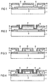
- the pressure sensor according to the prior art shown in FIG. 1 consists of a silicon wafer 1 and a membrane layer of polysilicon located above it. There is a cavity 3 between wafer 1 and membrane 2. The membrane is excited to deflections or vibrations by externally applied pressures or pressure fluctuations. Between wafer and membrane layer are additional layers 4, which are usually formed electrically insulating. On these layers, the membrane lies on the side. Above the membrane auxiliary layers 7 are arranged, which may be, for example, closure layers or planarization layers. During the manufacture of the sensor, a semiconductor circuit likewise arranged on the chip of the sensor can be produced in mask technology. The membrane area of the sensor is then produced together with gate electrodes of MOSFETs, for example.
- a circuit protection layer 8 made of a suitable material, preferably of an oxide or nitride, such as SiO 2 or Si 3 N 4, is located above the arrangement.
- a collar-shaped opening 6 is etched into the micromechanical sensor by etching, wherein the etching process is stopped at the sensor surface. This results in a remaining on the membrane residual structure, which largely determines the mechanical properties of the sensor.
- the openings 6 are made by a dry etching process.
- Figure 2 shows a pressure sensor according to the invention with a Device Protection Layer 9.
- the device protection layer 9 becomes to protect the sensitive flanks, in particular the Layer transitions, and the chip areas, which have the properties determine the component, applied in the region of the opening 6.
- the layer 9 encloses the topological surface structure the sensor so that a perfect seal is effected against external influences.
- the device protection layer 9 can preferably be achieved by applying plasma nitride, Titanium or titanium nitride are produced. By This high quality cover will be more effective Protection of the sensitive layer structure in the area of the opening 6 received. An additional protection of the sensor an external housing can be omitted in principle.
- the micromechanical sensor according to FIG. 3 has a spacer coating 10 on, on the flanks of the openings 6 is applied.
- the spacer coatings 10 cover the Layers lying on the membrane surface only laterally.
- the Spacer coatings can be deposited by depositing a Protective layer, for example of one or more layers containing oxides, titanium, titanium nitride or nitride produce.
- a layer a thin nitride used.
- it will be full-surface or in some areas a layer is deposited on the structure, which projects beyond at least the openings 6.
- an anisotropic Etching for example, without additional use a mask, performed only the edges of the original Layer can stand. All parallel to the wafer surface extending layer parts are thereby removed.
- the remaining, substantially perpendicular to the wafer plane Residues of the coating form the spacer coating 10th
- FIG. 4 represents a combination the method shown in Figure 2 and Figure 3.
- a spacer coating 10 made. This will be topology differences or particularly steep Flanks, such. B. oxide edges, the uniform Bedekkung so balanced that in the second Step, the application of a spacer coating 10 to improved Way can be done.
- the spacer coating leads then to a more resistant to external influences protection of Sensor.
- the method according to the present invention has the advantage that it does not require the use of process steps, not in a conventional process of making CMOS, BiCMOS or bipolar semiconductor structures available stand.
- Another advantage of the invention is that in the production the spacer coating no additional masks in the Comparison to the manufacturing method of the sensor according to FIG. 1 needed.
- micromechanical manufactured according to the embodiments 2 to 4 Sensors are insensitive to external Environmental influences, such as humidity or water, on.
- An additional external encapsulation, an enclosure, or protection of the sensors with a gel may be included omitted micromechanical sensors according to the invention.
Landscapes
- Engineering & Computer Science (AREA)
- Manufacturing & Machinery (AREA)
- Microelectronics & Electronic Packaging (AREA)
- Chemical & Material Sciences (AREA)
- Analytical Chemistry (AREA)
- Physics & Mathematics (AREA)
- General Physics & Mathematics (AREA)
- Pressure Sensors (AREA)
- Measuring Fluid Pressure (AREA)
- Electrostatic, Electromagnetic, Magneto- Strictive, And Variable-Resistance Transducers (AREA)
Description
- Figur 1
- zeigt eine an sich bekannte Ausgestaltung für einen Drucksensor im Querschnitt.
- Figur 2
- zeigt einen erfindungsgemäßen Drucksensor im Querschnitt mit einer Bauelementschutzschicht 9.
- Figur 3
- zeigt eine alternative Ausgestaltung für einen Drucksensor gemäß der Erfindung mit einer Abstandsbeschichtung 10.
- Figur 4
- zeigt eine Ausgestaltung gemäß der Erfindung mit Bauelementschutzschicht 9 und Abstandsbeschichtung 10.
Claims (11)
- Verfahren zur Herstellung eines mikromechanischen Bauelements umfassend die Herstellung eines mikromechanischen Bauelements aus einem Wafer (1), einer Membran (2), einem Hohlraum (3), einer oder mehreren als Auflage für die Membran dienenden Opferschichten (4), welche auf dem Wafer angeordnet sind, Hilfsschichten (7) zur Planarisierung der Bauelementoberfläche und/oder zur Aufnahme von Leiterbahnen oder Halbleiterbauelementen, mindestens einer Öffnung (6), welche eine Verbindung der Umgebung des Bauelements zur Membran herstellt und ggf. einer oder mehreren Schaltungsschutzschichten auf den Hilfsschichten (7),
dadurch gekennzeichnet, daß vor der Vereinzelung des Wafers zu Chips auf das Bauelement mindestens eine Bauelementschutzschicht (9) und/oder Abstandsbeschichtung (10) aufgebracht wird, wobei die Bauelementechutzschicht zumindest die im wesentlichen parallel zur Waferoberfläche verlaufenden und die im wesentlichen senkrecht zur Waferoberfläche verlaufenden Wandungen der Öffnungen abdichtend bedeckt und die Abstandsbeschichtung zumindest die im wesentlichen senkrecht zur Waferoberfläche verlaufenden Wandungen der Öffnungen abdichtend bedeckt. - Verfahren nach Anspruch 1,
dadurch gekennzeichnet, daß die Abstandsbeschichtung (10) hergestellt wird durch die SchritteAufbringen einer oder mehrerer Beschichtungen zumindest in einem parallel zur Waferfläche begrenzten Bereich, wobei der Bereich die Öffnungen (6) überragt und die Beschichtung/-en sich der Kontur der Öffnung weitgehend anpassen,anisotrope Ätzung der aufgebrachten Beschichtung in der Weise, daß die Beschichtung/-en auf den parallel zur Waferoberfläche verlaufenden Flächen entfernt wird/werden. - verfahren zur Herstellung eines mikromechanischen Bauelements nach Anspruch 2,
dadurch gekennzeichnet, daß die Bauelementschutzschicht/-en (9) nach Aufbringen der Abstandsbeschichtung (10) aufgebracht wird/werden, wobei die Bauelementschutzschicht/-en zumindest in einem parallel zur Waferfläche begrenzten, die Öffnungen überragenden Bereich aufgebracht wird/werden und wobei die Bauelementschutzschicht/-en sich der Kontur der Öffnung und der Abstandsbeschichtung weitgehend anpaßt/anpassen. - Mikromechanisches Bauelement umfassend einen Wafer (1), einen oberhalb des Wafers liegenden Hohlraum (3) mit einer darüberliegenden Membran (2), mindestens eine als Auflagefläche für die Membran dienende Opferschicht (4), oberhalb der Membran und des Wafers angeordnete Hilfsshichten (7) zur Planarisierung der Bauelementoberfläche und/oder zur Herstellung von Elementen für eine Halbleiterelektronik, mindestens eine die Membranfläche mit der oberseitigen Umgebung verbindende Öffnung (6) und gegebenenfalls eine oder mehrere Schaltungsschutzschichten oberhalb der Hilfsschichten (7),
dadurch gekennzeichnet, daß die Kontur der Öffnungen (6) mit mindestens einer Bauelementschutzschicht (9) und/oder mindestens einer Abstandsbeschichtung (10) abdichtend bedeckt ist. - Mikromechanisches Bauelement nach Anspruch 4,
dadurch gekennzeichnet, daß der Wafer im wesentlichen aus Silizium besteht. - Mikromechanisches Bauelement nach Anspruch 4 oder 5,
dadurch gekennzeichnet, daß die Membran im wesentlichen aus Polysilizium oder einkristallinem Silizium besteht. - Mikromechanisches Bauelement nach einem der Ansprüche 4 bis 6,
dadurch gekennzeichnet, daß die Hilfsschichten eine Halbleiterschaltung enthalten, wobei die Halbleiterschaltung zur Auswertung oder Ansteuerung des Bauelements dient. - Mikromechanisches Bauelement nach einem der Ansprüche 4 bis 7,
dadurch gekennzeichnet, daß die Schaltungsschutzschicht im wesentlichen aus Oxiden und/oder Nitriden besteht. - Mikromechanisches Bauelement nach einem der Ansprüche 4 bis 8,
dadurch gekennzeichnet, daß die Bauelementschutzschicht mindestens ein Element aus der Gruppe Titan, Titannitrid oder Nitrid enthält. - Mikromechanisches Bauelement nach einem der Ansprüche 4 bis 9,
dadurch gekennzeichnet, daß die Abstandsbeschichtung (10) im wesentlichen aus einem Nitrid besteht. - Verwendung des mikromechanischen Bauelements nach Anspruch 4 für Sensoren.
Applications Claiming Priority (3)
| Application Number | Priority Date | Filing Date | Title |
|---|---|---|---|
| DE19839122A DE19839122A1 (de) | 1998-08-27 | 1998-08-27 | Vor Umwelteinflüssen geschützter mikromechanischer Sensor |
| DE19839122 | 1998-08-27 | ||
| PCT/DE1999/002698 WO2000012987A2 (de) | 1998-08-27 | 1999-08-27 | Vor umwelteinflüssen geschütztes mikromechanisches bauelement |
Publications (2)
| Publication Number | Publication Date |
|---|---|
| EP1108203A2 EP1108203A2 (de) | 2001-06-20 |
| EP1108203B1 true EP1108203B1 (de) | 2005-03-16 |
Family
ID=7878987
Family Applications (1)
| Application Number | Title | Priority Date | Filing Date |
|---|---|---|---|
| EP99953629A Expired - Lifetime EP1108203B1 (de) | 1998-08-27 | 1999-08-27 | Vor umwelteinflüssen geschütztes mikromechanisches bauelement |
Country Status (5)
| Country | Link |
|---|---|
| US (1) | US6401544B2 (de) |
| EP (1) | EP1108203B1 (de) |
| JP (1) | JP3533180B2 (de) |
| DE (2) | DE19839122A1 (de) |
| WO (1) | WO2000012987A2 (de) |
Cited By (1)
| Publication number | Priority date | Publication date | Assignee | Title |
|---|---|---|---|---|
| CN101098569B (zh) * | 2006-06-28 | 2011-06-29 | 歌尔声学股份有限公司 | 半导体传声器芯片 |
Families Citing this family (14)
| Publication number | Priority date | Publication date | Assignee | Title |
|---|---|---|---|---|
| DE19839606C1 (de) * | 1998-08-31 | 2000-04-27 | Siemens Ag | Mikromechanisches Bauelement und Verfahren zu dessen Herstellung |
| US6887732B2 (en) | 2001-05-07 | 2005-05-03 | Applied Materials, Inc. | Microstructure devices, methods of forming a microstructure device and a method of forming a MEMS device |
| US6902656B2 (en) * | 2002-05-24 | 2005-06-07 | Dalsa Semiconductor Inc. | Fabrication of microstructures with vacuum-sealed cavity |
| DE10224790B4 (de) | 2002-06-04 | 2004-10-21 | Infineon Technologies Ag | Beschleunigungssensor und Verfahren zum Herstellen eines Beschleunigungssensors |
| DE10334238A1 (de) * | 2003-07-28 | 2005-02-24 | Robert Bosch Gmbh | Sensoreinlasskanal |
| DE102007013329B4 (de) | 2007-03-20 | 2011-01-27 | Fraunhofer-Gesellschaft zur Förderung der angewandten Forschung e.V. | Verfahren zur Herstellung eines mikromechanischen Bauelements mit einer partiellen Schutzschicht |
| JP2010074523A (ja) * | 2008-09-18 | 2010-04-02 | Rohm Co Ltd | 犠牲層のエッチング方法、memsデバイスの製造方法およびmemsデバイス |
| DE102011002456B4 (de) | 2011-01-05 | 2019-07-18 | Robert Bosch Gmbh | Verfahren zur Herstellung eines mikromechanischen Mikrofonbauelements und so hergestelltes MEMS-Mikrofonbauelement |
| DE102012021413B4 (de) * | 2012-10-30 | 2016-06-02 | Infineon Technologies Ag | Sensor mit Maskierung |
| FR2999805B1 (fr) * | 2012-12-17 | 2017-12-22 | Commissariat Energie Atomique | Procede de realisation d'un dispositif de detection infrarouge |
| CN105329837A (zh) * | 2014-06-03 | 2016-02-17 | 中芯国际集成电路制造(上海)有限公司 | 一种半导体器件及电子装置 |
| FR3072772B1 (fr) * | 2017-10-24 | 2019-10-11 | Mistic | Capteur monolithique integre biocompatible, notamment pour dispositif medical implantable actif |
| DE102020203868B4 (de) | 2020-03-25 | 2022-04-28 | Vitesco Technologies GmbH | Gassensor für ein Fahrzeug |
| DE102020211142B4 (de) | 2020-09-03 | 2022-08-18 | Vitesco Technologies GmbH | Gassensor für ein Fahrzeug |
Family Cites Families (6)
| Publication number | Priority date | Publication date | Assignee | Title |
|---|---|---|---|---|
| JP2729005B2 (ja) * | 1992-04-01 | 1998-03-18 | 三菱電機株式会社 | 半導体圧力センサ及びその製造方法 |
| EP0683921B1 (de) * | 1993-02-04 | 2004-06-16 | Cornell Research Foundation, Inc. | Mikrostrukturen und einzelmask, einkristall-herstellungsverfahren |
| US5427975A (en) * | 1993-05-10 | 1995-06-27 | Delco Electronics Corporation | Method of micromachining an integrated sensor on the surface of a silicon wafer |
| US5914507A (en) * | 1994-05-11 | 1999-06-22 | Regents Of The University Of Minnesota | PZT microdevice |
| DE4418207C1 (de) * | 1994-05-25 | 1995-06-22 | Siemens Ag | Thermischer Sensor/Aktuator in Halbleitermaterial |
| DE69627645T2 (de) * | 1996-07-31 | 2004-02-05 | Stmicroelectronics S.R.L., Agrate Brianza | Integrierter piezoresistiver Druckwandler und Herstellungsverfahren dazu |
-
1998
- 1998-08-27 DE DE19839122A patent/DE19839122A1/de not_active Withdrawn
-
1999
- 1999-08-27 EP EP99953629A patent/EP1108203B1/de not_active Expired - Lifetime
- 1999-08-27 JP JP2000567924A patent/JP3533180B2/ja not_active Expired - Fee Related
- 1999-08-27 WO PCT/DE1999/002698 patent/WO2000012987A2/de not_active Ceased
- 1999-08-27 DE DE59911769T patent/DE59911769D1/de not_active Expired - Lifetime
-
2001
- 2001-02-27 US US09/794,664 patent/US6401544B2/en not_active Expired - Lifetime
Cited By (1)
| Publication number | Priority date | Publication date | Assignee | Title |
|---|---|---|---|---|
| CN101098569B (zh) * | 2006-06-28 | 2011-06-29 | 歌尔声学股份有限公司 | 半导体传声器芯片 |
Also Published As
| Publication number | Publication date |
|---|---|
| US20010054315A1 (en) | 2001-12-27 |
| WO2000012987A2 (de) | 2000-03-09 |
| WO2000012987A3 (de) | 2000-06-22 |
| DE19839122A1 (de) | 2000-03-09 |
| JP3533180B2 (ja) | 2004-05-31 |
| DE59911769D1 (de) | 2005-04-21 |
| EP1108203A2 (de) | 2001-06-20 |
| JP2002523771A (ja) | 2002-07-30 |
| US6401544B2 (en) | 2002-06-11 |
Similar Documents
| Publication | Publication Date | Title |
|---|---|---|
| DE60031089T2 (de) | Kapazitiver Drucksensor und zugehöriges Herstellungsverfahren | |
| EP2170763B1 (de) | Verfahren zur herstellung von leiterbahnbrücken und bauteil mit leitfähiger schicht | |
| DE10321482B4 (de) | Verbesserung von Membraneigenschaften einer Halbleiteranordnung | |
| DE69934841T2 (de) | Druckwandler und Herstellungsverfahren | |
| EP0714017B1 (de) | Kapazitiver Drucksensor | |
| DE4410631A1 (de) | Kapazitiver Sensor bzw. Wandler sowie Verfahren zu dessen Herstellung | |
| EP0721587A1 (de) | Mikromechanische vorrichtung und verfahren zu deren herstellung | |
| EP1108203A2 (de) | Vor umwelteinflüssen geschütztes mikromechanisches bauelement | |
| DE10230166A1 (de) | Elektrischer Kapazitätsdrucksensor mit einer Elektrode mit fester Fläche und Herstellungsverfahren davon | |
| EP1115649B1 (de) | Mikromechanisches bauelement mit verschlossenen membranöffnungen | |
| EP1831662A1 (de) | Mikromechanisches kapazitives sensorelement | |
| DE69403395T2 (de) | Kapazitiver Druckwandler und Herstellungsverfahren dazu | |
| EP0941460B1 (de) | Verfahren zur herstellung von mikromechanischen sensoren | |
| EP0732594A1 (de) | Mikromechanisches Halbleiterbauelement | |
| EP1105344B1 (de) | Mikromechanischer sensor und verfahren zu seiner herstellung | |
| EP1744138B1 (de) | Mikromechanische Vorrichtung mit zwei Sensorstrukturen und Verfahren zur Herstellung einer mikromechanischen Vorrichtung | |
| DE102013102213A1 (de) | Miniaturisiertes Bauelement und Verfahren zur Herstellung | |
| DE19820816A1 (de) | Bondpadstruktur und entsprechendes Herstellungsverfahren | |
| DE4227819C2 (de) | Kapazitiver Drucksensor | |
| WO2000012427A1 (de) | Mikromechanisches bauelement und verfahren zu dessen herstellung | |
| EP0645613B1 (de) | Herstellverfahren für Dünnschicht-Absolutdrucksensoren | |
| DE19851055C2 (de) | Verfahren zur Herstellung von monolithisch integrierten Sensoren | |
| EP0982575A2 (de) | Mikromechanische Struktur | |
| DE102024208643A1 (de) | Kapazitiver Drucksensor mit einer freitragenden Sensierstruktur | |
| DE102018210063A1 (de) | MEMS-Sensor sowie Verfahren zur Herstellung eines MEMS-Sensors |
Legal Events
| Date | Code | Title | Description |
|---|---|---|---|
| PUAI | Public reference made under article 153(3) epc to a published international application that has entered the european phase |
Free format text: ORIGINAL CODE: 0009012 |
|
| 17P | Request for examination filed |
Effective date: 20010215 |
|
| AK | Designated contracting states |
Kind code of ref document: A2 Designated state(s): AT BE CH CY DE DK ES FI FR GB GR IE IT LI LU MC NL PT SE |
|
| RBV | Designated contracting states (corrected) |
Designated state(s): DE FR GB IT NL |
|
| 17Q | First examination report despatched |
Effective date: 20040428 |
|
| GRAP | Despatch of communication of intention to grant a patent |
Free format text: ORIGINAL CODE: EPIDOSNIGR1 |
|
| GRAS | Grant fee paid |
Free format text: ORIGINAL CODE: EPIDOSNIGR3 |
|
| GRAA | (expected) grant |
Free format text: ORIGINAL CODE: 0009210 |
|
| AK | Designated contracting states |
Kind code of ref document: B1 Designated state(s): DE FR GB IT NL |
|
| PG25 | Lapsed in a contracting state [announced via postgrant information from national office to epo] |
Ref country code: NL Free format text: LAPSE BECAUSE OF FAILURE TO SUBMIT A TRANSLATION OF THE DESCRIPTION OR TO PAY THE FEE WITHIN THE PRESCRIBED TIME-LIMIT Effective date: 20050316 Ref country code: GB Free format text: LAPSE BECAUSE OF FAILURE TO SUBMIT A TRANSLATION OF THE DESCRIPTION OR TO PAY THE FEE WITHIN THE PRESCRIBED TIME-LIMIT Effective date: 20050316 |
|
| REG | Reference to a national code |
Ref country code: GB Ref legal event code: FG4D Free format text: NOT ENGLISH |
|
| REG | Reference to a national code |
Ref country code: IE Ref legal event code: FG4D Free format text: GERMAN |
|
| REF | Corresponds to: |
Ref document number: 59911769 Country of ref document: DE Date of ref document: 20050421 Kind code of ref document: P |
|
| NLV1 | Nl: lapsed or annulled due to failure to fulfill the requirements of art. 29p and 29m of the patents act | ||
| GBV | Gb: ep patent (uk) treated as always having been void in accordance with gb section 77(7)/1977 [no translation filed] |
Effective date: 20050316 |
|
| PLBE | No opposition filed within time limit |
Free format text: ORIGINAL CODE: 0009261 |
|
| STAA | Information on the status of an ep patent application or granted ep patent |
Free format text: STATUS: NO OPPOSITION FILED WITHIN TIME LIMIT |
|
| ET | Fr: translation filed | ||
| 26N | No opposition filed |
Effective date: 20051219 |
|
| PGFP | Annual fee paid to national office [announced via postgrant information from national office to epo] |
Ref country code: IT Payment date: 20120821 Year of fee payment: 14 |
|
| PG25 | Lapsed in a contracting state [announced via postgrant information from national office to epo] |
Ref country code: IT Free format text: LAPSE BECAUSE OF NON-PAYMENT OF DUE FEES Effective date: 20130827 |
|
| REG | Reference to a national code |
Ref country code: FR Ref legal event code: PLFP Year of fee payment: 18 |
|
| PGFP | Annual fee paid to national office [announced via postgrant information from national office to epo] |
Ref country code: FR Payment date: 20160822 Year of fee payment: 18 |
|
| PGFP | Annual fee paid to national office [announced via postgrant information from national office to epo] |
Ref country code: DE Payment date: 20161020 Year of fee payment: 18 |
|
| REG | Reference to a national code |
Ref country code: DE Ref legal event code: R119 Ref document number: 59911769 Country of ref document: DE |
|
| REG | Reference to a national code |
Ref country code: FR Ref legal event code: ST Effective date: 20180430 |
|
| PG25 | Lapsed in a contracting state [announced via postgrant information from national office to epo] |
Ref country code: DE Free format text: LAPSE BECAUSE OF NON-PAYMENT OF DUE FEES Effective date: 20180301 |
|
| PG25 | Lapsed in a contracting state [announced via postgrant information from national office to epo] |
Ref country code: FR Free format text: LAPSE BECAUSE OF NON-PAYMENT OF DUE FEES Effective date: 20170831 |