EP1107471B1 - Zeitmultiplex Rake-Finger für WCDMA - Google Patents
Zeitmultiplex Rake-Finger für WCDMA Download PDFInfo
- Publication number
- EP1107471B1 EP1107471B1 EP99309994A EP99309994A EP1107471B1 EP 1107471 B1 EP1107471 B1 EP 1107471B1 EP 99309994 A EP99309994 A EP 99309994A EP 99309994 A EP99309994 A EP 99309994A EP 1107471 B1 EP1107471 B1 EP 1107471B1
- Authority
- EP
- European Patent Office
- Prior art keywords
- symbol
- path
- circuitry
- spreading
- memory
- Prior art date
- Legal status (The legal status is an assumption and is not a legal conclusion. Google has not performed a legal analysis and makes no representation as to the accuracy of the status listed.)
- Expired - Lifetime
Links
Images

Classifications
-
- H—ELECTRICITY
- H04—ELECTRIC COMMUNICATION TECHNIQUE
- H04B—TRANSMISSION
- H04B1/00—Details of transmission systems, not covered by a single one of groups H04B3/00 - H04B13/00; Details of transmission systems not characterised by the medium used for transmission
- H04B1/69—Spread spectrum techniques
- H04B1/707—Spread spectrum techniques using direct sequence modulation
- H04B1/7097—Interference-related aspects
- H04B1/711—Interference-related aspects the interference being multi-path interference
- H04B1/7115—Constructive combining of multi-path signals, i.e. RAKE receivers
- H04B1/7117—Selection, re-selection, allocation or re-allocation of paths to fingers, e.g. timing offset control of allocated fingers
-
- H—ELECTRICITY
- H04—ELECTRIC COMMUNICATION TECHNIQUE
- H04B—TRANSMISSION
- H04B1/00—Details of transmission systems, not covered by a single one of groups H04B3/00 - H04B13/00; Details of transmission systems not characterised by the medium used for transmission
- H04B1/69—Spread spectrum techniques
- H04B1/707—Spread spectrum techniques using direct sequence modulation
- H04B1/7097—Interference-related aspects
- H04B1/711—Interference-related aspects the interference being multi-path interference
- H04B1/7115—Constructive combining of multi-path signals, i.e. RAKE receivers
Definitions
- the present invention relates to the implementation of rake fingers for multi-path components in a spread spectrum communication system.
- So-called rake receivers are currently used to implement the de-spreading function in the receivers of spread spectrum communication systems.
- the receiver is provided with a plurality of identical rake fingers, each one for de-spreading the plurality of multi-path components which may be associated with a transmitted symbol.
- Each rake finger is constructed using identical digital logic, and each finger allocated to a different multi-path component at a different received timing offset.
- the multi-paths are generated by the propagation environment.
- a method of recovering transmitted symbols in the receiver of a spread spectrum system comprising: receiving a signal including multi-path components associated with a transmitted symbol; and de-spreading successive portions of the received signal to provide a symbol estimate based on each multi-path, wherein parts of at least one multi-path of the transmitted symbol is contained in separate portions, the de-spreading step further comprising determining a partial estimate of the transmitted symbol for the at least one multi-path component based on each part of the multi-path contained in each separate portion; and summing said partial estimates.
- the method may further comprise the step, after de-spreading each portion, of storing any partial estimates.
- the method may further comprise the step, on de-spreading each portion, of retrieving any stored partial estimate associated with a multi-path in the current portion.
- the retrieved partial estimate is preferably used in the summing step.
- the method may further include the step of sampling the received signal at successive time intervals thereby generating the successive portions of the received signal.
- the method may further comprise the step of estimating a timing error of the received signal, wherein the successive portions of the received signal are time adjusted to compensate for the timing error prior to de-spreading.
- the successive portions of the received signal may be stored in a sample memory of N samples.
- the successive portions of the received signal may have a length of more than one symbol period.
- the successive portions of the received signal may have a length of two symbol periods.
- the sample memory may be of any size N ⁇ 1. However, as N increases so does the efficiency of the processing.
- circuitry for recovering transmitted symbols in a spread spectrum communication system comprising sample circuitry for receiving a signal including multi-path components associated with a transmitted symbol and de-spreading circuitry for de-spreading successive portions of the received signal to provide a symbol estimate based on each multi-path wherein parts of at least one multi-path of the transmitted symbol are contained in separate portions, the de-spreading circuitry being adapted to determine a partial estimate of the transmitted symbol for the at least one multi-path component based on each part of the multi-path contained in each separate portion; and summing circuitry for summing said partial estimated to produce a full estimate.
- the circuitry may further include a memory for storing the partial estimates, wherein at the end of each successive portion of the received signal any partial estimates are stored in said memory.
- the circuitry may further include a symbol memory, wherein each full estimate is stored in the symbol memory.
- the sample circuitry may include a sample memory, wherein the successive portions of the received signal are stored in the sample memory.
- the circuitry may further include timing error detection and estimation circuitry for determining an error in the timing position of the received signal, wherein the timing position of the received signal is adjusted responsive to said error prior to de-spreading.
- the finger implementation is shared in time for each multi-path.
- Multiple received signals (or calls), each containing multiple multi-paths, may be processed by the inventive technique.
- the invention results in minimum complexity and maximum reuse.
- the time division multiplexed rake finger comprises a sample memory 2 and associated address control circuitry 12, fine timing adjustment circuitry 4, de-spreading circuitry 6, a symbol memory 10 and associated address control circuitry 16, timing error detection and estimation circuitry 14, a control circuit 19, and a finger memory 18.
- the time division multiplexed rake finger 1 is connected to a receive sample bus 20.
- the receive sample data bus 20 carries received signals at the sample rate of the receiver. All data signals and code signals on the receive sample bus may be complex or real.
- the received signals form an input to the time division mulitplexed rake finger 1 on line 22 to the sample memory 2.
- the addressing of the sample memory 2 is controlled by its associated address control circuitry 12 via control and addressing signal lines 26.
- the sample memory inputs the signals on line 22 from the receive sample data bus 20 and outputs signals onto memory output lines 28 which form inputs to the fine timing adjustment circuitry 4. The inputting and outputting of signals to and from the sample memory is discussed in further detail hereinbelow.
- the fine timing adjustment circuitry 4 generates an output signal on line 30 which forms an input to the de-spreading circuit 6.
- the fine timing adjustment circuitry additionally receives signals from the finger memory 18 on lines 44, and inputs signals to the finger memory on lines 45.
- the timing error detection and estimation circuitry 14 receives as an input the signals on line 30 at the output of the fine timing adjustment circuitry 4.
- the timing error detection and estimation circuitry 14 additionally inputs signals to the finger memory 18 on lines 42.
- the de-spreading circuitry 6 receives signals on line 30 from the fine timing adjustment circuitry 4.
- the de-spreading circuitry additionally sends signals to the finger memory 18 on lines 50 and 54 and receives signals from the finger memory on lines 44, 48 and 52.
- the de-spreading circuitry 6 generates an output on line 34.
- the symbol memory 10 receives the signals from the de-spreading circuitry 6 on line 34 as an input, and generates an output on line 36. The inputting and outputting of signals to and from the symbol memory is controlled by the address control circuitry 16 via signal lines 38.
- the control circuit 19 generates control signals on a bus 21 for controlling the operation of the time division multiplexed rake finger 1.
- the control circuit 19 communicates via signal lines (not shown) with the outside world, for example a digital signal processor, as will be understood by one skilled in the art.
- the sample memory is controlled by the address control circuitry 12 to input a sample, or portion, of the received signals on the receive sample bus 20.
- the received signals at the sample rate of the receiver on the receive sample data bus 20 comprise symbols associated with callers. Information, or symbols, from several callers may be present on the receive sample data bus 20. Multi-paths for each symbol may be present.
- a sample of the receive sample data bus 20 is taken at regular intervals.
- the sample will capture the signals on the receive sample data bus over a particular, fixed, time period.
- Each captured sample contains N received signal samples.
- the sample memory may contain multiple entries of captured samples where each entry is from a different source, e.g. antennas within a sector or different sectors as would be familiar to one skilled in the art of mobile cellular communications.
- Each captured sample is then processed in the receiver to recover the transmitted signals, as will be described further hereinbelow.
- Each captured sample may contain partial, full, or multiple symbols from one or more callers, and may contain partial or full multi-paths of one or more symbols.
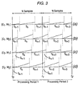
- the invention is hereafter described with reference to a particular embodiment in which the sample of the received signal that is taken, which is written to the sample memory, is equivalent in length to the time period of two transmitted symbols.
- the sample is a two-symbol period sample.
- a single symbol corresponds to 256 chip time periods, and thus the sample that is written into the sample memory corresponds to a sample length of 512 chip time periods.
- the 512 chip period sample commences at time t0 and ends at time t1.
- the second two symbol period sample written into the sample memory 2 in the next sample period.
- the second 512 chip period sample commences at time t1 and ends at time t2.
- the time period t0 to t1 represents a first processing period
- the time period t1 to t2 represents a second processing period.
- Each of the first and second processing periods contains N samples.
- Figure 3(a) illustrates the first multi-path of the first caller, [C1,M1].
- Figure 3(b) illustrates the second multi-path of the first caller, [C1, M2].
- Figure 3(c) illustrates the first multi-path of the second caller, [C2, M1].
- Figure 3(d) illustrates the second multi-path of the second caller, [C2, M2].
- the four multi-paths shown in Figures 3(a) to 3(d) are representative of the multi-paths which are present, and are sufficient for to provide an understanding of the present invention.
- each sample period corresponds to the length of two symbols, there are potentially two transmitted symbols in the captured sample.
- the sample will not be synchronised to the start of a particular symbol. So, as shown for example in Figure 3(a), at time t0 the last portion of a symbol associated with the (n-1)th symbol of the first multi-path of the first caller is received. The nth symbol Sn of the first multi-path of the first caller is then received in full. Then finally the first part of the (n+1)th symbol of the first multi-path of the first caller is received.
- the first sample written into the memory in the first processing period include two partial symbols and one full symbol of the first multi-path of the first caller.
- full and partial symbols are stored in the memory, as exemplified by Figures 3(b) to 3(d).
- the timing error detection and estimation circuitry 14 performs operations on the signals output by the fine timing adjustment circuitry 4 to estimate the location of the start point of all the symbols of the first caller shown in Figure 3(a), and its corresponding multi-paths.
- the estimate of the starting position for symbols and multi-paths of a particular caller may be recalculated and re-estimated on a regular basis.
- timing circuit is shown here for the purpose of illustration. It may or may not be included in an implementation of the invention. In the case of non-inclusion the timing information is provided by a separate source that has the same format as described herein.
- the timing error detection and estimation circuitry 14 generates a fractional error timing signal and a coarse or integer error timing signal.
- the fractional error timing signal represents the amount, by less than a chip period, that the symbol estimate must be adjusted by
- the integer error timing signal represents the amount, by multiples of a chip period, that the symbol estimate must be adjusted by.
- the finger memory has a context associated with each multi-path of each caller.
- the timing error information (both fractional and integer) associated with each multi-path of each caller is stored with the appropriate context in the finger memory.
- timing error detection and estimation circuitry 14 will be apparent to one skilled in the art.
- the address control circuitry 12 reads stored sample data from the memory, and presents it on lines 28 to the fine timing adjustment circuitry 4.
- the address control circuitry controls the sample memory to provide the full two-symbol period sample of Figure 3(a) to the fine timing adjustment circuitry.
- the two symbol period sample contains, as discussed hereinabove, various multi-paths for various callers as shown by way of example in the first processing period of Figures 3(a) to 3(d).
- the finger memory 18 is controlled by the control circuit 19 to switch between contexts in accordance with the multi-path currently being processed.
- the fine timing adjustment circuitry uses the fractional error timing information generated by the timing error detection and estimation circuitry and stored in the finger memory 18 to fractionally adjust the timing of each multi-path in the given processing period.
- the control circuit 19 controls the finger memory 18 to switch its context to output on lines 44 to the fine timing adjustment circuitry 4 the fractional timing information associated with the first multi-path of the first caller.
- the fine timing adjustment circuitry 4 adjusts the fine timing of the first multi-path of the first caller as shown in Figure 3(a) in accordance with this timing information.
- the control circuit 19 then switches the context of the finger memory 18 to output the fractional timing information associated with the second multi-path of the first caller on line 44, to thereby adjust the fractional timing of the signal shown in Figure 3(b).
- the context of the finger memory 18 is switched to provide the necessary fractional timing information on line 44 for each of the other multi-paths to be processed for each caller.
- the signal on line 28 at the input to the fine timing adjustment circuitry 4 has a rate of at least two samples per chip. This is necessary to obtain a sample of the received signal which corresponds to the centre of the chip period. This ensures that the subsequent de-spreading operation will produce the maximum signal to noise ratio as the correlation gain is maximised. If the number of samples is low, for example two, an interpolator is necessary. If the number of samples is higher an interpolator may not be necessary, because one of the samples is more likely to approximate the peak. A sample selector may then be used. Regardless of the implementation, the output of the fine timing adjustment circuitry 4 on line 30 has a rate of one sample per chip.
- the fine-time adjusted samples are then provided to the de-spreading circuitry 6 via line 30.
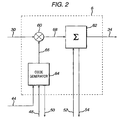
- An example implementation of the de-spreading circuitry 6 is shown in Figure 2.
- the de-spreading circuitry of Figure 2 includes a multiplier 60, a code generator 64 and a summer 62.
- the code generator 64 receives the timing signals from the finger memory 18 on line 44, and receives and transmits de-spreading code information on lines 48 and 50 between the de-spreading circuitry 6 and the finger memory 18.
- the code generator is loaded, from finger memory 18 with the spreading code known to be used by the first caller via lines 48.
- the finger memory stores the spreading codes for the different callers. Thus each context in the finger memory 18 will additionally be associated with a spreading code. Under the control of the control circuit 19, the finger memory outputs the appropriate spreading code for the current context on line 48.
- the finger memory outputs the integer timing error information associated with that context, and as discussed above stored in the finger memory, on line 44 to the de-spreading circuitry 6.
- the code generator 64 then uses the timing information on line 44 to shift the spreading code on line 48 by the necessary amount to be in the estimated same time frame as the multi-path currently being processed.
- the appropriate context is selected in the finger memory 18, and the timing information output on line 44 and the spreading code output on line 48.
- the context in the finger memory is thereafter switched to the context for the second multi-path of the first caller, and the appropriate information output on lines 44 and 48. Thereafter, the context is switched to the context for the first multi-path of the second caller, and then the second multi-path of the second caller.
- the time shifted spreading code is output on line 66 to the multiplier, and multiplied with the fractional time-shifted sample from the sample memory 2 on line 30.
- the de-spread signal is then output on line 68 from the multiplier 60 and provided to the summer 62.
- the summer sums the de-spread signal to give a first estimate at the receiver of the transmitted symbol based on the first multi-path.
- the summed result for each multi-path of each caller, comprising the estimate is output on line 34 to the symbol memory 10.
- the de-spread signal on line 34 comprises a received symbol, or partial symbol, at the symbol rate.
- a symbol boundary will not coincide with the end of a processing period the content of the summer 62 is stored in the finger memory at the end of the partial symbol using lines 54, and then reinstated when that multi-path is to be next processed using lines 52.
- the partial summed result for a partial symbol is stored in the finger memory in association with the context associated with that multi-path.
- control circuit 19 For every sample output from the sample memory 2 the control circuit 19, which includes counters, counts the total number of chip periods elapsed and the number of chip periods elapsed for the current symbol.
- the control circuit 19 counts the number of chips input by the de-spreading circuitry 6 from the start of the particular multi-path being processed. For the nth symbol of the first multi-path of the first caller, as shown in Figure 3(a), the control circuit 19 will count-up 256 chip periods before the end of the current two-chip period sample is reached.
- the de-spreading circuitry de-spreads the symbols in successive multi-paths for successive calls.
- the first multi-path associated with the nth symbol is fully contained within the sample period of Figure 3(a).
- the time multiplexed rake finger proceeds to process the first multi-path of the (n+1)th symbol from the first caller, which is identified as being the next received sample.
- the sample is provided to the fine timing adjustment circuitry and then to the de-spreading circuitry, with the appropriate timing information being provided on lines 44.
- the first sample stored in the sample memory includes only part of the (n+1)th symbol of the first multi-path of the first caller.
- the de-spreading circuitry performs a partial de-spreading of the (n+1)th symbol based on the portion of the symbol that is available.
- the result of the partial de-spreading of the (n+1)th symbol of the first multi-path of the first caller is output on line 54 to the finger memory.
- This partial result is stored in the finger memory in association with the context corresponding to the (n+1)th symbol of the first multi-path of the first caller.
- the unused portion of the spreading code in the code generator 64 is stored in the finger memory via lines 50 in association with the context.
- the finger memory will additionally include partial de-spreading results associated with the second multi-path of the (n+1)th symbol of the first caller, the first multi-path of the (n+1)th symbol of the second caller, and the second multi-path of the (n+1)th symbol of the second caller.
- the contents of the registers of the de-spreading circuitry are thus stored in the finger memory 18 with an association to the appropriate symbol of the appropriate multi-path of the appropriate caller.
- the control circuit 19 counts the number of chip periods processed for each partially de-spread symbol, and this value is stored in the finger memory 18 along with an association to the appropriate context.
- the second processing period includes, referring to Figure 3(a), the final portion of the (n+1)th symbol of the first multi-path of the first caller, referring to Figure 3(b) the final portion of the (n+1)th symbol of the second multi-path of the first caller, referring to Figure 3(c) the final portion of the (n+1)th symbol of the first multi-path of the second caller, and referring to Figure 3(d) the final portion of the (n+1)th symbol of the second multi-path of the second caller.
- the two-symbol sample period including all the multi-paths of all callers of the second processing period is transferred on line 28 to the fine timing adjustment circuitry 4.
- the first multi-path of the first caller in the second processing period is processed.
- the first part of this multi-path is the final portion of the (n+1)th symbol, the first part of which was processed in the first processing period.
- the fractional timing information stored in the finger memory for the first multi-path of the first caller is output on line 44 to the fine timing adjusted circuitry 4, and the thus time adjusted sample output on line 30.
- the context in the finger memory is changed for the processing of the second multi-path of the first caller, the first multi-path of the second caller, and the second multi-path of the second caller.
- the thus time adjusted multi-paths are then de-spread in the de-spreading circuitry 6.
- the first symbol to be de-spread is the last portion of the (n+1)th symbol.
- the partial result formulated in the previous processing period and stored in the finger memory needs to be used.
- the context of the finger memory 18 is switched to the (n+1)th symbol of the first multi-path of the first caller, and the stored information associated with that context output form the finger memory on lines 44 and 52.
- the stored integer timing information is provided to the code generator 64.
- the remanding portion of the spreading code for the symbol is provided on line 48 to the code generator 64.
- the partially summed result from the previous processing period is provided on line 52 and loaded in the summer 62.
- the control circuit 19 is loaded with the counter values for the (n+1)th symbol of the first multi-path of the first caller which is also previously stored in the finger memory 18 in association with the corresponding context.
- the de-spreading circuitry de-spreads the final portion of the first multi-path of the (n+1)th symbol of the first caller and outputs the final summed value on line 34, and presented for storage in the symbol memory 10.
- the remainder of the two-sample period of the first multi-path of the first caller is then processed.
- the (n+2)th symbol is processed in the same way as the nth symbol in the first processing period.
- the (n+3)th partial symbol is processed in the same way as the (n+1)th partial symbol in the first processing period.
- the completed multi-path symbol estimates output on line 34 from the de-spreading circuitry are stored in the symbol memory 10 under the control of the address control circuitry, which is in turn controlled by the control circuitry 19.
- the multi-path symbol estimates stored in the symbol memory 10 are subsequently read out onto line 36 under the control of the address control circuitry 16 for further processing, such as the combining of multi-paths associated with the same symbol (maximum ratio combining).
- the time division multiplexed rake finger uses a sample memory, or buffer, which stores only two minimum rate symbol periods of signal data.
- a typical use of the invention may be in the implementation of a rake receiver for wireless CDMA cellular systems such as Universal Mobile Telecommunications Standard (UMTS).
- UMTS Universal Mobile Telecommunications Standard
- the minimum rate symbol period of signal data is 256 chip periods.
- UMTS uses a variable spreading code. Therefore other numbers of complete symbols could be received in a 512 chip time period in addition to the two partial symbols. For example there are symbols which are only 32 or 64 chip periods long.
- time division multiplexed rake finger of Figure 1 is duplicated, because the received signals are complex and therefore there are two processing 'legs': one for the I channel and one for the Q channel.
- the finger memory 18 can be considered to comprise n finger memories, corresponding to the n fingers which would normally be required, each associated with one of n multi-paths.
- the updating of the register values in the time division multiplexed rake finger from the memory 18 is termed context switching.
- the secondary summing function provided by the context switching of the contents of the de-spreading circuitry 6 solves the problem of the received signal in the sample memory being rarely synchronised with the received signal symbol timing. Even if one multi-path had time alignment between the received signal and the sample memory, the other multi-paths would not.
- the primary benefit of the time division multiplexed rake finger according to the invention is its low hardware complexity relative to the implementation of multiple rake receivers each with multiple fingers.
- the time division multiplexing may be used for multiple channels (or multiple callers), the limit being dependent on the number of fingers used for each channel and the processing clock rate. This gives a distinct advantage as channel elements which are designed for high rate channels may also be used to process multiple low rate channels, hence improving efficiency significantly in terms of both hardware implementation cost and occupied area.
- the time division multiplexed rake finger of the invention allows considerable flexibility over conventional designs as the fingers may be assigned dynamically dependent on the number of multi-paths present on a call at a particular instant in time.
- N f Int [ N . fp / ( ( N + N p ) * rc ) ] where Int[.] is the integer part of the argument.
- Nf 23.
- 8 fingers can be considered to be satisfactory. This particular scenario enables almost 3 channels (8+8+7 fingers) to be supported.
- the structure shown in Figure 1 consists of an input signal bus 20 which feeds the sample memory 2.
- the sample memory may be a dual port RAM (DPRAM) or a static RAM (SRAM) which operates at double rate to allow both read and write cycles from the same port (or address and data bus).
- DPRAM dual port RAM
- SRAM static RAM
- Such a RAM may be implemented as two blocks of SRAM (one each for read and write cycles which are interchanged at the end of each processing period) or as a single DPRAM.
- the sample RAM size in bits is N x the number of sources (antennas) x 2 buffers x L samples per chip period x B bits per signal sample x 2 (I/Q).
- TS time-slot
- the memory size for the receive sample buffer is significantly smaller than that which would be required for frame period processing (typically 1M byte) or timeslot processing (typically 61.44kbytes).
- the memory size for the symbol buffer is typically dimensioned for timeslot processing
Landscapes
- Engineering & Computer Science (AREA)
- Computer Networks & Wireless Communication (AREA)
- Signal Processing (AREA)
- Synchronisation In Digital Transmission Systems (AREA)
- Mobile Radio Communication Systems (AREA)
Claims (15)
- Verfahren zum Wiederherstellen übertragener Symbole in dem Empfänger eines Spreizspektrumsystems, mit den folgenden Schritten: Empfangen (2) eines Signals mit Mehrwegekomponenten in Assoziation mit einem übertragenen Symbol; und Entspreizen (6) sukzessiver Teile des empfangenen Signals, um auf der Basis jedes Mehrfachweges eine Symbolschätzung bereitzustellen, wobei Teile mindestens eines Mehrfachweges des übertragenen Symbols in separaten Anteilen enthalten sind, wobei der Schritt des Entspreizens (6) ferner umfaßt, eine partielle Schätzung des übertragenen Symbols für die mindestens eine Mehrwegekomponente auf der Basis jedes Teils des Mehrfachweges, der in jedem separaten Anteil enthalten ist, zu bestimmen; und Summieren (62) der partiellen Schätzungen.
- Verfahren nach Anspruch 1, ferner mit dem Schritt des Speicherns (18, 54) etwaiger partieller Schätzungen nach dem Entspreizen jedes Anteils.
- Verfahren nach Anspruch 2, mit dem Schritt des Abrufens einer etwaigen gespeicherten partiellen Schätzung (18, 52) in Assoziation mit einem Mehrfachweg in dem aktuellen Anteil beim Entspreizen jedes Anteils.
- Verfahren nach Anspruch 3, wobei die abgerufene partielle Schätzung (52) in dem Summierschritt (62) benutzt wird.
- Verfahren nach einem der Ansprüche 1 bis 4, ferner mit dem Schritt des Abtastens des empfangenen Signals in sukzessiven zeitintervallen, wodurch die sukzessiven Anteile des empfangenen Signals erzeugt werden.
- Verfahren nach einem der Ansprüche 1 bis 5, ferner mit dem Schritt des Schätzens (14) eines Zeitfehlers (42) des empfangenen Signals, wobei die sukzessiven Anteile des empfangenen Signals zeitlich eingestellt werden (4, 44, 30), um den Zeitfehler vor dem Entspreizen (6) auszugleichen.
- Verfahren nach einem der Ansprüche 1 bis 7, wobei die sukzessiven Anteile des empfangenen Signals in einem Abtastwertspeicher (2) gespeichert werden:
- Verfahren nach einem der Ansprüche 1 bis 7, wobei die sukzessiven Anteile des empfangenen Signals eine Länge von mehr als einer Symbolperiode aufweisen.
- Verfahren nach Anspruch 8, wobei die sukzessiven Anteile des empfangenen Signals eine Länge von zwei Symbolperioden aufweisen.
- Verfahren nach einem der Ansprüche 1 bis 7, wobei die sukzessiven Anteile des empfangenen Signals eine Länge von weniger als einer Symbolperiode aufweisen.
- Schaltkreise zum Wiederherstellen übertragener Symbole in einem Spreizspektrumsystem, mit Abtastschaltkreisen (2) zum Empfangen eines Signals mit Mehrwegekomponenten in Assoziation mit einem übertragenen Symbol und Entspreizungsschaltkreisen (6) zum Entspreizen sukzessiver Teile des empfangenen Signals, um auf der Basis jedes Mehrfachweges eine Symbolschätzung bereitzustellen, wobei Teile mindestens eines Mehrfachweges des übertragenen Symbols in separaten Anteilen enthalten sind, wobei die Entspreizungsschaltkreise (6) ferner so ausgelegt sind, daß sie eine partielle Schätzung des übertragenen Symbols für die mindestens eine Mehrwegekomponente auf der Basis jedes Teils des Mehrfachweges, der in jedem separaten Anteil enthalten ist, bestimmen; und Summierschaltkreise (62) zum Summieren der partiellen Schätzungen, um eine volle Schätzung zu produzieren.
- Schaltkreise nach Anspruch 11, ferner mit einem Speicher (18) zum Speichern der partiellen Schätzungen nach dem Entspreizen jedes Anteils.
- Schaltkreise nach Anspruch 11 oder Anspruch 12, ferner mit einem Symbolspeicher (10), wobei jede volle Schätzung in dem Symbolspeicher gespeichert wird.
- Schaltkreise nach einem der Ansprüche 11 bis 13, wobei die Abtastschaltkreise (2) einen Abtastwertspeicher (2) enthalten, wobei die sukzessiven Anteile des empfangenen Signals in einem Abtastwertspeicher gespeichert werden.
- Schaltkreise nach einem der Ansprüche 11 bis 14, ferner mit Zeitfehlerdetektions- und Schätzschaltkreisen (14) zum Bestimmen eines Fehlers in der Zeitposition des empfangenen Signals, wobei die Zeitposition des empfangenen Signals als Reaktion auf den Fehler vor dem Entspreizen eingestellt wird (4, 44, 30).
Priority Applications (3)
| Application Number | Priority Date | Filing Date | Title |
|---|---|---|---|
| DE69930224T DE69930224T2 (de) | 1999-12-10 | 1999-12-10 | Zeitmultiplex Rake-Finger für WCDMA |
| EP99309994A EP1107471B1 (de) | 1999-12-10 | 1999-12-10 | Zeitmultiplex Rake-Finger für WCDMA |
| US09/729,900 US6954487B2 (en) | 1999-12-10 | 2000-12-05 | Time division multiplexed rake finger for W-CDMA |
Applications Claiming Priority (1)
| Application Number | Priority Date | Filing Date | Title |
|---|---|---|---|
| EP99309994A EP1107471B1 (de) | 1999-12-10 | 1999-12-10 | Zeitmultiplex Rake-Finger für WCDMA |
Publications (2)
| Publication Number | Publication Date |
|---|---|
| EP1107471A1 EP1107471A1 (de) | 2001-06-13 |
| EP1107471B1 true EP1107471B1 (de) | 2006-03-08 |
Family
ID=8241806
Family Applications (1)
| Application Number | Title | Priority Date | Filing Date |
|---|---|---|---|
| EP99309994A Expired - Lifetime EP1107471B1 (de) | 1999-12-10 | 1999-12-10 | Zeitmultiplex Rake-Finger für WCDMA |
Country Status (3)
| Country | Link |
|---|---|
| US (1) | US6954487B2 (de) |
| EP (1) | EP1107471B1 (de) |
| DE (1) | DE69930224T2 (de) |
Families Citing this family (11)
| Publication number | Priority date | Publication date | Assignee | Title |
|---|---|---|---|---|
| GB2357406B (en) * | 1999-12-14 | 2004-01-21 | Nokia Mobile Phones Ltd | Combiner |
| JP3871540B2 (ja) * | 2001-10-05 | 2007-01-24 | 富士通株式会社 | 受信装置および半導体装置 |
| US7023902B2 (en) * | 2001-11-06 | 2006-04-04 | Qualcomm Inc. | Apparatus and method for scalable offline CDMA demodulation |
| US7649860B2 (en) | 2002-01-31 | 2010-01-19 | Qualcomm Incorporated | Buffer-based GPS and CDMA pilot searcher |
| US7463671B2 (en) * | 2002-02-19 | 2008-12-09 | Marvell World Trade Ltd. | Rake receiver interface |
| US7596134B2 (en) * | 2002-07-03 | 2009-09-29 | Freescale Semiconductor, Inc. | Flexible method and apparatus for performing digital modulation and demodulation |
| US7675963B2 (en) * | 2002-07-29 | 2010-03-09 | Infineon Technologies Ag | Method and device for passing parameters to rake receiver |
| US7680083B2 (en) * | 2005-07-28 | 2010-03-16 | Broadcom Corporation | Rake receiver architecture within a WCDMA terminal |
| US8064414B2 (en) * | 2005-12-13 | 2011-11-22 | Qualcomm, Incorporated | Range extension techniques for a wireless local area network |
| US7839917B2 (en) * | 2006-09-18 | 2010-11-23 | Mediatek Inc. | Receiver of a CDMA system with a path alignment circuit |
| CN102421186B (zh) * | 2011-01-24 | 2014-04-02 | 展讯通信(上海)有限公司 | 一种冲击响应定时调整方法及装置 |
Family Cites Families (9)
| Publication number | Priority date | Publication date | Assignee | Title |
|---|---|---|---|---|
| US5506861A (en) * | 1993-11-22 | 1996-04-09 | Ericsson Ge Mobile Comminications Inc. | System and method for joint demodulation of CDMA signals |
| FI943249A (fi) * | 1994-07-07 | 1996-01-08 | Nokia Mobile Phones Ltd | Menetelmä vastaanottimen ohjaamiseksi ja vastaanotin |
| GB2293730B (en) * | 1994-09-28 | 1998-08-05 | Roke Manor Research | Apparatus for use in equipment providing a digital radio link between a fixed and a mobile radio unit |
| JP2820918B2 (ja) * | 1996-03-08 | 1998-11-05 | 株式会社ワイ・アール・ピー移動通信基盤技術研究所 | スペクトル拡散通信装置 |
| JPH09321667A (ja) * | 1996-05-29 | 1997-12-12 | Yozan:Kk | Cdma通信システム用受信機 |
| US5953382A (en) * | 1996-07-17 | 1999-09-14 | Asano; Nobuo | CDMA system mobile communication receiver |
| JPH10200444A (ja) * | 1997-01-06 | 1998-07-31 | Sony Corp | 受信装置、受信方法、無線システムの端末装置 |
| JPH10209919A (ja) * | 1997-01-21 | 1998-08-07 | Sony Corp | 受信装置及び受信方法、並びに携帯電話システムの端末装置 |
| US6618431B1 (en) * | 1998-12-31 | 2003-09-09 | Texas Instruments Incorporated | Processor-based method for the acquisition and despreading of spread-spectrum/CDMA signals |
-
1999
- 1999-12-10 EP EP99309994A patent/EP1107471B1/de not_active Expired - Lifetime
- 1999-12-10 DE DE69930224T patent/DE69930224T2/de not_active Expired - Lifetime
-
2000
- 2000-12-05 US US09/729,900 patent/US6954487B2/en not_active Expired - Lifetime
Also Published As
| Publication number | Publication date |
|---|---|
| DE69930224T2 (de) | 2006-12-14 |
| US6954487B2 (en) | 2005-10-11 |
| US20010036195A1 (en) | 2001-11-01 |
| EP1107471A1 (de) | 2001-06-13 |
| DE69930224D1 (de) | 2006-05-04 |
Similar Documents
| Publication | Publication Date | Title |
|---|---|---|
| KR100938022B1 (ko) | 통신 시스템에서 수신 신호를 처리하기 위한 방법 및 장치 | |
| US6385259B1 (en) | Composite code match filters | |
| EP1107471B1 (de) | Zeitmultiplex Rake-Finger für WCDMA | |
| US6947470B2 (en) | Rake receiver for a CDMA system, in particular incorporated in a cellular mobile phone | |
| JP2734952B2 (ja) | Cdma基地局受信装置 | |
| JP4720658B2 (ja) | 同期検出回路およびマルチモード無線通信装置 | |
| US6980587B2 (en) | Method for acquisition of slot timing in a direct sequence spread spectrum communication receiver | |
| KR101157108B1 (ko) | 메모리 아키텍처를 사용하여 1차 셀을 검색하기 위한 상관기 | |
| EP1075090B1 (de) | Ein CDMA Demodulationsverfahren und Demodulator | |
| EP1300961B1 (de) | Empfangseinhet und Halbleitervorrichtung | |
| US7023902B2 (en) | Apparatus and method for scalable offline CDMA demodulation | |
| EP1561288B1 (de) | Auf Speicher basierende Vorrichtung und Verfahren zur Kanalschätzung in einem digitalen Kommunikationsempfänger | |
| US7099376B2 (en) | Method for parallel type interference cancellation in code division multiple access receiver | |
| EP0905888A2 (de) | Verfahren zur Korrelationsdetektion und anpgepasstes Filter | |
| EP1416650A1 (de) | Anfangssynchronisationssuche in einem Mobilfunksystem | |
| US6959035B2 (en) | Post-correlation interpolation for delay locked loops | |
| US20030012269A1 (en) | receiving apparatus and reception timing estimation method | |
| JP3398708B2 (ja) | スペクトル拡散受信装置 | |
| KR100320828B1 (ko) | 정합필터및그를이용한기지국장치및이동국장치,타이밍검출방법과rake합성방법 | |
| EP1416352A1 (de) | Verfahren und Vorrichtung zur effizienten Matrixmultiplizierung in einem Direktsequenzspreizspektrumkommunikationsystem | |
| EP1532748B1 (de) | Verzögerungsleitung für den Empfang von Mehrfachausbreitungswegen | |
| KR100430527B1 (ko) | 채널 추정 지연 보상이 가능한 레이크 수신기 | |
| EP1364471B1 (de) | Multicode rake empfänger in einer mobilstation | |
| KR20020014531A (ko) | 이동통신시스템의 레이크 수신장치 및 방법 | |
| KR20020031667A (ko) | 순차 다중경로 신호합침을 이용한 무선 이동통신 시스템의다중경로 수신기 및 다중경로 수신방법 |
Legal Events
| Date | Code | Title | Description |
|---|---|---|---|
| PUAI | Public reference made under article 153(3) epc to a published international application that has entered the european phase |
Free format text: ORIGINAL CODE: 0009012 |
|
| AK | Designated contracting states |
Kind code of ref document: A1 Designated state(s): DE ES FR GB IT |
|
| AX | Request for extension of the european patent |
Free format text: AL;LT;LV;MK;RO;SI |
|
| 17P | Request for examination filed |
Effective date: 20011129 |
|
| AKX | Designation fees paid |
Free format text: DE ES FR GB IT |
|
| 17Q | First examination report despatched |
Effective date: 20050427 |
|
| GRAP | Despatch of communication of intention to grant a patent |
Free format text: ORIGINAL CODE: EPIDOSNIGR1 |
|
| GRAS | Grant fee paid |
Free format text: ORIGINAL CODE: EPIDOSNIGR3 |
|
| GRAA | (expected) grant |
Free format text: ORIGINAL CODE: 0009210 |
|
| AK | Designated contracting states |
Kind code of ref document: B1 Designated state(s): DE ES FR GB IT |
|
| PG25 | Lapsed in a contracting state [announced via postgrant information from national office to epo] |
Ref country code: IT Free format text: LAPSE BECAUSE OF FAILURE TO SUBMIT A TRANSLATION OF THE DESCRIPTION OR TO PAY THE FEE WITHIN THE PRESCRIBED TIME-LIMIT;WARNING: LAPSES OF ITALIAN PATENTS WITH EFFECTIVE DATE BEFORE 2007 MAY HAVE OCCURRED AT ANY TIME BEFORE 2007. THE CORRECT EFFECTIVE DATE MAY BE DIFFERENT FROM THE ONE RECORDED. Effective date: 20060308 |
|
| REG | Reference to a national code |
Ref country code: GB Ref legal event code: FG4D |
|
| REF | Corresponds to: |
Ref document number: 69930224 Country of ref document: DE Date of ref document: 20060504 Kind code of ref document: P |
|
| PG25 | Lapsed in a contracting state [announced via postgrant information from national office to epo] |
Ref country code: ES Free format text: LAPSE BECAUSE OF FAILURE TO SUBMIT A TRANSLATION OF THE DESCRIPTION OR TO PAY THE FEE WITHIN THE PRESCRIBED TIME-LIMIT Effective date: 20060619 |
|
| ET | Fr: translation filed | ||
| PLBE | No opposition filed within time limit |
Free format text: ORIGINAL CODE: 0009261 |
|
| STAA | Information on the status of an ep patent application or granted ep patent |
Free format text: STATUS: NO OPPOSITION FILED WITHIN TIME LIMIT |
|
| 26N | No opposition filed |
Effective date: 20061211 |
|
| REG | Reference to a national code |
Ref country code: FR Ref legal event code: CD Owner name: ALCATEL-LUCENT USA INC. Effective date: 20131122 |
|
| REG | Reference to a national code |
Ref country code: FR Ref legal event code: GC Effective date: 20140410 |
|
| REG | Reference to a national code |
Ref country code: FR Ref legal event code: RG Effective date: 20141015 |
|
| REG | Reference to a national code |
Ref country code: FR Ref legal event code: PLFP Year of fee payment: 17 |
|
| REG | Reference to a national code |
Ref country code: FR Ref legal event code: PLFP Year of fee payment: 18 |
|
| PGFP | Annual fee paid to national office [announced via postgrant information from national office to epo] |
Ref country code: GB Payment date: 20161222 Year of fee payment: 18 Ref country code: DE Payment date: 20161213 Year of fee payment: 18 |
|
| PGFP | Annual fee paid to national office [announced via postgrant information from national office to epo] |
Ref country code: FR Payment date: 20161222 Year of fee payment: 18 |
|
| REG | Reference to a national code |
Ref country code: DE Ref legal event code: R119 Ref document number: 69930224 Country of ref document: DE |
|
| GBPC | Gb: european patent ceased through non-payment of renewal fee |
Effective date: 20171210 |
|
| REG | Reference to a national code |
Ref country code: FR Ref legal event code: ST Effective date: 20180831 |
|
| PG25 | Lapsed in a contracting state [announced via postgrant information from national office to epo] |
Ref country code: DE Free format text: LAPSE BECAUSE OF NON-PAYMENT OF DUE FEES Effective date: 20180703 Ref country code: FR Free format text: LAPSE BECAUSE OF NON-PAYMENT OF DUE FEES Effective date: 20180102 |
|
| PG25 | Lapsed in a contracting state [announced via postgrant information from national office to epo] |
Ref country code: GB Free format text: LAPSE BECAUSE OF NON-PAYMENT OF DUE FEES Effective date: 20171210 |
|
| REG | Reference to a national code |
Ref country code: DE Ref legal event code: R081 Ref document number: 69930224 Country of ref document: DE Owner name: WSOU INVESTMENTS, LLC, LOS ANGELES, US Free format text: FORMER OWNER: LUCENT TECHNOLOGIES INC., MURRAY HILL, N.J., US |