EP1098361A2 - Particle material, anisotropic conductive connection and anisotropic conductive connection material - Google Patents
Particle material, anisotropic conductive connection and anisotropic conductive connection material Download PDFInfo
- Publication number
- EP1098361A2 EP1098361A2 EP00123648A EP00123648A EP1098361A2 EP 1098361 A2 EP1098361 A2 EP 1098361A2 EP 00123648 A EP00123648 A EP 00123648A EP 00123648 A EP00123648 A EP 00123648A EP 1098361 A2 EP1098361 A2 EP 1098361A2
- Authority
- EP
- European Patent Office
- Prior art keywords
- anisotropic conductive
- insulating
- conductive connection
- particle
- resin layer
- Prior art date
- Legal status (The legal status is an assumption and is not a legal conclusion. Google has not performed a legal analysis and makes no representation as to the accuracy of the status listed.)
- Granted
Links
Images
Classifications
-
- H—ELECTRICITY
- H10—SEMICONDUCTOR DEVICES; ELECTRIC SOLID-STATE DEVICES NOT OTHERWISE PROVIDED FOR
- H10W—GENERIC PACKAGES, INTERCONNECTIONS, CONNECTORS OR OTHER CONSTRUCTIONAL DETAILS OF DEVICES COVERED BY CLASS H10
- H10W20/00—Interconnections in chips, wafers or substrates
- H10W20/40—Interconnections external to wafers or substrates, e.g. back-end-of-line [BEOL] metallisations or vias connecting to gate electrodes
-
- H—ELECTRICITY
- H01—ELECTRIC ELEMENTS
- H01B—CABLES; CONDUCTORS; INSULATORS; SELECTION OF MATERIALS FOR THEIR CONDUCTIVE, INSULATING OR DIELECTRIC PROPERTIES
- H01B1/00—Conductors or conductive bodies characterised by the conductive materials; Selection of materials as conductors
- H01B1/20—Conductive material dispersed in non-conductive organic material
-
- B—PERFORMING OPERATIONS; TRANSPORTING
- B03—SEPARATION OF SOLID MATERIALS USING LIQUIDS OR USING PNEUMATIC TABLES OR JIGS; MAGNETIC OR ELECTROSTATIC SEPARATION OF SOLID MATERIALS FROM SOLID MATERIALS OR FLUIDS; SEPARATION BY HIGH-VOLTAGE ELECTRIC FIELDS
- B03C—MAGNETIC OR ELECTROSTATIC SEPARATION OF SOLID MATERIALS FROM SOLID MATERIALS OR FLUIDS; SEPARATION BY HIGH-VOLTAGE ELECTRIC FIELDS
- B03C5/00—Separating dispersed particles from liquids by electrostatic effect
- B03C5/02—Separators
- B03C5/022—Non-uniform field separators
- B03C5/026—Non-uniform field separators using open-gradient differential dielectric separation, i.e. using electrodes of special shapes for non-uniform field creation, e.g. Fluid Integrated Circuit [FIC]
-
- C—CHEMISTRY; METALLURGY
- C08—ORGANIC MACROMOLECULAR COMPOUNDS; THEIR PREPARATION OR CHEMICAL WORKING-UP; COMPOSITIONS BASED THEREON
- C08K—Use of inorganic or non-macromolecular organic substances as compounding ingredients
- C08K9/00—Use of pretreated ingredients
- C08K9/08—Ingredients agglomerated by treatment with a binding agent
-
- C—CHEMISTRY; METALLURGY
- C09—DYES; PAINTS; POLISHES; NATURAL RESINS; ADHESIVES; COMPOSITIONS NOT OTHERWISE PROVIDED FOR; APPLICATIONS OF MATERIALS NOT OTHERWISE PROVIDED FOR
- C09J—ADHESIVES; NON-MECHANICAL ASPECTS OF ADHESIVE PROCESSES IN GENERAL; ADHESIVE PROCESSES NOT PROVIDED FOR ELSEWHERE; USE OF MATERIALS AS ADHESIVES
- C09J9/00—Adhesives characterised by their physical nature or the effects produced, e.g. glue sticks
- C09J9/02—Electrically-conducting adhesives
-
- H—ELECTRICITY
- H01—ELECTRIC ELEMENTS
- H01B—CABLES; CONDUCTORS; INSULATORS; SELECTION OF MATERIALS FOR THEIR CONDUCTIVE, INSULATING OR DIELECTRIC PROPERTIES
- H01B1/00—Conductors or conductive bodies characterised by the conductive materials; Selection of materials as conductors
- H01B1/20—Conductive material dispersed in non-conductive organic material
- H01B1/22—Conductive material dispersed in non-conductive organic material the conductive material comprising metals or alloys
-
- H—ELECTRICITY
- H01—ELECTRIC ELEMENTS
- H01R—ELECTRICALLY-CONDUCTIVE CONNECTIONS; STRUCTURAL ASSOCIATIONS OF A PLURALITY OF MUTUALLY-INSULATED ELECTRICAL CONNECTING ELEMENTS; COUPLING DEVICES; CURRENT COLLECTORS
- H01R13/00—Details of coupling devices of the kinds covered by groups H01R12/70 or H01R24/00 - H01R33/00
- H01R13/02—Contact members
- H01R13/03—Contact members characterised by the material, e.g. plating, or coating materials
-
- H—ELECTRICITY
- H05—ELECTRIC TECHNIQUES NOT OTHERWISE PROVIDED FOR
- H05K—PRINTED CIRCUITS; CASINGS OR CONSTRUCTIONAL DETAILS OF ELECTRIC APPARATUS; MANUFACTURE OF ASSEMBLAGES OF ELECTRICAL COMPONENTS
- H05K3/00—Apparatus or processes for manufacturing printed circuits
- H05K3/30—Assembling printed circuits with electric components, e.g. with resistors
- H05K3/32—Assembling printed circuits with electric components, e.g. with resistors electrically connecting electric components or wires to printed circuits
- H05K3/321—Assembling printed circuits with electric components, e.g. with resistors electrically connecting electric components or wires to printed circuits by conductive adhesives
- H05K3/323—Assembling printed circuits with electric components, e.g. with resistors electrically connecting electric components or wires to printed circuits by conductive adhesives by applying an anisotropic conductive adhesive layer over an array of pads
-
- H—ELECTRICITY
- H10—SEMICONDUCTOR DEVICES; ELECTRIC SOLID-STATE DEVICES NOT OTHERWISE PROVIDED FOR
- H10W—GENERIC PACKAGES, INTERCONNECTIONS, CONNECTORS OR OTHER CONSTRUCTIONAL DETAILS OF DEVICES COVERED BY CLASS H10
- H10W70/00—Package substrates; Interposers; Redistribution layers [RDL]
- H10W70/60—Insulating or insulated package substrates; Interposers; Redistribution layers
- H10W70/62—Insulating or insulated package substrates; Interposers; Redistribution layers characterised by their interconnections
- H10W70/66—Conductive materials thereof
- H10W70/666—Organic materials or pastes
-
- H—ELECTRICITY
- H01—ELECTRIC ELEMENTS
- H01R—ELECTRICALLY-CONDUCTIVE CONNECTIONS; STRUCTURAL ASSOCIATIONS OF A PLURALITY OF MUTUALLY-INSULATED ELECTRICAL CONNECTING ELEMENTS; COUPLING DEVICES; CURRENT COLLECTORS
- H01R4/00—Electrically-conductive connections between two or more conductive members in direct contact, i.e. touching one another; Means for effecting or maintaining such contact; Electrically-conductive connections having two or more spaced connecting locations for conductors and using contact members penetrating insulation
- H01R4/04—Electrically-conductive connections between two or more conductive members in direct contact, i.e. touching one another; Means for effecting or maintaining such contact; Electrically-conductive connections having two or more spaced connecting locations for conductors and using contact members penetrating insulation using electrically conductive adhesives
-
- H—ELECTRICITY
- H05—ELECTRIC TECHNIQUES NOT OTHERWISE PROVIDED FOR
- H05K—PRINTED CIRCUITS; CASINGS OR CONSTRUCTIONAL DETAILS OF ELECTRIC APPARATUS; MANUFACTURE OF ASSEMBLAGES OF ELECTRICAL COMPONENTS
- H05K2201/00—Indexing scheme relating to printed circuits covered by H05K1/00
- H05K2201/02—Fillers; Particles; Fibers; Reinforcement materials
- H05K2201/0203—Fillers and particles
- H05K2201/0206—Materials
- H05K2201/0224—Conductive particles having an insulating coating
-
- H—ELECTRICITY
- H10—SEMICONDUCTOR DEVICES; ELECTRIC SOLID-STATE DEVICES NOT OTHERWISE PROVIDED FOR
- H10W—GENERIC PACKAGES, INTERCONNECTIONS, CONNECTORS OR OTHER CONSTRUCTIONAL DETAILS OF DEVICES COVERED BY CLASS H10
- H10W72/00—Interconnections or connectors in packages
- H10W72/071—Connecting or disconnecting
- H10W72/073—Connecting or disconnecting of die-attach connectors
-
- H—ELECTRICITY
- H10—SEMICONDUCTOR DEVICES; ELECTRIC SOLID-STATE DEVICES NOT OTHERWISE PROVIDED FOR
- H10W—GENERIC PACKAGES, INTERCONNECTIONS, CONNECTORS OR OTHER CONSTRUCTIONAL DETAILS OF DEVICES COVERED BY CLASS H10
- H10W72/00—Interconnections or connectors in packages
- H10W72/071—Connecting or disconnecting
- H10W72/073—Connecting or disconnecting of die-attach connectors
- H10W72/07331—Connecting techniques
-
- H—ELECTRICITY
- H10—SEMICONDUCTOR DEVICES; ELECTRIC SOLID-STATE DEVICES NOT OTHERWISE PROVIDED FOR
- H10W—GENERIC PACKAGES, INTERCONNECTIONS, CONNECTORS OR OTHER CONSTRUCTIONAL DETAILS OF DEVICES COVERED BY CLASS H10
- H10W72/00—Interconnections or connectors in packages
- H10W72/30—Die-attach connectors
- H10W72/321—Structures or relative sizes of die-attach connectors
- H10W72/325—Die-attach connectors having a filler embedded in a matrix
-
- H—ELECTRICITY
- H10—SEMICONDUCTOR DEVICES; ELECTRIC SOLID-STATE DEVICES NOT OTHERWISE PROVIDED FOR
- H10W—GENERIC PACKAGES, INTERCONNECTIONS, CONNECTORS OR OTHER CONSTRUCTIONAL DETAILS OF DEVICES COVERED BY CLASS H10
- H10W72/00—Interconnections or connectors in packages
- H10W72/30—Die-attach connectors
- H10W72/351—Materials of die-attach connectors
-
- H—ELECTRICITY
- H10—SEMICONDUCTOR DEVICES; ELECTRIC SOLID-STATE DEVICES NOT OTHERWISE PROVIDED FOR
- H10W—GENERIC PACKAGES, INTERCONNECTIONS, CONNECTORS OR OTHER CONSTRUCTIONAL DETAILS OF DEVICES COVERED BY CLASS H10
- H10W72/00—Interconnections or connectors in packages
- H10W72/30—Die-attach connectors
- H10W72/351—Materials of die-attach connectors
- H10W72/352—Materials of die-attach connectors comprising metals or metalloids, e.g. solders
-
- H—ELECTRICITY
- H10—SEMICONDUCTOR DEVICES; ELECTRIC SOLID-STATE DEVICES NOT OTHERWISE PROVIDED FOR
- H10W—GENERIC PACKAGES, INTERCONNECTIONS, CONNECTORS OR OTHER CONSTRUCTIONAL DETAILS OF DEVICES COVERED BY CLASS H10
- H10W72/00—Interconnections or connectors in packages
- H10W72/30—Die-attach connectors
- H10W72/351—Materials of die-attach connectors
- H10W72/353—Materials of die-attach connectors not comprising solid metals or solid metalloids, e.g. ceramics
- H10W72/354—Materials of die-attach connectors not comprising solid metals or solid metalloids, e.g. ceramics comprising polymers
-
- Y—GENERAL TAGGING OF NEW TECHNOLOGICAL DEVELOPMENTS; GENERAL TAGGING OF CROSS-SECTIONAL TECHNOLOGIES SPANNING OVER SEVERAL SECTIONS OF THE IPC; TECHNICAL SUBJECTS COVERED BY FORMER USPC CROSS-REFERENCE ART COLLECTIONS [XRACs] AND DIGESTS
- Y10—TECHNICAL SUBJECTS COVERED BY FORMER USPC
- Y10T—TECHNICAL SUBJECTS COVERED BY FORMER US CLASSIFICATION
- Y10T428/00—Stock material or miscellaneous articles
- Y10T428/29—Coated or structually defined flake, particle, cell, strand, strand portion, rod, filament, macroscopic fiber or mass thereof
- Y10T428/2982—Particulate matter [e.g., sphere, flake, etc.]
- Y10T428/2991—Coated
-
- Y—GENERAL TAGGING OF NEW TECHNOLOGICAL DEVELOPMENTS; GENERAL TAGGING OF CROSS-SECTIONAL TECHNOLOGIES SPANNING OVER SEVERAL SECTIONS OF THE IPC; TECHNICAL SUBJECTS COVERED BY FORMER USPC CROSS-REFERENCE ART COLLECTIONS [XRACs] AND DIGESTS
- Y10—TECHNICAL SUBJECTS COVERED BY FORMER USPC
- Y10T—TECHNICAL SUBJECTS COVERED BY FORMER US CLASSIFICATION
- Y10T428/00—Stock material or miscellaneous articles
- Y10T428/29—Coated or structually defined flake, particle, cell, strand, strand portion, rod, filament, macroscopic fiber or mass thereof
- Y10T428/2982—Particulate matter [e.g., sphere, flake, etc.]
- Y10T428/2991—Coated
- Y10T428/2998—Coated including synthetic resin or polymer
Definitions
- the present invention relates to a particle material for anisotropic conductive connection, and to a method for manufacturing the same.
- connection terminals of semiconductors are routinely connected to the connection terminals of the mounting substrates thereof by anisotropic conductive connection.
- anisotropic conductive connection an anisotropic conductive connection material in the form of a film or paste, comprising fine conductive particles dispersed in an insulating adhesive agent, is sandwiched between materials to be connected, and this assembly is heated and pressed to bond and electrically connect the two materials.
- connection terminals subjected to anisotropic conductive connection become finer and finer, which raises the concern that shorts might occur during anisotropic conductive connection. Consequently, conductive particles covered with a thin thermoplastic resin layer or thermosetting resin layer have come to be used as the conductive particles for anisotropic conductive connection.
- thermoplastic resin film sometimes comes off depending on the solvent used in the manufacture of the anisotropic conductive connection material, and this limits which solvents and which compositional blends can be used. Furthermore, shorting between adjacent patterns caused by the heating and pressing involved in anisotropic conductive connection can no longer be ignored. Also, since the proportion of thermoplastic resin increases when the amount of conductive particles contained in the anisotropic conductive connection material is increased, another problem is lower heat resistance of the anisotropic conductive connection material.
- the conductive particles tend to aggolomerate due to the softening of the thermoplastic resin on the surface of the conductive particles, resulting in inferior insulation characteristics (that is, how well insulation is maintained between patterns to be insulated).
- the present invention was conceived in an effort to solve the above problems encountered with prior art, and it is an object thereof to provide a particle material in which the drawbacks to conventional conductive particles for anisotropic conductive connection that are covered with a thermoplastic resin or thermosetting resin are improved, as well as a method for manufacturing these conductive particles.
- the inventors perfected the present invention upon discovering that the stated object could be achieved by using an insulating gelled resin with a gel proportion of at least 90% as the insulating resin that covers the conductive particles.
- the present invention provides a particle material for anisotropic conductive connection, comprising a conductive particle and an insulating resin layer covering the surface thereof, wherein the insulating resin layer is composed of an insulating gelled resin with a gel proportion of at least 90%.
- the present invention also provides a method for manufacturing a particle material for anisotropic conductive connection, the particle material comprising a conductive particle and an insulating resin layer covering the surface thereof, wherein the method comprises fixing an insulating gelled resin powder with a gel proportion of at least 90% to the surface of a conductive particle by a physical/mechanical method to form the insulating resin layer.
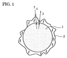
- the particle material for anisotropic conductive connection of the present invention are composed of a conductive particle 1 and an insulating resin layer 2 that covers the surface thereof.
- the insulating resin layer 2 is made up of an insulating gelled resin whose gel proportion is at least 90%, and preferably at least 95%. It is undesirable for the gel proportion to be less than 90% because the insulation characteristics of the anisotropic conductive connection material will deteriorate.
- gel proportion is the gel proportion with respect to the solvent used in the preparation of the anisotropic conductive connection material (at least ethyl acetate, butyl acetate, toluene, n-butanol, methyl isobutyl ketone, xylene, tetrahydrofuran, or methyl ethyl ketone).
- the gel proportion is calculated as follows. 1 g of insulating resin powder is washed centrifugally (50 rpm) for 1 hour in 10 mL of solvent, then centrifugal washing is performed two more times using different solvents, and the weight percentage of the insulating resin after washing with respect to the insulating resin before washing is termed the gel proportion.
- the gel proportion can be adjusted by varying the amount of polyfunctional monomer used in the manufacture of the insulating gelled resin.
- An insulating gelled resin with a gel proportion of at least 90% is used in the present invention, but of these, the use of one whose softening point is higher than the heating temperature during anisotropic conductive connection is preferred. The insulation characteristics will tend to deteriorate if an insulating gelled resin having a softening point lower than the heating temperature during anisotropic conductive connection is used.
- the heating temperature during anisotropic conductive connection will vary with the type of adhesive agent being used and other factors, but is generally between 130 and 200°C.
- the thickness is preferably at least 10 nm but no more than 1/5 the diameter of the conductive particles 1.
- the thickness of the insulating resin layer 2 the following formula (1) is preferably satisfied in order to easily ensure conduction by breaking the insulating layer, if we let t 1 be the maximum thickness of the insulating resin layer and t 2 be the minimum thickness (see Figure 1). 2 ⁇ t 1 /t 2 ⁇ 10
- data for the maximum thickness t 1 and minimum thickness t 2 is preferably obtained by measuring the cross section of the conductive particles for anisotropic conductive connection of the present invention by electron microscopy.
- the coverage of the insulating resin layer 2 on the conductive particle 1 is preferably at least 50%, and even more preferably 60 to 99%, because insulation characteristics will deteriorate if the coverage is too low, but complete coverage will cause distortion to occur due to the difference in the linear coefficients of expansion between the conductive particle 1 and the insulating resin layer 2, and this distortion will produce cracks in the insulating resin layer 2, making it difficult to eliminate the insulating resin layer 2 from the press-bonding surface during press-bonding, increasing the connection resistance, and causing other such problems.
- insulating gelled resins that exhibit the above properties include styrene-divinylbenzene resins and acrylic-styrene resins, but an acrylic-styrene resin is preferable in terms of solvent resistance and heat resistance.
- the same conductive particles for anisotropic conductive connection as those used in the past can be used as the conductive particle 1 covered with the insulating gelled resin.
- solder particles, nickel particles, or other metal particles, composite conductive particles produced by metal-plating the surface of resin particles, or the like can be used.
- the particle material for anisotropic conductive connection of the present invention can be manufactured by fixing the above-mentioned insulating gelled resin powder with a gel proportion of at least 90% to the surface of the conductive particle 1 by a physical/mechanical method to cover the conductive particle 1 with the insulating resin layer 2.
- the term physical/mechanical method as used here refers to a dry method of joining fine powders together. More specifically, while a powder produced by covering a core particle with fine particles which are smaller than the core particle is dispersed in the vapor phase, thermomechanical energy whose main component is impact force is imparted to this powder, and fixing is conducted for a short time (1 to 5 minutes) (T. Kondo and M. Koishi, "Microcapsules, Revised Third Edition," pp.
- the particle material can be manufactured by using a hybridization system made by Nara Kikai Seisakusho (Hybridizer Model 0).
- the specific operating conditions can be suitably determined as dictated by the raw materials and apparatus being used.
- the specific surface area S 1 of the conductive particle and the specific surface area S 2 of the insulating gelled resin powder satisfy the following formula (2): S 2 > 10 ⁇ S 1 and the primary particle diameter R 1 of the conductive particle and the primary particle diameter R 2 of the insulating gelled resin powder satisfy the following formula (3): R 1 > 3 ⁇ R 2
- the softening point thereof, the relation between the layer thickness thereof and the diameter of the conductive particle, the relation between the maximum thickness and the minimum thickness, and the coverage are as described for the particle material for anisotropic conductive connection of the present invention.
- the particle material for anisotropic conductive connection of the present invention as described above can be dispersed in an insulating adhesive agent to manufacture an anisotropic conductive connection material in the form of a paste or film.
- the same adhesive agents as those used in known anisotropic conductive connection materials can be used as this insulating adhesive agent.
- connection structure that exhibits good connection strength, insulation characteristics, and conduction characteristics can be obtained by sandwiching an anisotropic conductive connection material in which the particle material for anisotropic conductive connection of the present invention are used between two opposing connection materials (such as a semiconductor device and its mounting substrate, or a flexible printed substrate and a liquid crystal display), and hot pressing this assembly.
- an anisotropic conductive connection material in which the particle material for anisotropic conductive connection of the present invention are used between two opposing connection materials (such as a semiconductor device and its mounting substrate, or a flexible printed substrate and a liquid crystal display), and hot pressing this assembly.
- Table 1 shows the coverage (%) of the insulating resin layer of the obtained conductive particles, the average thickness ( ⁇ m) of the insulating resin layer, and the ratio (t 1 /t 2 ) between the maximum thickness t 1 and the minimum thickness t 2 of the insulating resin layer.
- Table 2 shows the coverage (%) of the insulating resin layer of the obtained conductive particles, the average thickness ( ⁇ m) of the insulating resin layer, the ratio (t 1 /t 2 ) between the maximum thickness t 1 and the minimum thickness t 2 of the insulating resin layer, and the softening point (°C).
- the particle material for anisotropic conductive connection obtained in the above experimental examples were added and uniformly mixed in an amount of 10 vol% to a mixture composed of 60 weight parts bis A-type solid epoxy resin (Ep 1009, made by Shell Petrochemical), 40 weight parts latent curing agent (Hx3941HP, made by Asahi Chemical), and 70 weight parts toluene.
- This mixture was coated in a dry thickness of 25 ⁇ m with a silicone-treated polyethylene terephthalate film, and this coating was dried to produce an anisotropic conductive connection film.
- the anisotropic conductive connection film thus produced was sandwiched between glass substrates equipped with semiconductor devices at a pitch of 50 ⁇ m (bump size: 35 ⁇ 80 ⁇ m, bump spacing: 15 ⁇ m, bump height: 20 ⁇ m) and ITO at a pitch of 50 ⁇ m (metallization width: 35 ⁇ m, metallization spacing: 15 ⁇ m), and a connection structure was obtained by press bonding for 10 seconds at a temperature of 200°C and a pressure of 3.92 ⁇ 10 7 Pa.
- the connection structure thus obtained was evaluated for conduction characteristics and insulation characteristics as described below. The obtained results are given in Table 3.
- the conductive particles for anisotropic conductive connection of the present invention despite being covered on their surface with an insulating resin, exhibit excellent conduction characteristics and insulation characteristics, and therefore represent an improvement in terms of drawbacks over conventional conductive particles for anisotropic conductive connection covered with a thermoplastic resin or a thermosetting resin.
- a particle material for anisotropic conductive connection is comprised of a conductive particle and an insulating resin layer covering the surface thereof, wherein the insulating resin layer includes an insulating gelled resin with a gel proportion of at least 90%.
- the particle material can be manufactured by fixing an insulating gelled resin powder with a gel proportion of at least 90% to the surface of the conductive particle by a physical/mechanical method to form the insulating resin layer.
Landscapes
- Chemical & Material Sciences (AREA)
- Engineering & Computer Science (AREA)
- Microelectronics & Electronic Packaging (AREA)
- Organic Chemistry (AREA)
- Dispersion Chemistry (AREA)
- Physics & Mathematics (AREA)
- Spectroscopy & Molecular Physics (AREA)
- Manufacturing & Machinery (AREA)
- Health & Medical Sciences (AREA)
- Chemical Kinetics & Catalysis (AREA)
- Medicinal Chemistry (AREA)
- Polymers & Plastics (AREA)
- Non-Insulated Conductors (AREA)
- Conductive Materials (AREA)
- Adhesives Or Adhesive Processes (AREA)
Abstract
Description
| Experimental Example | Coverage (%) | Average film thickness (µm) | Ratio (t1/t2) |
| A1 | 100 | 0.5 | 1.5 |
| A2 | 50 | 0.5 | 1.5 |
| A3 | 40 | 0.5 | 1.5 |
| A4 | 98 | 0.5 | 1.5 |
| A5 | 80 | 0.5 | 1.5 |
| A6 | 100 | 0.5 | 4.5 |
| A7 | 100 | 0.5 | 7.0 |
| A8 | 100 | 0.5 | 11.0 |
| A9 | 80 | 1.5 | 4.5 |
| Experimental example | B1 | B2 | B3 | B4 |
| Degree of crosslinking (%) | 1 | 3 | 5 | 10 |
| Gel proportion (%) | 20 | 70 | 90 | 98 |
| Specific surface area (m2/g) | 21.3 | 20.6 | 23.2 | 22.1 |
| Coverage (%) | 95 | 95 | 95 | 95 |
| Average film thickness (µm) | 0.5 | 0.5 | 0.5 | 0.5 |
| Ratio (t1/t2) | 4.5 | 4.2 | 4.9 | 4.1 |
| Softening point (°C) | 40 | 80 | 100 | 200 |
| Conduction characteristics | |
| Symbol | Evaluation criteria |
| A: | when the initial resistance of all 100 connected pins is 5 Ω or less |
| B: | when the greatest initial resistance among the 100 connected pins is over 5 Ω but less than 10 Ω |
| C: | when the greatest initial resistance among the 100 connected pins is over 10 Ω |
| Insulation characteristics | |
| Symbol | Evaluation criteria |
| A: | when the resistance of 100 disconnected pins is at least 108 Ω |
| B: | when the least resistance of 100 disconnected pins is at least 106 Ω |
| C: | when the least resistance of 100 disconnected pins is less than 106 Ω |
| Experimental example | Conduction characteristics | Insulation characteristics |
| A1 | B | A |
| A2 | A | A |
| A3 | A | B |
| A4 | A | A |
| A5 | A | A |
| A6 | A | A |
| A7 | A | A |
| A8 | A | A |
| A9 | B | A |
| B1 | A | B |
| B2 | A | B |
| B3 | A | B |
| B4 | A | A |
Claims (10)
- A particle material for anisotropic conductive connection, comprising a conductive particle and an insulating resin layer covering the surface thereof, wherein the insulating resin layer comprises an insulating gelled resin with a gel proportion of at least 90%.
- The particle material for anisotropic conductive connection as defined in Claim 1, wherein the insulating gelled resin has a softening point higher than the heating temperature during anisotropic conductive connection.
- The particle material for anisotropic conductive connection as defined in Claim 1 or 2, wherein the thickness of the insulating resin layer is at least 10 nm but no more than 1/5 the diameter of the conductive particles.
- The particle material for anisotropic conductive connection as defined in Claim 1, wherein the following formula (1) is satisfied if t1 is the maximum thickness of the insulating resin layer and t2 is the minimum thickness.
- The particle material for anisotropic conductive connection as defined in Claim 1, wherein the coverage of the insulating resin layer is at least 50%.
- The particle material for anisotropic conductive connection as defined in Claim 1, wherein the insulating gelled resin is an acrylic-styrene resin.
- A method for manufacturing a particle material for anisotropic conductive connection, the particle material comprising a conductive particle and an insulating resin layer covering the surface thereof, wherein the method comprises fixing an insulating gelled resin powder with a gel proportion of at least 90% to the surface of a conductive particle by a physical/mechanical method to form the insulating resin layer.
- The manufacturing method as defined in Claim 7, wherein the specific surface area S1 of the conductive particles and the specific surface area S2 of the insulating gelled resin powder satisfy the following formula (2):
- An anisotropic conductive connection material in which the particle materials for anisotropic conductive connection defined in Claim 1 are dispersed in an insulating adhesive agent.
- A connection structure obtained by connecting two opposing materials to be connected by use of the anisotropic conductive connection material defined in Claim 9.
Applications Claiming Priority (4)
| Application Number | Priority Date | Filing Date | Title |
|---|---|---|---|
| JP31569299 | 1999-11-05 | ||
| JP31569299 | 1999-11-05 | ||
| JP2000178408 | 2000-06-14 | ||
| JP2000178408A JP3346376B2 (en) | 1999-11-05 | 2000-06-14 | Conductive particles for anisotropic conductive connection and anisotropic conductive connection material |
Publications (3)
| Publication Number | Publication Date |
|---|---|
| EP1098361A2 true EP1098361A2 (en) | 2001-05-09 |
| EP1098361A3 EP1098361A3 (en) | 2008-02-27 |
| EP1098361B1 EP1098361B1 (en) | 2019-03-06 |
Family
ID=26568400
Family Applications (1)
| Application Number | Title | Priority Date | Filing Date |
|---|---|---|---|
| EP00123648.8A Expired - Lifetime EP1098361B1 (en) | 1999-11-05 | 2000-10-30 | Particle material, anisotropic conductive connection and anisotropic conductive connection material, method of manufacturing the same, and use of the same |
Country Status (4)
| Country | Link |
|---|---|
| US (1) | US6632532B1 (en) |
| EP (1) | EP1098361B1 (en) |
| JP (1) | JP3346376B2 (en) |
| KR (1) | KR100554925B1 (en) |
Families Citing this family (19)
| Publication number | Priority date | Publication date | Assignee | Title |
|---|---|---|---|---|
| KR100589799B1 (en) | 2003-05-06 | 2006-06-14 | 한화석유화학 주식회사 | Insulated conductive particles for anisotropic conductive connection, manufacturing method thereof and products using the same |
| KR100597391B1 (en) | 2004-05-12 | 2006-07-06 | 제일모직주식회사 | Insulating conductive fine particles and anisotropic conductive adhesive film containing same |
| US8802214B2 (en) | 2005-06-13 | 2014-08-12 | Trillion Science, Inc. | Non-random array anisotropic conductive film (ACF) and manufacturing processes |
| US20060280912A1 (en) * | 2005-06-13 | 2006-12-14 | Rong-Chang Liang | Non-random array anisotropic conductive film (ACF) and manufacturing processes |
| KR100722493B1 (en) | 2005-09-02 | 2007-05-28 | 제일모직주식회사 | Insulating conductive fine particles and anisotropic conductive adhesive film using the same |
| KR100699428B1 (en) * | 2005-09-28 | 2007-03-26 | 전자부품연구원 | Method for producing conductive particles |
| JP4967482B2 (en) * | 2006-02-27 | 2012-07-04 | 日立化成工業株式会社 | Conductive particles, adhesive composition and circuit connecting material |
| US20070246158A1 (en) * | 2006-04-21 | 2007-10-25 | 3M Innovative Properties Company | Wiring board, production process thereof and connection method using same |
| US20100065311A1 (en) | 2006-07-03 | 2010-03-18 | Hitachi Chemical Company, Ltd. | Conductive particle, adhesive composition, circuit-connecting material, circuit-connecting structure, and method for connection of circuit member |
| US7923488B2 (en) * | 2006-10-16 | 2011-04-12 | Trillion Science, Inc. | Epoxy compositions |
| JP5670133B2 (en) * | 2010-09-17 | 2015-02-18 | 株式会社日本触媒 | Resin particles, insulated conductive particles and anisotropic conductive materials using the same |
| JP5134111B2 (en) * | 2011-05-20 | 2013-01-30 | 住友電気工業株式会社 | Connection method, connection structure, and electronic device |
| JP5703149B2 (en) * | 2011-07-06 | 2015-04-15 | 積水化学工業株式会社 | Conductive particles with insulating particles, anisotropic conductive material, and connection structure |
| US9102851B2 (en) | 2011-09-15 | 2015-08-11 | Trillion Science, Inc. | Microcavity carrier belt and method of manufacture |
| US9475963B2 (en) | 2011-09-15 | 2016-10-25 | Trillion Science, Inc. | Fixed array ACFs with multi-tier partially embedded particle morphology and their manufacturing processes |
| KR101403865B1 (en) * | 2011-12-16 | 2014-06-10 | 제일모직주식회사 | Composition for use in an anisotropic conductive film, an anisotropic conductive film and semiconductor device |
| US9352539B2 (en) | 2013-03-12 | 2016-05-31 | Trillion Science, Inc. | Microcavity carrier with image enhancement for laser ablation |
| EP3134769B1 (en) | 2014-04-25 | 2020-08-19 | Hewlett-Packard Development Company, L.P. | Aligned particle layer |
| HK1231568A1 (en) | 2014-04-25 | 2017-12-22 | Hewlett-Packard Development Company, L.P. | Aligned particle coating |
Family Cites Families (17)
| Publication number | Priority date | Publication date | Assignee | Title |
|---|---|---|---|---|
| GB2076843B (en) * | 1980-05-20 | 1983-11-16 | Standard Telephones Cables Ltd | Hydrophobic gel composition |
| US4575432A (en) * | 1984-07-09 | 1986-03-11 | W. R. Grace & Co. | Conductive thermosetting compositions and process for using same |
| JPH0645753B2 (en) * | 1985-02-21 | 1994-06-15 | 三井石油化学工業株式会社 | Polyamide composition |
| US5334330A (en) * | 1990-03-30 | 1994-08-02 | The Whitaker Corporation | Anisotropically electrically conductive composition with thermal dissipation capabilities |
| JPH0512916A (en) * | 1991-06-28 | 1993-01-22 | Toshiba Corp | Conductive particle of anisotropic conductive adhesive |
| JPH07105716A (en) * | 1993-10-05 | 1995-04-21 | Soken Kagaku Kk | Coated particles and anisotropic conductive adhesive |
| JP3364695B2 (en) | 1993-12-28 | 2003-01-08 | ソニーケミカル株式会社 | Circuit connection regeneration method |
| US5851644A (en) * | 1995-08-01 | 1998-12-22 | Loctite (Ireland) Limited | Films and coatings having anisotropic conductive pathways therein |
| US5672297A (en) * | 1995-10-27 | 1997-09-30 | The Dow Chemical Company | Conductive composite articles based on expandable and contractible particulate matrices |
| JP3137578B2 (en) * | 1996-02-27 | 2001-02-26 | ソニーケミカル株式会社 | Conductive particles for anisotropic conductive adhesive film, method for producing the same, and anisotropic conductive adhesive film |
| US5840215A (en) * | 1996-12-16 | 1998-11-24 | Shell Oil Company | Anisotropic conductive adhesive compositions |
| US6833180B1 (en) * | 1997-07-04 | 2004-12-21 | Nippon Zeon Company, Ltd. | Adhesive for semiconductor part |
| JP2836035B2 (en) * | 1997-07-04 | 1998-12-14 | 富士ゼロックス株式会社 | Electrical connection |
| JP3296306B2 (en) | 1997-10-28 | 2002-06-24 | ソニーケミカル株式会社 | Anisotropic conductive adhesive and adhesive film |
| TW459032B (en) * | 1998-03-18 | 2001-10-11 | Sumitomo Bakelite Co | An anisotropic conductive adhesive and method for preparation thereof and an electronic apparatus using said adhesive |
| KR100291662B1 (en) * | 1998-10-15 | 2001-06-01 | 권문구 | Composite powder for anisotropic conductive film |
| EP1228124B1 (en) * | 2000-05-27 | 2004-11-03 | Q-Sys Co., Ltd | Electrically conductive microgel and method for preparing the same |
-
2000
- 2000-06-14 JP JP2000178408A patent/JP3346376B2/en not_active Expired - Lifetime
- 2000-10-23 US US09/693,892 patent/US6632532B1/en not_active Expired - Lifetime
- 2000-10-30 EP EP00123648.8A patent/EP1098361B1/en not_active Expired - Lifetime
- 2000-11-01 KR KR1020000064528A patent/KR100554925B1/en not_active Expired - Lifetime
Also Published As
| Publication number | Publication date |
|---|---|
| EP1098361A3 (en) | 2008-02-27 |
| JP3346376B2 (en) | 2002-11-18 |
| JP2001195921A (en) | 2001-07-19 |
| KR20010060234A (en) | 2001-07-06 |
| US6632532B1 (en) | 2003-10-14 |
| KR100554925B1 (en) | 2006-03-03 |
| EP1098361B1 (en) | 2019-03-06 |
Similar Documents
| Publication | Publication Date | Title |
|---|---|---|
| US6632532B1 (en) | Particle material anisotropic conductive connection and anisotropic conductive connection material | |
| US8846142B2 (en) | Conductive particle, anisotropic conductive interconnection material that uses the conductive particle, and method for producing the conductive particle | |
| TWI386475B (en) | Film, connection method and joint body | |
| US6365840B1 (en) | Electrical connecting device and electrical connecting method | |
| CN112586103B (en) | Electromagnetic wave shielding film, method for manufacturing shielding printed circuit board, and shielding printed circuit board | |
| JP2006525641A (en) | Insulating conductive particles for anisotropic conductive connection, method for producing the same, and products using the same | |
| JP3137578B2 (en) | Conductive particles for anisotropic conductive adhesive film, method for producing the same, and anisotropic conductive adhesive film | |
| JPH06349339A (en) | Anisotropic conductive film | |
| US20020009597A1 (en) | Connecting material and connection structure | |
| KR100845875B1 (en) | Insulation-coated electroconductive particles | |
| JP4110589B2 (en) | Circuit connection member and circuit board manufacturing method | |
| US20020111423A1 (en) | Method for manufacturing conductive adhesive for high frequency flip chip package application | |
| JPH04242010A (en) | Anisotropic conductive agent for connection | |
| JPH09306231A (en) | Conductive particles and substrate | |
| JP2000011760A (en) | Anisotropic conductive composition and method for producing anisotropic conductive member using the same | |
| JP2001308217A (en) | Semiconductor device | |
| JP5143329B2 (en) | Manufacturing method of circuit connection body | |
| JP3480754B2 (en) | Method for producing anisotropic conductive film | |
| KR100313766B1 (en) | Method and conductive powder struture of anisotropic conductive powder | |
| JPH03291807A (en) | Anisotropic conductive paste | |
| JPH08148210A (en) | Connection member | |
| JPH05283480A (en) | How to connect electronic circuit parts | |
| JPH0329209A (en) | Anisotropically conductive film | |
| JP3505321B2 (en) | Conductive fine particles and substrate | |
| KR19980013961A (en) | Anisotropic conductive film |
Legal Events
| Date | Code | Title | Description |
|---|---|---|---|
| PUAI | Public reference made under article 153(3) epc to a published international application that has entered the european phase |
Free format text: ORIGINAL CODE: 0009012 |
|
| AK | Designated contracting states |
Kind code of ref document: A2 Designated state(s): AT BE CH CY DE DK ES FI FR GB GR IE IT LI LU MC NL PT SE |
|
| AX | Request for extension of the european patent |
Free format text: AL;LT;LV;MK;RO;SI |
|
| RAP1 | Party data changed (applicant data changed or rights of an application transferred) |
Owner name: SONY CHEMICAL & INFORMATION DEVICE CORPORATION |
|
| PUAL | Search report despatched |
Free format text: ORIGINAL CODE: 0009013 |
|
| PUAF | Information related to the publication of a search report (a3 document) modified or deleted |
Free format text: ORIGINAL CODE: 0009199SEPU |
|
| PUAL | Search report despatched |
Free format text: ORIGINAL CODE: 0009013 |
|
| AK | Designated contracting states |
Kind code of ref document: A3 Designated state(s): AT BE CH CY DE DK ES FI FR GB GR IE IT LI LU MC NL PT SE |
|
| AX | Request for extension of the european patent |
Extension state: AL LT LV MK RO SI |
|
| D17D | Deferred search report published (deleted) | ||
| AK | Designated contracting states |
Kind code of ref document: A3 Designated state(s): AT BE CH CY DE DK ES FI FR GB GR IE IT LI LU MC NL PT SE |
|
| AX | Request for extension of the european patent |
Extension state: AL LT LV MK RO SI |
|
| 17P | Request for examination filed |
Effective date: 20080610 |
|
| AKX | Designation fees paid |
Designated state(s): DE FR GB |
|
| 17Q | First examination report despatched |
Effective date: 20081112 |
|
| RAP1 | Party data changed (applicant data changed or rights of an application transferred) |
Owner name: DEXERIALS CORPORATION |
|
| REG | Reference to a national code |
Ref country code: DE Ref legal event code: R079 Ref document number: 60049903 Country of ref document: DE Free format text: PREVIOUS MAIN CLASS: H01L0021600000 Ipc: H01B0001220000 |
|
| GRAP | Despatch of communication of intention to grant a patent |
Free format text: ORIGINAL CODE: EPIDOSNIGR1 |
|
| RIC1 | Information provided on ipc code assigned before grant |
Ipc: H05K 3/32 19680901ALI20180831BHEP Ipc: H01L 21/60 19740701ALI20180831BHEP Ipc: C09J 9/02 19900101ALN20180831BHEP Ipc: H01B 1/22 19800101AFI20180831BHEP Ipc: H01R 4/04 19800101ALI20180831BHEP Ipc: H01R 13/03 19850101ALI20180831BHEP |
|
| INTG | Intention to grant announced |
Effective date: 20181005 |
|
| RIC1 | Information provided on ipc code assigned before grant |
Ipc: H01R 13/03 19850101ALI20180926BHEP Ipc: H01L 21/60 19740701ALI20180926BHEP Ipc: H01B 1/22 19800101AFI20180926BHEP Ipc: H05K 3/32 19680901ALI20180926BHEP Ipc: H01R 4/04 19800101ALI20180926BHEP Ipc: C09J 9/02 19900101ALN20180926BHEP |
|
| GRAS | Grant fee paid |
Free format text: ORIGINAL CODE: EPIDOSNIGR3 |
|
| GRAA | (expected) grant |
Free format text: ORIGINAL CODE: 0009210 |
|
| RIC1 | Information provided on ipc code assigned before grant |
Ipc: H01L 21/60 20060101ALI20180926BHEP Ipc: H05K 3/32 20060101ALI20180926BHEP Ipc: C09J 9/02 20060101ALN20180926BHEP Ipc: H01R 4/04 20060101ALI20180926BHEP Ipc: H01R 13/03 20060101ALI20180926BHEP Ipc: H01B 1/22 20060101AFI20180926BHEP |
|
| AK | Designated contracting states |
Kind code of ref document: B1 Designated state(s): DE FR GB |
|
| REG | Reference to a national code |
Ref country code: GB Ref legal event code: FG4D |
|
| REG | Reference to a national code |
Ref country code: DE Ref legal event code: R096 Ref document number: 60049903 Country of ref document: DE |
|
| PGFP | Annual fee paid to national office [announced via postgrant information from national office to epo] |
Ref country code: FR Payment date: 20190913 Year of fee payment: 20 |
|
| REG | Reference to a national code |
Ref country code: DE Ref legal event code: R097 Ref document number: 60049903 Country of ref document: DE |
|
| PLBE | No opposition filed within time limit |
Free format text: ORIGINAL CODE: 0009261 |
|
| STAA | Information on the status of an ep patent application or granted ep patent |
Free format text: STATUS: NO OPPOSITION FILED WITHIN TIME LIMIT |
|
| PGFP | Annual fee paid to national office [announced via postgrant information from national office to epo] |
Ref country code: DE Payment date: 20191015 Year of fee payment: 20 |
|
| 26N | No opposition filed |
Effective date: 20191209 |
|
| PGFP | Annual fee paid to national office [announced via postgrant information from national office to epo] |
Ref country code: GB Payment date: 20191031 Year of fee payment: 20 |
|
| REG | Reference to a national code |
Ref country code: DE Ref legal event code: R071 Ref document number: 60049903 Country of ref document: DE |
|
| REG | Reference to a national code |
Ref country code: GB Ref legal event code: PE20 Expiry date: 20201029 |
|
| PG25 | Lapsed in a contracting state [announced via postgrant information from national office to epo] |
Ref country code: GB Free format text: LAPSE BECAUSE OF EXPIRATION OF PROTECTION Effective date: 20201029 |