EP1091255A2 - Procédé pour aligner un masque et un substrat dans un appareil d'exposition - Google Patents
Procédé pour aligner un masque et un substrat dans un appareil d'exposition Download PDFInfo
- Publication number
- EP1091255A2 EP1091255A2 EP00121522A EP00121522A EP1091255A2 EP 1091255 A2 EP1091255 A2 EP 1091255A2 EP 00121522 A EP00121522 A EP 00121522A EP 00121522 A EP00121522 A EP 00121522A EP 1091255 A2 EP1091255 A2 EP 1091255A2
- Authority
- EP
- European Patent Office
- Prior art keywords
- workpiece
- marks
- mask
- spatial coordinates
- mark
- Prior art date
- Legal status (The legal status is an assumption and is not a legal conclusion. Google has not performed a legal analysis and makes no representation as to the accuracy of the status listed.)
- Withdrawn
Links
Images


Classifications
-
- G—PHYSICS
- G03—PHOTOGRAPHY; CINEMATOGRAPHY; ANALOGOUS TECHNIQUES USING WAVES OTHER THAN OPTICAL WAVES; ELECTROGRAPHY; HOLOGRAPHY
- G03F—PHOTOMECHANICAL PRODUCTION OF TEXTURED OR PATTERNED SURFACES, e.g. FOR PRINTING, FOR PROCESSING OF SEMICONDUCTOR DEVICES; MATERIALS THEREFOR; ORIGINALS THEREFOR; APPARATUS SPECIALLY ADAPTED THEREFOR
- G03F9/00—Registration or positioning of originals, masks, frames, photographic sheets or textured or patterned surfaces, e.g. automatically
- G03F9/70—Registration or positioning of originals, masks, frames, photographic sheets or textured or patterned surfaces, e.g. automatically for microlithography
- G03F9/7088—Alignment mark detection, e.g. TTR, TTL, off-axis detection, array detector, video detection
-
- H—ELECTRICITY
- H01—ELECTRIC ELEMENTS
- H01L—SEMICONDUCTOR DEVICES NOT COVERED BY CLASS H10
- H01L21/00—Processes or apparatus adapted for the manufacture or treatment of semiconductor or solid state devices or of parts thereof
- H01L21/02—Manufacture or treatment of semiconductor devices or of parts thereof
- H01L21/027—Making masks on semiconductor bodies for further photolithographic processing not provided for in group H01L21/18 or H01L21/34
-
- G—PHYSICS
- G03—PHOTOGRAPHY; CINEMATOGRAPHY; ANALOGOUS TECHNIQUES USING WAVES OTHER THAN OPTICAL WAVES; ELECTROGRAPHY; HOLOGRAPHY
- G03F—PHOTOMECHANICAL PRODUCTION OF TEXTURED OR PATTERNED SURFACES, e.g. FOR PRINTING, FOR PROCESSING OF SEMICONDUCTOR DEVICES; MATERIALS THEREFOR; ORIGINALS THEREFOR; APPARATUS SPECIALLY ADAPTED THEREFOR
- G03F9/00—Registration or positioning of originals, masks, frames, photographic sheets or textured or patterned surfaces, e.g. automatically
- G03F9/70—Registration or positioning of originals, masks, frames, photographic sheets or textured or patterned surfaces, e.g. automatically for microlithography
- G03F9/7073—Alignment marks and their environment
- G03F9/7076—Mark details, e.g. phase grating mark, temporary mark
-
- G—PHYSICS
- G03—PHOTOGRAPHY; CINEMATOGRAPHY; ANALOGOUS TECHNIQUES USING WAVES OTHER THAN OPTICAL WAVES; ELECTROGRAPHY; HOLOGRAPHY
- G03F—PHOTOMECHANICAL PRODUCTION OF TEXTURED OR PATTERNED SURFACES, e.g. FOR PRINTING, FOR PROCESSING OF SEMICONDUCTOR DEVICES; MATERIALS THEREFOR; ORIGINALS THEREFOR; APPARATUS SPECIALLY ADAPTED THEREFOR
- G03F9/00—Registration or positioning of originals, masks, frames, photographic sheets or textured or patterned surfaces, e.g. automatically
- G03F9/70—Registration or positioning of originals, masks, frames, photographic sheets or textured or patterned surfaces, e.g. automatically for microlithography
- G03F9/7092—Signal processing
-
- H—ELECTRICITY
- H05—ELECTRIC TECHNIQUES NOT OTHERWISE PROVIDED FOR
- H05K—PRINTED CIRCUITS; CASINGS OR CONSTRUCTIONAL DETAILS OF ELECTRIC APPARATUS; MANUFACTURE OF ASSEMBLAGES OF ELECTRICAL COMPONENTS
- H05K3/00—Apparatus or processes for manufacturing printed circuits
- H05K3/0008—Apparatus or processes for manufacturing printed circuits for aligning or positioning of tools relative to the circuit board
-
- H—ELECTRICITY
- H05—ELECTRIC TECHNIQUES NOT OTHERWISE PROVIDED FOR
- H05K—PRINTED CIRCUITS; CASINGS OR CONSTRUCTIONAL DETAILS OF ELECTRIC APPARATUS; MANUFACTURE OF ASSEMBLAGES OF ELECTRICAL COMPONENTS
- H05K3/00—Apparatus or processes for manufacturing printed circuits
- H05K3/0073—Masks not provided for in groups H05K3/02 - H05K3/46, e.g. for photomechanical production of patterned surfaces
- H05K3/0082—Masks not provided for in groups H05K3/02 - H05K3/46, e.g. for photomechanical production of patterned surfaces characterised by the exposure method of radiation-sensitive masks
Definitions
- the present invention concerns a method of aligning a mask and workpiece in which the spatial coordinates of mask alignment marks (hereinafter abbreviated mask marks) formed on a mask and of workpiece alignment marks (hereinafter abbreviated workpiece marks) formed on a workpiece are detected by image processing in an exposure device, after which the mask and workpiece are aligned based on the detected spatial coordinates.
- mask marks mask alignment marks
- workpiece marks workpiece alignment marks
- Exposure devices are used in the process of manufacturing patterns in semiconductor devices, printed circuit boards, liquid-crystal boards, etc., by photolithography. Such an exposure device exposes (transfers) a mask pattern to a workpiece after the mask on which a mask pattern has been formed is aligned with the workpiece and light, including exposure light, is irradiated via the mask.
- Examples of exposure devices include a projection exposure device which focuses a mask image on a workpiece via a projection lens, etc., and then exposes a mask pattern on a workpiece, a proximity exposure device which irradiates parallel light on a mask while a slight gap is established between a mask and workpiece and then exposes a mask pattern on a workpiece, and a contact exposure device which irradiates parallel light on a mask while a mask and workpiece are in contact and then exposes a mask pattern on a workpiece.
- a projection exposure device which focuses a mask image on a workpiece via a projection lens, etc., and then exposes a mask pattern on a workpiece
- a proximity exposure device which irradiates parallel light on a mask while a slight gap is established between a mask and workpiece and then exposes a mask pattern on a workpiece
- a contact exposure device which irradiates parallel light on a mask while a mask and workpiece are in contact and then exposes a
- a mask and workpiece are aligned in the aforementioned exposure device as follows.
- Mask marks formed on a mask and workpiece marks formed on a workpiece are detected by an alignment microscope.
- the detection data are subjected to image processing, their spatial coordinates are determined, and the mask or workpiece is moved so that their positions will have a preset spatial relationship.
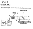
- Figure 8 is a diagrammatic view of alignment microscope 10 which detects workpiece marks. Detection of workpiece marks in a proximity exposure device or a contact exposure device as well as the detection of mask marks are carried out in the same manner.
- Alignment microscope 10 in Figure 8 comprises a half mirror 10a, lenses L1, L2 and a CCD camera 10b.
- a processing unit 11 carries out image processing, and is connected to a monitor 12.
- W denotes a workpiece on which workpiece mark WAM is formed which is detected by conducting of a pattern search as follows:
- Workpiece mark WAM is registered on processing unit 11.
- a cruciform mark as shown in Figure 9(a), for example, is used as workpiece mark WAM, and a pattern of workpiece marks in which monitor pixels as the discrete units as shown in Figure 9(b) is registered in processing unit 11.
- the number of pixels is set at 5 x 5 in said diagram to facilitate the explanation.
- the registration of aforementioned workpiece mark is explained concretely below.
- the registered workpiece mark WAM is detected by alignment microscope 10 (for example, 3-power magnification).
- the range at which image processing by processing unit 11 is possible (for example, 15 mm x 15 mm range as shown in Figure 10) is then displayed on monitor 12 following reception by alignment microscope 10.
- workpiece mark WAM is enclosed by virtual lines (dotted lines in Figure 10) for workpiece mark registration so as to contain the entire registered workpiece mark WAM.
- Workpiece mark WAM is then registered in processing unit 11.
- Processing unit 11 records workpiece mark WAM via the contrast, taking pixels enclosed by aforementioned virtual lines as discrete units. With that, the workpiece mark WAM registration operation is completed.
- the size of the workpiece mark varies with the type of workpiece, the user, and the procedures. For example, the size of the virtual lines enclosing workpiece mark WAM would frequently be 200 ⁇ m to 700 ⁇ m, as shown in Figure 10.
- the shape of the workpiece mark WAM would frequently vary for the same reasons as those noted above. It is not restricted to the cruciform shape shown in Figure 9.
- the circle shown in Figure 11(a) or the irregular pattern shown in Figure 11(b) that comprises a set may serve as alignment marks. In any event, the registration range is set so as to include all patterns of a workpiece mark.
- Workpiece mark WAM on workpiece W is irradiated with illuminating light via half mirror 10a of alignment unit 10, as shown in Figure 8, and workpiece mark WAM is imaged by CCD camera 10b.
- the image of workpiece mark WAM shown in monitor 12 is input to processing unit 11 and is converted into coordinate data using pixels of monitor 12 as discrete units.
- Processing unit 11 compares the aforementioned registered pattern with the image of imaged workpiece mark WAM. For example, the score (correlated value) would be perceived as 60 if the image of the imaged workpiece mark WAM (detected pattern) coincides with 60% of the registered pattern in the case of the detected pattern A shown in Figure 9(c).
- the score would be perceived as 80 if the image of the imaged workpiece mark WAM (detected pattern) coincides with 80% of the registered pattern in the case of the detected pattern B shown in Figure 9(d). Furthermore, the score would be perceived as 100 if the image of the imaged workpiece mark WAM (detected pattern) coincides with 100% of the registered pattern in the case of the detected pattern C shown in Figure 9(e). As shown above, the entire range shown on the monitor is subjected to a pattern search, and each detected pattern whose score approaches 100 (the highest) is perceived as workpiece mark WAM. Its spatial coordinates are recorded as the spatial coordinates of the workpiece mark.
- the alignment accuracy is reduced by the following factors in aligning aforementioned marks and workpiece:
- a first object is to provide a method of aligning a mask and workpiece in an exposure device which permits the mask and workpiece to be aligned accurately while minimizing the reduction in alignment accuracy of the mask and workpiece should the shape of the alignment marks be deformed or the position relative to set values be shifted.
- a second object is to permit alignment in which the required alignment accuracy is ensured by aligning a mask and workpiece after selecting only those alignment marks having high reliability by verifying the reliability of the spatial coordinates of the alignment marks.
- Figure 1 shows the structure of a projection exposure device which is applicable to attainment of the objects of the present invention.
- This projection exposure device comprises a mask stage MS, upon which is laid at least one mask mark MAM, and a mask M upon which a mask pattern is formed.
- Exposure light is emitted from an optical irradiation device 1 and is irradiated upon a workpiece W laid on a workpiece stage WS through mask M and a projection lens 2.
- the mask pattern formed on mask M is projected onto workpiece W and the mask pattern upon the workpiece W is thereby exposed.
- An alignment microscope 10 can move in the directions indicated by the arrows in the diagram and is mounted at each of two sites between projection lens 2 and workpiece W (only one alignment microscope being shown in Figure 1). Alignment microscope 10 is inserted at the position shown in the diagram before the mask pattern formed on mask M is exposed on workpiece W, and mask M is aligned with workpiece W.
- alignment microscope 10 comprises a half mirror 10a, lens L1, L2 and CCD camera 10b.
- L (x1y2-x1y3+x2y3-x2y1+x3y1-x3y2) ⁇ 2
- the spatial coordinates (o1x, o1y) of center 01 determined by above computations is the average of the spatial coordinates of three workpiece marks similarly to the coordinate position which was averaged as explained above.
- a different combination of three workpiece marks can be selected and the center 02 of a circle which circumscribes a triangle formed by this combination of three marks can be determined similarly to the manner discussed above, and likewise the centers of circles which circumscribe third and fourth triangles of differing combinations of three workpiece marks can be calculated in the same manner.
- the alignment accuracy could be enhanced further as in the first case above by further averaging of these spatial coordinates since the positions of aforementioned 01, 02 ... would match.
- the averages of the spatial coordinates of the workpiece marks remaining after excluding those with low scores from among the workpiece marks which were detected may be determined in this working example as well.
- the alignment accuracy can be enhanced further by so doing.
- the following advantages are realized just as in the first example by determining the average workpiece mark spatial coordinates using a plurality of workpiece marks as mentioned above. For example, when one of the eight workpiece marks in Figure 3 deviates from the field (search range) of the alignment microscope because of problems involving the spatial accuracy which was set or when the workpiece mark peels from the workpiece because of excessive process defects, the average workpiece mark spatial coordinates can be determined using the remaining workpiece marks which can be utilized.
- this embodiment can accommodate flexibility if any workpiece marks are lost or if part of a group of workpiece marks should fall outside of the field of the alignment microscope since a plurality of coordinates of the center of a circumscribed circle can be determined by altering the combination of three workpiece marks.
- process evaluation of the preceding procedures can be carried out as follows in addition to reducing exacerbation of the alignment accuracy.
- the distance between workpiece marks is known from the set values.
- the spatial coordinates of workpiece marks which are actually affixed can be determined, the distance between them can be calculated, Accordingly, anomalies in distances between workpiece marks can be detected by comparing the distance between workpiece marks which were affixed on each workpiece and the set values. Any process deficiencies in the preceding procedure which lead to anomalies in the workpiece mark position can be detected and the production process of the preceding procedure can be revised. The production of rejects in later procedures can be prevented as a result.
- workpiece marks which allow the required alignment accuracy to be ensured can be selected as follows.
- the position of the workpiece marks is assumed to be dispersed with a regular distribution relative to the original position (set position). Assuming the standard deviation to be ⁇ 1 when they have an ideal regular distribution as shown in Figure 4(a), each datum would lie within the range of ⁇ 3 ⁇ 1 at a probability above 99%. Specifically, even if the spatial coordinates of a workpiece mark should deviate from the original position, there is a probability above 99% that the maximum value of that deviation would be within 3 ⁇ 1 (here, 3 ⁇ 1 denotes the workpiece mark accuracy).
- the alignment accuracy is enhanced by alignment to the average workpiece mark spatial coordinates obtained by aforementioned averaging.
- any two pieces of data would be picked from N number of data groups (for example, the data group shown in Figure 4(a)) having standard deviation of ⁇ 1 and averaged.
- the distribution would be narrower than Figure 4(a) as shown in Figure 4(b) assuming a new data group to be constructed from the data determined following averaging.
- the standard deviation would be ⁇ 2 ⁇ 0.7 ⁇ 1.
- Figure 5 is a diagram showing one example of the relation between the number of averaged workpiece marks and the averaging effect.
- the abscissa represents the number of workpiece marks while the ordinate represents the value obtained after dividing the standard deviation ⁇ n of the data group which averaged n number of workpiece marks by ⁇ 1, the standard deviation of the original data group, that is, ⁇ n/ ⁇ 1.
- Figure 5 itself presents a calculation of the averaging effect using a suitably generated random number table as the original data group.
- the standard deviation ⁇ 2 of the averages of the spatial coordinates of two workpiece marks would be about 0.7 ⁇ 1 due to aforementioned averaging effect.
- the standard deviation ⁇ 3 would be appropriately 0.6 ⁇ 1 if the spatial coordinates of three workpiece marks are averaged.
- the number of averaged workpiece marks can be determined as follows.
- the amount of deviation between the distance between the spatial coordinates of each workpiece mark which was detected and the average workpiece marks versus the distance between the spatial coordinates of the original workpiece marks and the average spatial coordinates is computed. Any spatial coordinates of workpiece marks in which the amount of deviation exceeds a given level are dropped from averaging. By so doing, obstruction of the averaging effect due to mistaken recognition of dirt, for example, adhering to a workpiece as a workpiece mark can be prevented. Depending on the extent of aforementioned deviation, the question of whether or not samples are excluded from averaging would be suitably set in light of the variations in the samples of workpiece marks which were created.
- the pattern of a workpiece mark under a mask mark should appear when observing mask marks in proximity exposure devices and contact exposure devices using an alignment microscope, it is detected by a shape which appears as if the mask mark were deformed although the two are overlaid, and aforementioned detection accuracy (reliability) of the mask mark would fall.
- MS represents the mask stage upon which are laid mask marks MAM and mask M on which is formed a mask pattern.
- WS represents the workpiece stage upon which is laid a workpiece on which is formed workpiece mark WAM.
- Exposure light is emitted from optical irradiation device 1 and is irradiated on the workpiece W on workpiece stage WS through mask M.
- the mask pattern that is formed on mask M is then projected onto workpiece W and a mask pattern is thus exposed on workpiece W.
- Alignment microscope 10 that can move in the direction of the arrows in the diagram is mounted over mask M and alignment microscope 10 is inserted at the position shown in the diagram before the mask pattern formed on mask M is exposed on workpiece W. Mask M is then aligned with workpiece W.
- Alignment microscope 10 is comprised of a half mirror, lens and CCD camera, etc., as shown in aforementioned Figure 8.
- the mask mark image and the pattern of workpiece marks WAM, etc., on workpiece W are both imaged by alignment microscope 10 when mask M is brought into proximity of workpiece W. Accordingly, the shape of the mask mark MAM may appear to change depending on the surface state of workpiece W. This can lower the detection accuracy of mask mark MAM as well as the alignment accuracy.
- mask marks MAM1 - MAM4 are arranged so as to enter one field of the alignment microscope as shown in Figure 7.
- the score of detected mask marks MAM1 to MAM4 is determined as indicated above, and alignment is carried out using the mask marks which remain after eliminating those with a low score.
- a plurality of workpiece marks WAM are affixed on workpiece W corresponding to mask marks MAM 1-4.
- Mask M and workpiece M may be aligned so that the average spatial coordinates of both would coincide, or one workpiece mark WAM could be affixed on the workpiece W and the positions of a plurality of mask marks MAM 1-4 may be averaged.
- the mask mark average spatial coordinates which would form the baseline for alignment, the aforementioned workpiece mark WAM could be determined and mask M could be aligned with workpiece W so that said mask mark average spatial coordinates coincide with the workpiece mark WAM.
- Via holes are created by processing using laser light, for example.
- the diameter of via holes is usually 150 to 200 ⁇ m.
- the processing spatial accuracy using laser processing is about ⁇ 20 ⁇ m at present. In that range, the position of workpiece marks (via holes in this case) varies.
- a plurality of via holes are created as workpiece marks.
- the average spatial coordinates are determined from the spatial coordinates of a plurality of via holes as mentioned above, and the printed circuit board is aligned using such average spatial coordinates as the baseline. Decline in the alignment accuracy due to variation in the processing spatial accuracy of via holes can be avoided by so doing.
Landscapes
- General Physics & Mathematics (AREA)
- Engineering & Computer Science (AREA)
- Physics & Mathematics (AREA)
- Manufacturing & Machinery (AREA)
- Signal Processing (AREA)
- Condensed Matter Physics & Semiconductors (AREA)
- Multimedia (AREA)
- Computer Hardware Design (AREA)
- Microelectronics & Electronic Packaging (AREA)
- Power Engineering (AREA)
- Exposure And Positioning Against Photoresist Photosensitive Materials (AREA)
- Exposure Of Semiconductors, Excluding Electron Or Ion Beam Exposure (AREA)
- Image Analysis (AREA)
Applications Claiming Priority (2)
| Application Number | Priority Date | Filing Date | Title |
|---|---|---|---|
| JP28250699A JP2001110697A (ja) | 1999-10-04 | 1999-10-04 | 露光装置におけるマスクとワークの位置合わせ方法 |
| JP28250699 | 1999-10-04 |
Publications (1)
| Publication Number | Publication Date |
|---|---|
| EP1091255A2 true EP1091255A2 (fr) | 2001-04-11 |
Family
ID=17653338
Family Applications (1)
| Application Number | Title | Priority Date | Filing Date |
|---|---|---|---|
| EP00121522A Withdrawn EP1091255A2 (fr) | 1999-10-04 | 2000-09-30 | Procédé pour aligner un masque et un substrat dans un appareil d'exposition |
Country Status (4)
| Country | Link |
|---|---|
| EP (1) | EP1091255A2 (fr) |
| JP (1) | JP2001110697A (fr) |
| KR (1) | KR20010039990A (fr) |
| TW (1) | TW460920B (fr) |
Cited By (4)
| Publication number | Priority date | Publication date | Assignee | Title |
|---|---|---|---|---|
| CN102566338A (zh) * | 2010-12-28 | 2012-07-11 | 上海微电子装备有限公司 | 光刻对准系统中对对准位置进行修正的方法 |
| US8576374B2 (en) | 2008-03-12 | 2013-11-05 | Asml Netherlands B.V. | Lithographic apparatus and method |
| DE102005025474B4 (de) * | 2004-06-03 | 2017-06-22 | Via Mechanics, Ltd. | Verfahren zur Bestimmung einer Position eines Bezugspunktes |
| CN113791588A (zh) * | 2021-08-11 | 2021-12-14 | 宁波帅特龙集团有限公司 | 一种产线监测系统及其控制方法 |
Families Citing this family (5)
| Publication number | Priority date | Publication date | Assignee | Title |
|---|---|---|---|---|
| JP5298792B2 (ja) * | 2008-11-14 | 2013-09-25 | ウシオ電機株式会社 | アライメントマークの検出方法 |
| JP6401501B2 (ja) * | 2014-06-02 | 2018-10-10 | キヤノン株式会社 | インプリント装置、および物品の製造方法 |
| JP6714477B2 (ja) | 2016-09-09 | 2020-06-24 | 株式会社アドテックエンジニアリング | 基板角位置特定方法 |
| CN112087887B (zh) * | 2019-06-12 | 2023-06-09 | 奥特斯科技(重庆)有限公司 | 通过组合评估垫型和孔型对准标记来对准部件承载件结构 |
| JP7310472B2 (ja) * | 2019-09-13 | 2023-07-19 | 信越化学工業株式会社 | 反射型マスクブランクの製造方法 |
-
1999
- 1999-10-04 JP JP28250699A patent/JP2001110697A/ja active Pending
-
2000
- 2000-08-29 TW TW089117527A patent/TW460920B/zh not_active IP Right Cessation
- 2000-09-30 EP EP00121522A patent/EP1091255A2/fr not_active Withdrawn
- 2000-10-04 KR KR1020000058180A patent/KR20010039990A/ko not_active Application Discontinuation
Cited By (4)
| Publication number | Priority date | Publication date | Assignee | Title |
|---|---|---|---|---|
| DE102005025474B4 (de) * | 2004-06-03 | 2017-06-22 | Via Mechanics, Ltd. | Verfahren zur Bestimmung einer Position eines Bezugspunktes |
| US8576374B2 (en) | 2008-03-12 | 2013-11-05 | Asml Netherlands B.V. | Lithographic apparatus and method |
| CN102566338A (zh) * | 2010-12-28 | 2012-07-11 | 上海微电子装备有限公司 | 光刻对准系统中对对准位置进行修正的方法 |
| CN113791588A (zh) * | 2021-08-11 | 2021-12-14 | 宁波帅特龙集团有限公司 | 一种产线监测系统及其控制方法 |
Also Published As
| Publication number | Publication date |
|---|---|
| KR20010039990A (ko) | 2001-05-15 |
| JP2001110697A (ja) | 2001-04-20 |
| TW460920B (en) | 2001-10-21 |
Similar Documents
| Publication | Publication Date | Title |
|---|---|---|
| US7590280B2 (en) | Position detection apparatus and exposure apparatus | |
| US7466414B2 (en) | Position detection apparatus and method | |
| US20050271954A1 (en) | Alignment mark, alignment apparatus and method, exposure apparatus, and device manufacturing method | |
| JP4946668B2 (ja) | 基板位置検出装置及び基板位置検出方法 | |
| US20110075123A1 (en) | Method for detecting work alignment mark and exposure apparatus using the same | |
| US7339663B2 (en) | Method and apparatus for classifying repetitive defects on a substrate | |
| JP5298792B2 (ja) | アライメントマークの検出方法 | |
| EP1091255A2 (fr) | Procédé pour aligner un masque et un substrat dans un appareil d'exposition | |
| US6600561B2 (en) | Apparatus and method for measuring pattern alignment error | |
| JP5414921B2 (ja) | 検出装置及び方法、露光装置、デバイス製造方法 | |
| JPH08181053A (ja) | 位置検出方法 | |
| JP2000137003A (ja) | パターン検査方法及びその装置 | |
| JPH104044A (ja) | パターン検出方法ならびにアライメントマーク検出方法およびそれを用いた光学装置 | |
| JPH0443407B2 (fr) | ||
| JP3381225B2 (ja) | 位置決め方法及び位置決め装置 | |
| JPH04166710A (ja) | 表面性状観測装置 | |
| JPH06204308A (ja) | 半導体ウエハの特殊パターン位置認識方法 | |
| JPH11239952A (ja) | アライメント検出装置 | |
| JPH10186634A (ja) | フォトマスク | |
| JPH07175522A (ja) | 位置合せ装置と位置合せ方法及びベアボ−ドテスタ | |
| JPH10105720A (ja) | 孔位置の光学的計測方法 | |
| JPH0799732B2 (ja) | 位置合わせ方法 | |
| JPH0571166B2 (fr) | ||
| JPS60246645A (ja) | 半導体ウエハチツプの位置合わせ方法 | |
| JPS61271833A (ja) | 位置検出装置 |
Legal Events
| Date | Code | Title | Description |
|---|---|---|---|
| PUAI | Public reference made under article 153(3) epc to a published international application that has entered the european phase |
Free format text: ORIGINAL CODE: 0009012 |
|
| AK | Designated contracting states |
Kind code of ref document: A2 Designated state(s): AT BE CH CY DE DK ES FI FR GB GR IE IT LI LU MC NL PT SE |
|
| AX | Request for extension of the european patent |
Free format text: AL;LT;LV;MK;RO;SI |
|
| STAA | Information on the status of an ep patent application or granted ep patent |
Free format text: STATUS: THE APPLICATION IS DEEMED TO BE WITHDRAWN |
|
| 18D | Application deemed to be withdrawn |
Effective date: 20040401 |