EP1087652B1 - Verbesserungen für gekühlte elektronische Baugruppen, insbesondere für Steuerungsmodul eines Kraftfahrzeugscheinwerfers - Google Patents
Verbesserungen für gekühlte elektronische Baugruppen, insbesondere für Steuerungsmodul eines Kraftfahrzeugscheinwerfers Download PDFInfo
- Publication number
- EP1087652B1 EP1087652B1 EP00402504A EP00402504A EP1087652B1 EP 1087652 B1 EP1087652 B1 EP 1087652B1 EP 00402504 A EP00402504 A EP 00402504A EP 00402504 A EP00402504 A EP 00402504A EP 1087652 B1 EP1087652 B1 EP 1087652B1
- Authority
- EP
- European Patent Office
- Prior art keywords
- printed circuit
- base plate
- circuit card
- assembly according
- layer
- Prior art date
- Legal status (The legal status is an assumption and is not a legal conclusion. Google has not performed a legal analysis and makes no representation as to the accuracy of the status listed.)
- Expired - Lifetime
Links
Images



Classifications
-
- H—ELECTRICITY
- H05—ELECTRIC TECHNIQUES NOT OTHERWISE PROVIDED FOR
- H05K—PRINTED CIRCUITS; CASINGS OR CONSTRUCTIONAL DETAILS OF ELECTRIC APPARATUS; MANUFACTURE OF ASSEMBLAGES OF ELECTRICAL COMPONENTS
- H05K7/00—Constructional details common to different types of electric apparatus
- H05K7/20—Modifications to facilitate cooling, ventilating, or heating
- H05K7/2039—Modifications to facilitate cooling, ventilating, or heating characterised by the heat transfer by conduction from the heat generating element to a dissipating body
- H05K7/20436—Inner thermal coupling elements in heat dissipating housings, e.g. protrusions or depressions integrally formed in the housing
- H05K7/2049—Pressing means used to urge contact, e.g. springs
-
- H—ELECTRICITY
- H05—ELECTRIC TECHNIQUES NOT OTHERWISE PROVIDED FOR
- H05K—PRINTED CIRCUITS; CASINGS OR CONSTRUCTIONAL DETAILS OF ELECTRIC APPARATUS; MANUFACTURE OF ASSEMBLAGES OF ELECTRICAL COMPONENTS
- H05K3/00—Apparatus or processes for manufacturing printed circuits
- H05K3/0058—Laminating printed circuit boards onto other substrates, e.g. metallic substrates
- H05K3/0061—Laminating printed circuit boards onto other substrates, e.g. metallic substrates onto a metallic substrate, e.g. a heat sink
-
- H—ELECTRICITY
- H05—ELECTRIC TECHNIQUES NOT OTHERWISE PROVIDED FOR
- H05K—PRINTED CIRCUITS; CASINGS OR CONSTRUCTIONAL DETAILS OF ELECTRIC APPARATUS; MANUFACTURE OF ASSEMBLAGES OF ELECTRICAL COMPONENTS
- H05K1/00—Printed circuits
- H05K1/02—Details
- H05K1/0201—Thermal arrangements, e.g. for cooling, heating or preventing overheating
- H05K1/0203—Cooling of mounted components
- H05K1/0204—Cooling of mounted components using means for thermal conduction connection in the thickness direction of the substrate
- H05K1/0206—Cooling of mounted components using means for thermal conduction connection in the thickness direction of the substrate by printed thermal vias
-
- H—ELECTRICITY
- H05—ELECTRIC TECHNIQUES NOT OTHERWISE PROVIDED FOR
- H05K—PRINTED CIRCUITS; CASINGS OR CONSTRUCTIONAL DETAILS OF ELECTRIC APPARATUS; MANUFACTURE OF ASSEMBLAGES OF ELECTRICAL COMPONENTS
- H05K2201/00—Indexing scheme relating to printed circuits covered by H05K1/00
- H05K2201/02—Fillers; Particles; Fibers; Reinforcement materials
- H05K2201/0203—Fillers and particles
- H05K2201/0206—Materials
- H05K2201/0209—Inorganic, non-metallic particles
-
- H—ELECTRICITY
- H05—ELECTRIC TECHNIQUES NOT OTHERWISE PROVIDED FOR
- H05K—PRINTED CIRCUITS; CASINGS OR CONSTRUCTIONAL DETAILS OF ELECTRIC APPARATUS; MANUFACTURE OF ASSEMBLAGES OF ELECTRICAL COMPONENTS
- H05K2201/00—Indexing scheme relating to printed circuits covered by H05K1/00
- H05K2201/03—Conductive materials
- H05K2201/0332—Structure of the conductor
- H05K2201/0364—Conductor shape
- H05K2201/0382—Continuously deformed conductors
-
- H—ELECTRICITY
- H05—ELECTRIC TECHNIQUES NOT OTHERWISE PROVIDED FOR
- H05K—PRINTED CIRCUITS; CASINGS OR CONSTRUCTIONAL DETAILS OF ELECTRIC APPARATUS; MANUFACTURE OF ASSEMBLAGES OF ELECTRICAL COMPONENTS
- H05K2201/00—Indexing scheme relating to printed circuits covered by H05K1/00
- H05K2201/09—Shape and layout
- H05K2201/09009—Substrate related
- H05K2201/09054—Raised area or protrusion of metal substrate
-
- H—ELECTRICITY
- H05—ELECTRIC TECHNIQUES NOT OTHERWISE PROVIDED FOR
- H05K—PRINTED CIRCUITS; CASINGS OR CONSTRUCTIONAL DETAILS OF ELECTRIC APPARATUS; MANUFACTURE OF ASSEMBLAGES OF ELECTRICAL COMPONENTS
- H05K2201/00—Indexing scheme relating to printed circuits covered by H05K1/00
- H05K2201/10—Details of components or other objects attached to or integrated in a printed circuit board
- H05K2201/10431—Details of mounted components
- H05K2201/10598—Means for fastening a component, a casing or a heat sink whereby a pressure is exerted on the component towards the PCB
-
- H—ELECTRICITY
- H05—ELECTRIC TECHNIQUES NOT OTHERWISE PROVIDED FOR
- H05K—PRINTED CIRCUITS; CASINGS OR CONSTRUCTIONAL DETAILS OF ELECTRIC APPARATUS; MANUFACTURE OF ASSEMBLAGES OF ELECTRICAL COMPONENTS
- H05K3/00—Apparatus or processes for manufacturing printed circuits
- H05K3/30—Assembling printed circuits with electric components, e.g. with resistors
- H05K3/32—Assembling printed circuits with electric components, e.g. with resistors electrically connecting electric components or wires to printed circuits
- H05K3/34—Assembling printed circuits with electric components, e.g. with resistors electrically connecting electric components or wires to printed circuits by soldering
- H05K3/3447—Lead-in-hole components
Definitions
- the present invention relates to electronic heat sink assemblies.
- the assemblies described in these patent applications comprise a metal sole, which constitutes a heat sink, and a printed circuit board which is assembled for example by gluing on said sole.
- the layers used to achieve the bonding do not necessarily allow good heat transfer between the printed circuit board and the sole.
- An object of the invention is to provide an assembly structure that improves the heat exchange between the printed circuit board and the sole, while being a simple assembly and low cost.
- the invention proposes an assembly comprising a metal soleplate forming a heat sink, as well as a printed circuit board carried by said soleplate, characterized in that the soleplate comprises at least two spans which are slightly protruding from the remainder of said soleplate and on which the printed circuit board is supported, said bearing surfaces comprising at least one crimping foot which cooperates with a complementary hole that the printed circuit board presents, for fixing the printed circuit board on the soleplate and in that a layer of a thermally conductive and electrically insulating material is disposed in the areas between the lands by being interposed between said card and said soleplate, the printed circuit board and the outsole exerting compressive stress on the thermally conductive and electrically insulating material.
- the material interposed between the circuit board and the soleplate is in perfect contact with said board and said soleplate and provides excellent heat transfer between the two.
- the presence of the litters prevents the thermally conductive and electrically insulating material of the layer from being crushed during attachment and makes it possible to avoid any electrical contact between the card and the soleplate, while preserving the thermally conductive and electrically insulating properties of this material.
- the printed circuit board has at least one thermal via in which the thermally conductive and electrically insulating material is received, on which the printed circuit board and the soleplate exert a compressive stress.
- thermal vias in which the thermally conductive and electrically insulating material of the flue layer and contributes to further improve the heat exchange.
- the invention furthermore proposes a control module for a motor vehicle headlamp discharge lamp, characterized in that it comprises an assembly of the aforementioned type.
- the assembly which is represented in FIGS. 1 and 2 comprises a metal plate 1, which constitutes a heat sink, as well as a printed circuit board 2 which is mounted on said base 1 and which carries one or more components C for mounting surface (CMS components), as well as possibly a microprocessor (not shown in Figures 1 and 2).
- CMS components mounting surface
- microprocessor possibly a microprocessor
- This metal sole 1 is for example aluminum.
- It is of generally planar shape and has at least two bearing surfaces 3 which are slightly protruding from the rest of said soleplate 1 and on which the printed circuit board 2 bears.
- It can be carried out by stamping or by die casting.
- spans 3 themselves have one or more spikes 4 which protrude from said spans 3.
- the pins 4 that has a bearing surface 3 are crimping pins, which pass through the card 2 at the level of complementary orifices 5 that said card 2 has. They also provide mass recovery.
- a layer 6 made of an electrically insulating and thermally conductive material is interposed between the card 2 and the soleplate 1.
- This layer 6 extends in the areas between the staves 3.
- the recesses it has for this purpose at the staves 3 have been referenced 7 in FIGS. 1 and 2.
- said layer 6 may be made of a silicone gel reinforced by a frame of glass fibers.
- the layer 6 is placed on the sole 1 by positioning the recesses 7 of this layer 6 on the bearing surfaces 3.
- the printed circuit board 2 is placed on the sole 1 and the layer 6 having the orifice (s) 5 on the pin (s) 4.
- the card 2 being supported on the bearing surfaces 3, it is crimped by crushing the pin or pins 4 by means of a tool 8 ( Figure 3a).
- the pin (s) 4 then deform, as illustrated in FIG. 3b, to fill the orifice (s) 5.
- the card 2 is then completely fixed on the sole 1.
- Said card 2 is prevented from moving perpendicularly to the plane through which it extends through the head of the pin (s) 4, which is crushed on the face of the card 2 opposite the sole 1.
- the material of the pin (s) 4 which fills the orifice (s) 5 prevents the card 2 from moving in directions parallel to the plane in which it extends. It helps to prevent said card 2 from moving perpendicularly to said plane.
- the stress that crimping achieves by means of the pin or pins 4 compresses the layer 6 in a thermally conductive material.
- Said layer 6 is indeed, before mounting, a thickness slightly greater than the height between the bearings 3 and the remainder of the sole 1.
- the compression of the layer 6 promotes the transfer of the calories between the card 2 and the soleplate 1, the spans 3 however ensuring a minimum thickness for said layer 6 so that it retains its thermally conductive and electrically insulating properties, despite the compression .
- the thickness of the layer 6 before crimping has been referenced by e1, its thickness after crimping being referenced by e2.
- the height between the staves 3 and the rest of the insole 1 was to it referenced by e3.
- e3 corresponds to the minimum value that the thickness e2 can take.
- the card 2 can be crossed, right of the components C, through holes 9 covered with a copper deposit ("vias" copper).
- the material of the layer 6 flows in said orifices 9.
- the material which is thus in said orifices or vias 9 contributes to a better thermal behavior of the assembly.
- the shape that is given to the pins can vary depending on the function or orientation that you want to give them. Thus, some forms of pimples are more conducive to mass recovery and others are more conducive to maintenance.
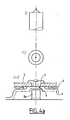
- FIGS. 4a, 4b and 4c illustrate various shapes that can be envisaged for the punch 8.
- it may be of the tip type (FIG. 4a), the flat type (FIG. 4b) or the pyramid type (FIG. 4c). according to the shape which is to be given to the pin head 4.
- FIG. 4a, iii) an anvil 8a is also shown, on which the sole 1 is placed and which serves to prevent deformation. of said sole 1 when the punch 8 crushes the pin 4.
- the pins or pins that has a range 3 provide three functions: crimping, mass recovery, centering, the same pawn or pin can perform many of these functions.
- the printed circuit board 2 and the layer 6 may be pre-assembled, before the equipment of said card 2 components.
- the layer 6 can be pe-assembled on the sole 1.
- the crimping orifices 5 may be reinforced by a layer 10 extending in said orifices and on the edges thereof.
- This reinforcement 10 may be insulating or conductive. In the case where it is conductive, it can be used to ensure a resumption of mass between the metal plate 1 and the face of the printed circuit board 2 which is opposite said sole 1. It is then for example constituted by a metallization in copper.
- the printed circuit board 2 may receive other components than surface-mount components and in particular through-going components 11.
- the printed circuit board 2 is a double-sided card receiving one or more CMS 13 components brazed on its face directly opposite the soleplate 1.
- the sole 1 then advantageously has a counter form 12 to the right of said component 13.
- the sole 1 may have cooling fins 16 extending to the bearing surfaces 3, projecting from the face of the sole 1 which is opposite the card 2 printed circuit board.
- FIGS. 10 and 11 illustrate an assembly of the type of those described with reference to FIGS. 1 to 7, supplemented by shielding elements.
- shielding elements comprise in particular a shielding cap 14 which is attached to the sole 1 and which covers the printed circuit board (2) and the layer 6 of thermally conductive and electrically insulating material.
- They further comprise a partition metal partition 15 on the map 2 to isolate two areas thereof.
- This partition metal partition 15 extends over substantially the entire width of said card 2.
- the printed circuit board 2 may be a multi-layer board, having a ground plane which is connected to the metal partition wall 15 or to a ground track that the board has.
- the two parts 17a, 17b delimited by the metal separation partition 15 on the card 2 carry one of the power components of the control module, the other of the control components and in particular a management microprocessor.
- the part carrying the power components is connected, by means of a shielded cable 18 articulated on the shielding cap 14, to the discharge lamp or to other power means which supply it.
- the metal separation partition 15 extends through the printed circuit board 2 to the metal base 1 to define therewith and the shielding cap 14 two boxes isolated from each other electromagnetic disturbances that they breed. Thus, there are two separate shield boxes 17a, 17b.
- the signals passing from one of these bays 17a, 17b to the other may be filtered at the metal partition wall 15 by filtering means provided for this purpose (capacity, filter Rc ).
- a ground resumption is provided between the shielding cap 14 and said shielded cable 18, for example by a resilient metal part interposed between the two or by a resilient tab that has the shielding cap 14. This shielding recovery ensures continuity between the control module and the discharge lamp.
- the shielding cap 14 is fixed on the sole 1 by crimping.
- This feature makes the assembly particularly suitable for use with a motor vehicle headlight discharge lamp control module.
- the sole 1 may comprise for this purpose on its edges a plurality of holes, referenced 19 in Figures 11 and 12, for fixing in a projector assembly.
- FIG 12 there is illustrated an assembly comprising an assembly according to those just described fixed by screws 21 on a housing 20 projector.
- a seal 22 carried by the sole 1 and surrounding the shielding cap 14 is interposed between said housing 20 and the assembly.
- the zone of the assembly which is sealed is that which is illustrated by a double arrow in FIG.
Landscapes
- Engineering & Computer Science (AREA)
- Microelectronics & Electronic Packaging (AREA)
- Physics & Mathematics (AREA)
- Thermal Sciences (AREA)
- Manufacturing & Machinery (AREA)
- Cooling Or The Like Of Electrical Apparatus (AREA)
- Non-Portable Lighting Devices Or Systems Thereof (AREA)
Claims (10)
- Baugruppe mit einer eine Wärmesenke bildenden Metallplatte (1) sowie einer von der Metallplatte (1) getragenen Leiterplatte (2),
dadurch gekennzeichnet, dass die Metallplatte (1) wenigstens zwei Auflageflächen (3) aufweist, die bezüglich der restlichen Metallplatte (1) geringfügig vorstehen und auf denen die Leiterplatte (2) aufliegt, wobei die Auflageflächen (3) wenigstens einen Crimpstift (4) aufweisen, der mit einer komplementären Öffnung (5) zusammenwirkt, die die Leiterplatte (2) aufweist, um die Leiterplatte (2) auf der Metallplatte (1) zu befestigen, und dass eine Schicht (6) eines thermisch leitenden und elektrisch isolierenden Materials in den Bereichen zwischen den Auflageflächen (3) durch eingefügt sein zwischen der Leiterplatte (2) und der Metallplatte (1) angeordnet ist, wobei die Leiterplatte (2) und die Metallplatte (1) auf die Schicht (6) aus thermisch leitendem und elektrisch isolierendem Material eine Druckbeanspruchung ausüben. - Baugruppe nach Anspruch 1,
dadurch gekennzeichnet, dass die Leiterplatte (2) wenigstens einen thermischen Pfad (9) aufweist, in dem das thermisch leitende und elektrisch isolierende Material der Schicht (6) aufgenommen ist. - Baugruppe nach Anspruch 2,
dadurch gekennzeichnet, dass wenigstens eine Crimpöffnung (5) der Leiterplatte (2) durch eine Schicht (10) verstärkt ist, die in dieser Öffnung und auf deren Rändern verläuft. - Baugruppe nach Anspruch 3,
dadurch gekennzeichnet, dass die Schicht (10) eine Kontaktierungsschicht ist, die durch Kontakt mit dem Crimpstift (4) eine Masseverbindung zwischen der Metallplatte (1) und der Leiterplatte (2) gewährleistet. - Baugruppe nach einem der vorhergehenden Ansprüche,
dadurch gekennzeichnet, dass die Metallplatte (1) wenigstens eine Gegenform (12) aufweist, um wenigstens ein Teil eines Bauteils (13) aufzunehmen, das von der Leiterplatte (2) zur Metallplatte (1) vorstehend verläuft. - Baugruppe nach einem der vorhergehenden Ansprüche,
dadurch gekennzeichnet, dass die Metallplatte (1) rechtwinklig zu einer Auflagefläche (3) Kühlflügel (16) umfasst, die bezüglich der Seite der Metallplatte (1), die der Leiterplatte (2) gegenüberliegt, vorstehend verlaufen. - Baugruppe nach einem der vorhergehenden Ansprüche,
dadurch gekennzeichnet, dass sie eine Abschirmkappe (14) umfasst, die auf der Metallplatte (1) aufgesetzt ist, um die Leiterplatte (2) und die Schicht (6) aus thermisch leitendem und elektrisch isolierendem Material zu bedecken. - Baugruppe nach einem der vorhergehenden Ansprüche,
dadurch gekennzeichnet, dass sie eine Metalltrennwand (15) aufweist und die Leiterplatte (2) auf einer Seite der Metalltrennwand (15) eine Steuerelektronik mit insbesondere einem Mikroprozessor und auf der anderen Seite der Metalltrennwand (15) eine Leistungselektronik trägt. - Baugruppe nach Anspruch 8,
dadurch gekennzeichnet, dass sich die Metalltrennwand (15) durch die Leiterkarte hindurch bis zur Metallplatte (1) ausdehnt, um mit dieser und der Abschirmkappe (14) zwei Kammern zu bilden, die insbesondere vor elektromagnetischen Störungen voneinander isoliert sind. - Steuermodul für Kraftfahrzeug-Entladungslampe,
dadurch gekennzeichnet, dass es eine Baugruppe nach einem der vorhergehenden Ansprüche umfasst.
Applications Claiming Priority (2)
| Application Number | Priority Date | Filing Date | Title |
|---|---|---|---|
| FR9911828A FR2798814B1 (fr) | 1999-09-22 | 1999-09-22 | Perfectionnements aux assemblages electroniques a drain thermique, notamment pour module de commande de lampe a decharge de projecteur de vehicule automobile |
| FR9911828 | 1999-09-22 |
Publications (2)
| Publication Number | Publication Date |
|---|---|
| EP1087652A1 EP1087652A1 (de) | 2001-03-28 |
| EP1087652B1 true EP1087652B1 (de) | 2006-07-26 |
Family
ID=9550111
Family Applications (1)
| Application Number | Title | Priority Date | Filing Date |
|---|---|---|---|
| EP00402504A Expired - Lifetime EP1087652B1 (de) | 1999-09-22 | 2000-09-12 | Verbesserungen für gekühlte elektronische Baugruppen, insbesondere für Steuerungsmodul eines Kraftfahrzeugscheinwerfers |
Country Status (6)
| Country | Link |
|---|---|
| US (1) | US6347038B1 (de) |
| EP (1) | EP1087652B1 (de) |
| JP (1) | JP4511705B2 (de) |
| DE (1) | DE60029527T2 (de) |
| ES (1) | ES2269083T3 (de) |
| FR (1) | FR2798814B1 (de) |
Families Citing this family (22)
| Publication number | Priority date | Publication date | Assignee | Title |
|---|---|---|---|---|
| DE10214311A1 (de) * | 2002-03-28 | 2003-10-09 | Marconi Comm Gmbh | Kühlanordnung für ein elektronisches Bauelement |
| DE10300175B4 (de) * | 2003-01-08 | 2016-12-29 | Hella Kgaa Hueck & Co. | Elektronische Baugruppe mit Wärme ableitendem Gehäuseteil |
| US6999318B2 (en) * | 2003-07-28 | 2006-02-14 | Honeywell International Inc. | Heatsinking electronic devices |
| FR2872992B1 (fr) * | 2004-07-09 | 2006-09-29 | Valeo Vision Sa | Assemblage electronique a drain thermique notamment pour module de commande de lampe a decharge de projecteurs de vehicule automobile |
| FR2922078B1 (fr) * | 2007-10-08 | 2011-04-15 | Valeo Vision | Module electronique comportant un connecteur blinde fixe sur une carte a circuit integre par l'intermediaire d'une patte de fixation du blindage |
| DE102008029410A1 (de) * | 2008-06-23 | 2009-12-24 | Brose Fahrzeugteile GmbH & Co. Kommanditgesellschaft, Würzburg | Vorrichtung, insbesondere zur Stromleitung, und ein Verfahren zur Herstellung einer Vorrichtung, insbesondere zur Stromleitung |
| FR2933567B1 (fr) * | 2008-07-04 | 2010-09-10 | Valeo Vision Sas | Dispositif d'assemblage par sertissage d'un module electronique de commande pour projecteur de vehicule automobile |
| FR2936646B1 (fr) * | 2008-10-01 | 2011-07-22 | Jean Jacques Carrillo | Disjoncteur electronique en tranche et installation le comportant. |
| CN102362561B (zh) * | 2009-03-30 | 2015-08-19 | 赤多尼科两合股份有限公司 | 具有集成散热板的驱动装置 |
| FR2951048A1 (fr) * | 2009-10-07 | 2011-04-08 | Valeo Vision | Module de commande electronique pour un dispositif d'eclairage et/ou signalisation de vehicule |
| US8581454B2 (en) * | 2010-01-11 | 2013-11-12 | Pro-Dex, Inc. | Handheld device with thermal padding |
| FR2971113B1 (fr) * | 2010-11-25 | 2013-11-22 | Valeo Vision | Procede d'assemblage, par soudage laser, d'une carte electronique a une partie d'un boitier d'un module de commande d'un dispositif d'eclairage et/ou de signalisation d'un vehicule automobile. |
| WO2014001957A1 (en) * | 2012-06-28 | 2014-01-03 | Koninklijke Philips N.V. | Assembly for transferring and dissipating heat |
| US8995933B2 (en) | 2013-06-21 | 2015-03-31 | Motorola Solutions, Inc. | Radio frequency transistor and matching circuit grounding and thermal management apparatus |
| FR3045829B1 (fr) * | 2015-12-18 | 2017-12-29 | Continental Automotive France | Procede de controle de l'assemblage par rivetage d'un circuit imprime |
| EP3565395B1 (de) * | 2016-12-28 | 2022-03-16 | Mitsubishi Electric Corporation | Stromversorgungsvorrichtung |
| EP3817529B1 (de) | 2018-06-27 | 2023-10-04 | Mitsubishi Electric Corporation | Stromversorgungsvorrichtung |
| EP3629687A1 (de) * | 2018-09-26 | 2020-04-01 | Siemens Aktiengesellschaft | Verfahren für eine montage eines elektrischen geräts |
| EP3629686A1 (de) * | 2018-09-26 | 2020-04-01 | Siemens Aktiengesellschaft | Vorrichtung zum anpressen von bauelementen |
| FR3115718A1 (fr) * | 2020-11-03 | 2022-05-06 | Vitesco Technologies | Procédé de positionnement d’un élément par rapport à une tôle et dispositif correspondant |
| CN118959786A (zh) * | 2023-05-15 | 2024-11-15 | 富联精密电子(天津)有限公司 | 支撑螺栓、悬臂支撑结构及传导装置 |
| DE102023204543A1 (de) * | 2023-05-15 | 2024-11-21 | Volkswagen Aktiengesellschaft | Bauteilanordnung sowie Werkzeug und Verfahren zur Herstellung einer solchen Bauteilanordnung |
Family Cites Families (17)
| Publication number | Priority date | Publication date | Assignee | Title |
|---|---|---|---|---|
| FR2615347B1 (fr) * | 1987-05-15 | 1993-07-23 | Neiman Sa | Module de puissance pour equipements automobiles |
| US4974119A (en) * | 1988-09-14 | 1990-11-27 | The Charles Stark Draper Laboratories, Inc. | Conforming heat sink assembly |
| JPH0317024U (de) * | 1989-07-03 | 1991-02-20 | ||
| JPH03175698A (ja) * | 1989-12-04 | 1991-07-30 | Mitsubishi Electric Corp | プリント配線板 |
| DE59005035D1 (de) * | 1990-12-12 | 1994-04-21 | Siemens Ag | Leiterplatte für elektronische Steuergeräte und Verfahren zum Herstellen einer solchen Leiterplatte. |
| US5367434A (en) * | 1993-05-06 | 1994-11-22 | Motorola, Inc. | Electrical module assembly |
| JPH0856086A (ja) * | 1994-08-12 | 1996-02-27 | Fujitsu Ten Ltd | 配線基板の部材への取付構造 |
| EP0735551B1 (de) * | 1995-03-29 | 2002-02-27 | Valeo Electronique | Transformatoreinrichtung, insbesondere für eine Versorgungseinrichtung von Entladungslampen in Kraftfahrzeugen |
| DE19528632A1 (de) * | 1995-08-04 | 1997-02-06 | Bosch Gmbh Robert | Steuergerät bestehend aus mindestens zwei Gehäuseteilen |
| DE19532992A1 (de) * | 1995-09-07 | 1997-03-13 | Telefunken Microelectron | Leiterplatte |
| FR2742294B1 (fr) * | 1995-12-11 | 1998-02-27 | Valeo Electronique | Assemblage electronique a drain thermique, notamment pour transformateur haute tension de lampe a decharge de projecteur de vehicule automobile |
| WO1998054735A1 (de) * | 1997-05-27 | 1998-12-03 | Melcher Ag | Vorrichtung und verfahren zum kühlen einer planarinduktivität |
| JPH1140901A (ja) * | 1997-07-23 | 1999-02-12 | Sharp Corp | 回路基板 |
| DE19750433A1 (de) * | 1997-11-14 | 1999-06-02 | Telefunken Microelectron | Verfahren zur Erzeugung einer Montageplatte |
| JPH11163564A (ja) * | 1997-11-25 | 1999-06-18 | Canon Inc | 電子機器及び電子機器の製造方法 |
| FR2784001B1 (fr) | 1998-09-30 | 2001-05-04 | Valeo Electronique | Cloison de blindage pour dispositif a carte a circuit imprime et capot de blindage |
| TW399309B (en) * | 1998-09-30 | 2000-07-21 | World Wiser Electronics Inc | Cavity-down package structure with thermal via |
-
1999
- 1999-09-22 FR FR9911828A patent/FR2798814B1/fr not_active Expired - Lifetime
-
2000
- 2000-09-12 DE DE60029527T patent/DE60029527T2/de not_active Expired - Lifetime
- 2000-09-12 EP EP00402504A patent/EP1087652B1/de not_active Expired - Lifetime
- 2000-09-12 ES ES00402504T patent/ES2269083T3/es not_active Expired - Lifetime
- 2000-09-22 US US09/667,886 patent/US6347038B1/en not_active Expired - Lifetime
- 2000-09-22 JP JP2000288269A patent/JP4511705B2/ja not_active Expired - Lifetime
Also Published As
| Publication number | Publication date |
|---|---|
| FR2798814A1 (fr) | 2001-03-23 |
| EP1087652A1 (de) | 2001-03-28 |
| JP4511705B2 (ja) | 2010-07-28 |
| DE60029527D1 (de) | 2006-09-07 |
| DE60029527T2 (de) | 2007-03-08 |
| ES2269083T3 (es) | 2007-04-01 |
| JP2001135963A (ja) | 2001-05-18 |
| US6347038B1 (en) | 2002-02-12 |
| FR2798814B1 (fr) | 2001-11-16 |
Similar Documents
| Publication | Publication Date | Title |
|---|---|---|
| EP1087652B1 (de) | Verbesserungen für gekühlte elektronische Baugruppen, insbesondere für Steuerungsmodul eines Kraftfahrzeugscheinwerfers | |
| EP0578520B1 (de) | Modularer Einschub-Leiterplattenträger für Baugruppenträger | |
| EP3551501B1 (de) | Wärmeableitungsvorrichtung für eine multimedia-steuereinheit | |
| EP1504636B1 (de) | Gekühlter leistungsschalter | |
| FR3018989A1 (fr) | Module electronique, notamment pour un appareil de commande de boite de vitesses | |
| FR2667452A1 (fr) | Connecteur de circuit imprime. | |
| FR2589031A1 (fr) | Agencement de groupes d'elements de circuits supportant des composants electriques et de refroidissement | |
| FR2560731A1 (fr) | Carte imprimee multicouche thermoconductrice | |
| FR2675632A1 (fr) | Dispositif de conditionnement de circuits integres. | |
| EP0233674A1 (de) | Informationsbus-Verbinder | |
| EP2891178B1 (de) | Körper zum pressen eines teils auf eine oberfläche | |
| EP0291400B1 (de) | Leistungsmodul für Fahrzeuganlagen | |
| EP2536261B1 (de) | Elektronisches Leistungsmodul mit integrierter Kapazität | |
| EP4345577A1 (de) | Kühlkörper für eine berechnungsblatt-array-karte | |
| EP0575606B1 (de) | Gehäuse für wärmeerzeugende elektronische bauteile. | |
| EP1116424B1 (de) | Elektronische baugruppe mit einer wärmeplatte | |
| FR2518813A1 (fr) | Support d'interconnexion d'un boitier de circuit integre sur un circuit imprime et systeme d'interconnexion utilisant un tel support | |
| EP1054445A1 (de) | Elektronisches Gehäuse auf einer Leiterplatte sowie Verfahren zu seiner Herstellung | |
| FR2794299A1 (fr) | Porte-balais a composant de commande pour alternateur de vehicule automobile | |
| EP2362720A1 (de) | Elektronisches module und elektronische Anordnung umfassend dieses Modul | |
| EP0734066B1 (de) | Elektronischer Leistungsmodul | |
| FR2839607A1 (fr) | Assemblage de composants de puissance sur un circuit imprime ainsi qu'un procede d'obtention d'un tel assemblage | |
| FR2861949A1 (fr) | Dispositif de commutation de puissance refroidi a entretoise de resine et son procede de fabrication | |
| FR2907266A1 (fr) | Dispositif de raccordement electrique notamment pour panneau solaire electrique | |
| FR2764473A1 (fr) | Tiroir electronique comportant un dispositif ameliore d'evacuation de chaleur |
Legal Events
| Date | Code | Title | Description |
|---|---|---|---|
| PUAI | Public reference made under article 153(3) epc to a published international application that has entered the european phase |
Free format text: ORIGINAL CODE: 0009012 |
|
| AK | Designated contracting states |
Kind code of ref document: A1 Designated state(s): AT BE CH CY DE DK ES FI FR GB GR IE IT LI LU MC NL PT SE |
|
| AX | Request for extension of the european patent |
Free format text: AL;LT;LV;MK;RO;SI |
|
| 17P | Request for examination filed |
Effective date: 20010926 |
|
| AKX | Designation fees paid |
Free format text: DE ES GB IT |
|
| GRAP | Despatch of communication of intention to grant a patent |
Free format text: ORIGINAL CODE: EPIDOSNIGR1 |
|
| GRAS | Grant fee paid |
Free format text: ORIGINAL CODE: EPIDOSNIGR3 |
|
| GRAA | (expected) grant |
Free format text: ORIGINAL CODE: 0009210 |
|
| AK | Designated contracting states |
Kind code of ref document: B1 Designated state(s): DE ES GB IT |
|
| REG | Reference to a national code |
Ref country code: GB Ref legal event code: FG4D Free format text: NOT ENGLISH |
|
| REF | Corresponds to: |
Ref document number: 60029527 Country of ref document: DE Date of ref document: 20060907 Kind code of ref document: P |
|
| GBT | Gb: translation of ep patent filed (gb section 77(6)(a)/1977) |
Effective date: 20060923 |
|
| REG | Reference to a national code |
Ref country code: ES Ref legal event code: FG2A Ref document number: 2269083 Country of ref document: ES Kind code of ref document: T3 |
|
| PLBE | No opposition filed within time limit |
Free format text: ORIGINAL CODE: 0009261 |
|
| STAA | Information on the status of an ep patent application or granted ep patent |
Free format text: STATUS: NO OPPOSITION FILED WITHIN TIME LIMIT |
|
| 26N | No opposition filed |
Effective date: 20070427 |
|
| PGFP | Annual fee paid to national office [announced via postgrant information from national office to epo] |
Ref country code: DE Payment date: 20170911 Year of fee payment: 18 Ref country code: IT Payment date: 20170918 Year of fee payment: 18 Ref country code: GB Payment date: 20170914 Year of fee payment: 18 |
|
| PGFP | Annual fee paid to national office [announced via postgrant information from national office to epo] |
Ref country code: ES Payment date: 20171016 Year of fee payment: 18 |
|
| REG | Reference to a national code |
Ref country code: DE Ref legal event code: R119 Ref document number: 60029527 Country of ref document: DE |
|
| GBPC | Gb: european patent ceased through non-payment of renewal fee |
Effective date: 20180912 |
|
| PG25 | Lapsed in a contracting state [announced via postgrant information from national office to epo] |
Ref country code: IT Free format text: LAPSE BECAUSE OF NON-PAYMENT OF DUE FEES Effective date: 20180912 Ref country code: DE Free format text: LAPSE BECAUSE OF NON-PAYMENT OF DUE FEES Effective date: 20190402 |
|
| REG | Reference to a national code |
Ref country code: ES Ref legal event code: FD2A Effective date: 20191030 |
|
| PG25 | Lapsed in a contracting state [announced via postgrant information from national office to epo] |
Ref country code: GB Free format text: LAPSE BECAUSE OF NON-PAYMENT OF DUE FEES Effective date: 20180912 |
|
| PG25 | Lapsed in a contracting state [announced via postgrant information from national office to epo] |
Ref country code: ES Free format text: LAPSE BECAUSE OF NON-PAYMENT OF DUE FEES Effective date: 20180913 |