EP1085315A1 - Integrierter optischer Sensor - Google Patents
Integrierter optischer Sensor Download PDFInfo
- Publication number
- EP1085315A1 EP1085315A1 EP99118309A EP99118309A EP1085315A1 EP 1085315 A1 EP1085315 A1 EP 1085315A1 EP 99118309 A EP99118309 A EP 99118309A EP 99118309 A EP99118309 A EP 99118309A EP 1085315 A1 EP1085315 A1 EP 1085315A1
- Authority
- EP
- European Patent Office
- Prior art keywords
- electromagnetic radiation
- grating
- waveguide structure
- freedom
- resonant waveguide
- Prior art date
- Legal status (The legal status is an assumption and is not a legal conclusion. Google has not performed a legal analysis and makes no representation as to the accuracy of the status listed.)
- Granted
Links
- 239000000126 substance Substances 0.000 claims abstract description 31
- 230000005670 electromagnetic radiation Effects 0.000 claims description 34
- 230000010287 polarization Effects 0.000 claims description 26
- 230000001678 irradiating effect Effects 0.000 claims description 14
- 230000008878 coupling Effects 0.000 claims description 13
- 238000010168 coupling process Methods 0.000 claims description 13
- 238000005859 coupling reaction Methods 0.000 claims description 13
- 238000000034 method Methods 0.000 claims description 12
- 238000004020 luminiscence type Methods 0.000 claims description 8
- 238000010521 absorption reaction Methods 0.000 claims description 5
- 238000000151 deposition Methods 0.000 claims description 3
- 230000005672 electromagnetic field Effects 0.000 claims description 3
- 230000003993 interaction Effects 0.000 claims description 2
- 238000000926 separation method Methods 0.000 abstract description 15
- 230000005284 excitation Effects 0.000 description 18
- 230000003287 optical effect Effects 0.000 description 11
- 230000001965 increasing effect Effects 0.000 description 8
- 238000001514 detection method Methods 0.000 description 7
- 239000000758 substrate Substances 0.000 description 7
- GWEVSGVZZGPLCZ-UHFFFAOYSA-N Titan oxide Chemical compound O=[Ti]=O GWEVSGVZZGPLCZ-UHFFFAOYSA-N 0.000 description 6
- 230000008901 benefit Effects 0.000 description 6
- 239000000872 buffer Substances 0.000 description 5
- 238000009826 distribution Methods 0.000 description 5
- 238000002474 experimental method Methods 0.000 description 5
- 230000000694 effects Effects 0.000 description 4
- 239000000243 solution Substances 0.000 description 4
- 239000012491 analyte Substances 0.000 description 3
- 239000003153 chemical reaction reagent Substances 0.000 description 3
- 238000005286 illumination Methods 0.000 description 3
- 238000005259 measurement Methods 0.000 description 3
- 238000003556 assay Methods 0.000 description 2
- 230000006872 improvement Effects 0.000 description 2
- 239000000463 material Substances 0.000 description 2
- 239000004033 plastic Substances 0.000 description 2
- 239000004417 polycarbonate Substances 0.000 description 2
- 229920000515 polycarbonate Polymers 0.000 description 2
- 230000008569 process Effects 0.000 description 2
- 230000005855 radiation Effects 0.000 description 2
- 230000035945 sensitivity Effects 0.000 description 2
- 238000001069 Raman spectroscopy Methods 0.000 description 1
- 230000003321 amplification Effects 0.000 description 1
- 238000013459 approach Methods 0.000 description 1
- 230000000903 blocking effect Effects 0.000 description 1
- 239000007853 buffer solution Substances 0.000 description 1
- 230000008021 deposition Effects 0.000 description 1
- 230000003292 diminished effect Effects 0.000 description 1
- 238000005516 engineering process Methods 0.000 description 1
- 230000002708 enhancing effect Effects 0.000 description 1
- 230000007613 environmental effect Effects 0.000 description 1
- 238000000605 extraction Methods 0.000 description 1
- 239000011521 glass Substances 0.000 description 1
- 238000003384 imaging method Methods 0.000 description 1
- 239000007788 liquid Substances 0.000 description 1
- 238000003199 nucleic acid amplification method Methods 0.000 description 1
- 230000001902 propagating effect Effects 0.000 description 1
- 230000009467 reduction Effects 0.000 description 1
- 229920006395 saturated elastomer Polymers 0.000 description 1
- 230000007480 spreading Effects 0.000 description 1
- 230000001629 suppression Effects 0.000 description 1
- 238000012546 transfer Methods 0.000 description 1
Images


Classifications
-
- G—PHYSICS
- G01—MEASURING; TESTING
- G01N—INVESTIGATING OR ANALYSING MATERIALS BY DETERMINING THEIR CHEMICAL OR PHYSICAL PROPERTIES
- G01N21/00—Investigating or analysing materials by the use of optical means, i.e. using sub-millimetre waves, infrared, visible or ultraviolet light
- G01N21/62—Systems in which the material investigated is excited whereby it emits light or causes a change in wavelength of the incident light
- G01N21/63—Systems in which the material investigated is excited whereby it emits light or causes a change in wavelength of the incident light optically excited
- G01N21/64—Fluorescence; Phosphorescence
- G01N21/645—Specially adapted constructive features of fluorimeters
- G01N21/648—Specially adapted constructive features of fluorimeters using evanescent coupling or surface plasmon coupling for the excitation of fluorescence
-
- G—PHYSICS
- G01—MEASURING; TESTING
- G01N—INVESTIGATING OR ANALYSING MATERIALS BY DETERMINING THEIR CHEMICAL OR PHYSICAL PROPERTIES
- G01N21/00—Investigating or analysing materials by the use of optical means, i.e. using sub-millimetre waves, infrared, visible or ultraviolet light
- G01N21/62—Systems in which the material investigated is excited whereby it emits light or causes a change in wavelength of the incident light
- G01N21/63—Systems in which the material investigated is excited whereby it emits light or causes a change in wavelength of the incident light optically excited
- G01N21/64—Fluorescence; Phosphorescence
- G01N21/6428—Measuring fluorescence of fluorescent products of reactions or of fluorochrome labelled reactive substances, e.g. measuring quenching effects, using measuring "optrodes"
-
- G—PHYSICS
- G01—MEASURING; TESTING
- G01N—INVESTIGATING OR ANALYSING MATERIALS BY DETERMINING THEIR CHEMICAL OR PHYSICAL PROPERTIES
- G01N21/00—Investigating or analysing materials by the use of optical means, i.e. using sub-millimetre waves, infrared, visible or ultraviolet light
- G01N21/75—Systems in which material is subjected to a chemical reaction, the progress or the result of the reaction being investigated
- G01N21/77—Systems in which material is subjected to a chemical reaction, the progress or the result of the reaction being investigated by observing the effect on a chemical indicator
- G01N21/7703—Systems in which material is subjected to a chemical reaction, the progress or the result of the reaction being investigated by observing the effect on a chemical indicator using reagent-clad optical fibres or optical waveguides
- G01N21/774—Systems in which material is subjected to a chemical reaction, the progress or the result of the reaction being investigated by observing the effect on a chemical indicator using reagent-clad optical fibres or optical waveguides the reagent being on a grating or periodic structure
- G01N21/7743—Systems in which material is subjected to a chemical reaction, the progress or the result of the reaction being investigated by observing the effect on a chemical indicator using reagent-clad optical fibres or optical waveguides the reagent being on a grating or periodic structure the reagent-coated grating coupling light in or out of the waveguide
Definitions
- This invention relates to an integrated-optical chemical and/or biochemical sensor and to a method for integrated-optically sensing a chemical and/or biochemical substance.
- biochemical microsystems especially for application areas such as medical, food and environmental, require the detection of several analytes being simultaneously present in a liquid.
- IO integrated optical
- CSEM WO 92/19976
- R.E. Kunz "Totally Integrated Optical Measuring Sensors," Proc. SPIE, Vol. 1587, 98-113 (1992); WO 96/35940 (Ciba-Geigy).
- This invention deals with a subclass of sensors based on amplitude effects, i.e. those where the amplitudes of light waves (guided or/and freely propagating) are changed by the effect to be measured. Examples are luminescence (e.g. fluorescence, (electro-)chemo-luminescence), absorption or scattering (e.g. elastic and Raman).
- luminescence e.g. fluorescence, (electro-)chemo-luminescence
- absorption or scattering e.g. elastic and Raman
- Sensing signal and referencing pads are both denoted by the term "measuring pad” in this document.
- This invention aims at removing the drawbacks of the state-of-the art solutions for achieving amplitude-based high-density array sensors by reducing the area required for performing the sensing task, especially by reducing the area required by a single measuring pad in an array, and by increasing the ratio between active and passive chip area.
- the integrated-optical chemical and/or biochemical sensor according to the invention comprises
- Said irradiating means and/or said outcoupling means preferably comprise grating structures.
- Said first and second set of degrees of freedom preferably comprises the diffraction order, the polarization, the guided-mode order, the grating vector and/or the planes of incidence and excidence.
- the method according to the invention for integrated-optically sensing a chemical and/or biochemical substance using a resonant waveguide structure comprises the steps of
- the interaction of said substance with said first electromagnetic radiation preferably comprises luminescence, scattering, absorption, chemiluminescence and/or electrochemi-luminescence.
- Said first and second set of degrees of freedom preferably comprises the diffraction order, the polarization, the guided-mode order, the grating vector and/or the planes of incidence and excidence.
- sensing pads results for single-chip sensors, leading to several advantages as is described below.
- An important improvement is achieved for on-chip referencing, which is eased due to the smaller distance between measuring pads, and because multiple referencing pads can be used per sensing pad, e.g. one on top and one below or left and right or distributed around etc. This is especially important for sensors with very high sensitivities, since they are more affected by unspecific effects such as temperature and signal drift due to chemical and physical fluctuations.
- the sensor according to the invention can be combined with known integrated-optical sensors based on other principles such as refractometry, for example using an integrated-optical light pointer (see, e.g., R.E. Kunz, "Miniature integrated optical modules for chemical and biochemical sensing", Sensors and Actuators B 38-39 (1997) 13-28, which is incorporated herein by reference).
- integrated-optical light pointer see, e.g., R.E. Kunz, "Miniature integrated optical modules for chemical and biochemical sensing", Sensors and Actuators B 38-39 (1997) 13-28, which is incorporated herein by reference).
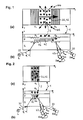
- a fluorescence-based sensor is depicted in Figure 1 , where (a) is a top view and (b) is a side view or a cross-section.
- the sensor comprises a waveguide 1 with a substrate S, e.g., made of plastic or glass material, and a waveguiding film F, e.g., made of TiO 2 .
- the waveguide 1 is at least partially covered by a cover medium (or a sensing medium) C.
- a light source L e.g., a laser, emits light 31 which is directed towards the sensor.
- a first grating coupler G 1 on or in the waveguide 1 is used to couple the incident light wave u i , 31, into the waveguide 1 under an incoupling angle ⁇ i .
- Fluorescent (emitted) light 42 is, at least partially, also guided in the waveguide 1 and then coupled out by means of a second grating coupler G 2 as a light wave u em , 43, under an outcoupling angle ⁇ em , whereas the exciting light is coupled out as a light wave u ex , 33, under a different outcoupling angle ⁇ ex ; in the example of Fig. 1, ⁇ em ⁇ ⁇ ex .
- the light waves u em , u ex i.e., their intensities and/or their local intensity distributions, are detected by means of detectors Det em , Det ex , respectively.
- the sensor according to Fig. 1 does not show the features defined in the claims and has the following drawbacks:
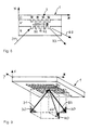
- Figure 2 shows an improved sensor where the molecules 2 to be measured are placed directly on the grating coupler G, and the readout is also performed by the same grating G.
- This sensor requires a smaller area than the arrangement of Fig. 1.
- the efficiency is higher than with the arrangement of Fig. 1.
- the crosstalk problem remains the same if the measures according to the invention are not applied.
- the arrangement of Figure 3 is similar to that of Fig. 2, but the fluorescent light is coupled out in two symmetric output diffraction orders 43.1 and 43.2, e.g., in the +1 st and in the -1 st order, respectively.
- the fluorescent light 43.1, 43.2 typically does not show one single well-defined wavelength, but rather a certain wavelength distribution depending on the characteristics of the fluorescent molecules. Therefore, the fluorescent light 43.1, 43.2 is coupled out under a certain distribution of angles of excidence, which is sketched by dashed lines. Another reason for the spreading of the outcoupled light 43.1, 43.2 is scattering, mainly in the region of the molecules 2.
- the light path is on the side of the molecules 2, whereas in the arrangement of Figure 3, it is on the side of the substrate S. Therefore, the substrate S may be opaque in the case of Fig. 4.
- the sensing region G is preferably covered by cover means 5, e.g., made of plastic material, in which a recess or a channel 51 for the sensing region G is formed.
- FIG. 5 shows an arrangement of a multisensor.
- Each grating pad G 11 , G 12 , ..., G 21 , G 22 , ... corresponds to a measurement zone.
- the reading of a multisensor of this type can be made in parallel (one collimated beam, one wavelength imaging of the surface on a camera) or sequentially. In the latter case there are at least two possibilities: i) a small collimated (or slightly focused) beam moved from one grating pad to the other, or ii) a large collimated beam and different grating period for each pad; the sequential reading can be made either by changing the coupling angle or by changing the wavelength of the incident light.
- the sensors shown in Figures 1-5 may be conventional fluorescence sensors, or they may show the features according to the invention. These features are explained in detail in the following figures. For reasons of clarity, some features already introduced in Figures 1-5, such as the light source L, are not shown in the following figures.
- One measuring pad of the sensor according to the invention preferably comprises one single grating G on or in a waveguide structure 1, as shown in Figure 6 .
- Molecules 2 to be sensed are deposited on the grating G.
- the incident guided light 32 interacts with the fluorescent molecules 2, which emit light 42 of a longer wavelength.
- a part of the emitted light 42 excites a resonant electromagnetic field in the waveguide structure 1 and is coupled out from the waveguide structure 1 by the grating G.
- "Clearly separated” means in this document separated in such a way that it can be detected without any special measures; for practical purposes, a "clear separation" is achieved if the angles of excidence differ by at least about 5°.
- the dashed lines indicate that fluorescent light 43 is coupled out under a certain distribution of angles of excidence.
- m g,em ⁇ 1.
- emitted light 43.2 having a polarization which differs from the polarization of the exciting light 33 is coupled out of the waveguide structure 1, as shown in Figure 7 .
- the diffraction order may be the same as or other than that of the incident light 31.
- the emitted light 43.2 can clearly be separated from other light 33.
- the diffraction order and the polarization may be the same as or other than that of the outcoupled exciting light 33; in any case, the two outcoupled light components 43, 33 will be clearly separated.
- Figures 9 and 10 show a fourth embodiment of a sensor according to the invention. It comprises a grating coupler composed of two superposed subgratings G 1 , G 2 .
- the first subgrating G 1 has a grating vector in z direction, i.e., lines parallel to the y direction, and is used for incoupling the exciting light 31.
- the second subgrating G 2 is perpendicular to the first subgrating and is used for outcoupling emitted light 44. This is possible because there is emitted light 44 with components in y (or -y) direction (cf. Fig. 1).
- the outcoupled emitted light 43 does not propagate in the same first plane 30 as the incident light 31 and the outcoupled exciting light 33, but in a second plane 40 which is perpendicular to the first plane 30. With this arrangement, it is possible to very efficiently separate outcoupled emitted light 43 from outcoupled exciting light 33, thus increasing the signal-to-noise ratio.
- the sensor of Figure 11 uses a circular (and possibly focusing) grating G to collect the fluorescent light 44 more efficiently, thus reducing the area of biocoated surface and crosstalk between different measuring pads G 11 , G 12 , ..., G 21 , G 22 , ... of a multisensor (cf. Fig. 5).
- the molecules 2 are directly placed on a circular grating coupler pad G.
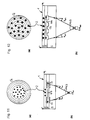
- Figure 13 shows (non-resonant or partially resonant) excitation with a broadband light source L, e.g., a light-emitting diode (LED).
- a broadband light source L e.g., a light-emitting diode (LED).
- Figures 14 and 15 show embodiments of the optical arrangement with further possibilities of non-resonantly or partially resonantly exciting fluorescence.
- the exciting light 31 shows a certain angular range or distribution and is reflected by a mirror M through the substrate S and the waveguiding film F onto the sensing pad.
- the exciting light 31 comes in through the substrate S and the waveguiding film F from essentially one direction.
- Figure 16 shows a (one- or two-dimensional) detector array according to the invention.
- the example shown is a fluorescence parallel readout sensor.
- the illumination of the sensing layer C on the surface of a first waveguide 1 occurs directly via first order incoupling or in a non-resonant way from an array illuminator 6.
- the array illuminator 6 may consist of a second waveguide (or light guide) with an input grating coupler 61 for coupling in incident light u in , 31, and a plurality of partial output grating couplers 62.1, 62.2, ... for coupling out a part of the guided light.
- a partial output grating coupler in the second waveguide 6 corresponds to a grating coupler G 1 , G 2 , ... in the first waveguide 1.
- Each grating coupler G 1 , G 2 , ... in the first waveguide 1 is imaged onto a detector Det em,1 , Det em,2 , ... on a detector array 8 by a lens 71.1, 71.2, ... on a lens array 7.
- the detectors Det em,1 , Det em,2 preferably detect the light intensity of the ⁇ 1 st diffraction orders of the emitted outcoupled light 43.
- Figure 17 shows the setup of this preliminary experiment.
- a replicated (hot-embossed) sensor chip was used.
- the sensor chip had a single grating coupler pad G measuring only 1 ⁇ 4 mm 2 for performing all the tasks of input coupling the incident exciting light 31, exciting the fluorescence, and extracting the emitted output light 43.
- the sensor chip comprised a 160 nm TiO 2 waveguide, being structured with a 1 mm wide grating G with a grating period of 595 nm.
- mouse IgG have been attached on the chip by photolinking.
- a flow cell 5 with the chip was mounted on a turntable 8.
- the grating pad G was illuminated with a 658.1 nm laser beam 31 at the coupling angle corresponding to the first order for a TM 0 mode. This beam excited the TM 0 mode in the waveguide 1. Then the detection system was adjusted to the outcoupling angle of a 690 nm TE 0 mode in its first order. The fluorescence of Cy-5 conjugated adsorbed donkey-anti-mouse-antibodies was measured via the TE 0 mode in the same waveguide 1.
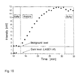
- Figure 18 shows the signal of one assay measured in this experiment.
- the curve starts at 10 minutes total time. By this time, everything was correctly prepared and adjusted.
- the first data points have been measured while buffer was flowing through the flow cell 5.
- This is the background level that originates from scattered laser light and from the volume fluorescence of the polycarbonate substrate S.
- the shutter blocking the laser was opened for 5 seconds once per minute. The level measured during the time the shutter was closed corresponds to the photomultiplier dark counts.
- the reagent present in a concentration of 10 -8 M in the same buffer solution, was applied to the flow cell.
- the rise of the sensor output signal between times 13 and 28 is due to the absorption of antibodies, conjugated with Cy-5, to the mouse-IgG layer on the chip surface.
- the intensity corresponds to the fluorescent light emitted by the Cy-5-label of these molecules into the TE 0 waveguide mode. After about 15 minutes (minute 28) the signal rise ended. This effect shows that the antibodies saturated the binding sites on the surface. The signal diminished a little after buffer was applied on the chip again (minute 31). This small decrease corresponds to the former contribution to the signal by those molecules which were only unspecifically absorbed and/or just present in the analyte volume in the region of the evanescent wave and non washed away.
- Figures 19-23 show calculations illustrating the advantages of the sensor according to the invention. The following definitions are used:
- Figure 19 shows the excitation (dashed line) and emission (solid line) angles (in degrees) for a conventional waveguide sensor using
- the angular separation between the background contribution and the signal is in the order of 3°.
- Figure 20 shows the excitation (dashed line) and emission (solid line) angles (in degrees) for a waveguide sensor according to the invention using
- the angular separation is larger than about 9°, and still leaves a great freedom for designing the absolute angles for optimizing readout; choosing a periodicity of 330 nm leads for instance to an output angle near 0° (i.e. normal to the surface).
- the separation can be further increased by choosing a greater periodicity, reaching values of more than 20° (e.g. at ⁇ > 600 nm).
- An additional advantage of this approach is that the background suppression can be further enhanced by using polarization filters in the output channel.
- Figure 21 shows the excitation (dashed line) and emission (solid line) angles (in degrees) for a waveguide sensor according to the invention using
- the angular separation is larger than 30°, and still leaves a great freedom for designing the absolute angles for optimizing readout; choosing a periodicity of 400 nm leads for instance to an output angle near 0° (i.e. normal to the surface).
- the separation can be further increased by choosing a greater periodicity, reaching values of more than 40° (e.g. at ⁇ > 480 nm).
- Figure 22 shows the excitation (dashed line) and emission (solid line) angles (in degrees) for a waveguide sensor according to the invention using
- the angular separation is larger than 70°, however, the freedom for designing the absolute angles for optimizing readout is somewhat limited, but still allows low angles if large grating periodicities are chosen; choosing a periodicity of > 600 nm leads for instance to output angles of a magnitude less than about 20° away from normal incidence.
- the separation can be further increased by choosing a periodicity in the vicinity of 580 nm, reaching values of about 100°.
- Figure 23 shows the excitation (dashed line) and emission (solid line) angles (in degrees) for a waveguide sensor according to the invention using
- the angular separation is larger than 60°, and still allows low angles if large grating periodicities are chosen; choosing a periodicity of > 600 nm leads for instance to output angles of a magnitude less than about 10° degrees away from normal incidence.
- polarization filters leads to additional improvements in this example.
Landscapes
- Health & Medical Sciences (AREA)
- Chemical & Material Sciences (AREA)
- Physics & Mathematics (AREA)
- Immunology (AREA)
- Pathology (AREA)
- Biochemistry (AREA)
- General Health & Medical Sciences (AREA)
- General Physics & Mathematics (AREA)
- Life Sciences & Earth Sciences (AREA)
- Analytical Chemistry (AREA)
- Chemical Kinetics & Catalysis (AREA)
- Nuclear Medicine, Radiotherapy & Molecular Imaging (AREA)
- Engineering & Computer Science (AREA)
- Plasma & Fusion (AREA)
- Optics & Photonics (AREA)
- Investigating, Analyzing Materials By Fluorescence Or Luminescence (AREA)
- Glass Compositions (AREA)
- Investigating Or Analyzing Materials By The Use Of Electric Means (AREA)
- Investigating Or Analysing Materials By The Use Of Chemical Reactions (AREA)
- Investigating Or Analysing Materials By Optical Means (AREA)
Priority Applications (4)
| Application Number | Priority Date | Filing Date | Title |
|---|---|---|---|
| AT99118309T ATE244883T1 (de) | 1999-09-15 | 1999-09-15 | Integriert-optischer sensor |
| DE69909480T DE69909480T2 (de) | 1999-09-15 | 1999-09-15 | Integriert-optischer Sensor |
| EP99118309A EP1085315B1 (de) | 1999-09-15 | 1999-09-15 | Integriert-optischer Sensor |
| US09/660,978 US6483096B1 (en) | 1999-09-15 | 2000-09-13 | Integrated-optical chemical and biochemical sensor |
Applications Claiming Priority (1)
| Application Number | Priority Date | Filing Date | Title |
|---|---|---|---|
| EP99118309A EP1085315B1 (de) | 1999-09-15 | 1999-09-15 | Integriert-optischer Sensor |
Publications (2)
| Publication Number | Publication Date |
|---|---|
| EP1085315A1 true EP1085315A1 (de) | 2001-03-21 |
| EP1085315B1 EP1085315B1 (de) | 2003-07-09 |
Family
ID=8239010
Family Applications (1)
| Application Number | Title | Priority Date | Filing Date |
|---|---|---|---|
| EP99118309A Expired - Lifetime EP1085315B1 (de) | 1999-09-15 | 1999-09-15 | Integriert-optischer Sensor |
Country Status (4)
| Country | Link |
|---|---|
| US (1) | US6483096B1 (de) |
| EP (1) | EP1085315B1 (de) |
| AT (1) | ATE244883T1 (de) |
| DE (1) | DE69909480T2 (de) |
Cited By (20)
| Publication number | Priority date | Publication date | Assignee | Title |
|---|---|---|---|---|
| FR2813121A1 (fr) * | 2000-08-21 | 2002-02-22 | Claude Weisbuch | Dispositif perfectionne de support d'elements chromophores |
| WO2004020985A1 (en) * | 2002-09-02 | 2004-03-11 | Medical Biosystems Ltd. | Biosensor |
| EP1468291A1 (de) * | 2002-01-28 | 2004-10-20 | Sru Biosystems, LLC | Label-freie optische technik mit hohem durchsatz zur erkennung von biomolekularen wechselwirkungen |
| EP1622200A1 (de) * | 2004-07-26 | 2006-02-01 | CSEM Centre Suisse d'Electronique et de Microtechnique SA | Festkörper-Fotodetektor-Pixel und Fotodetektionsverfahren |
| EP1653222A1 (de) * | 2004-11-01 | 2006-05-03 | Terumo Kabushiki Kaisha | Lichtwellenleiter und Fluoreszenzsensor mit dem Lichtwellenleiter |
| WO2007010469A1 (en) | 2005-07-21 | 2007-01-25 | Koninklijke Philips Electronics N. V. | Device for detection of excitation using a multiple spot arrangement |
| EP1752793A1 (de) | 2005-08-08 | 2007-02-14 | CSEM Centre Suisse d'Electronique et de Microtechnique SA | Verfahren und Vorrichtung für redundante Abstandsmessung und für das Aufheben von Phasenversatz |
| EP1788036A1 (de) * | 2005-11-16 | 2007-05-23 | CSEM Centre Suisse d'Electronique et de Microtechnique SA Recherche et Développement | Verfahren zur Herstellung von J-Aggregaten |
| WO2007091280A1 (en) * | 2006-02-06 | 2007-08-16 | Stmicroelectronics S.R.L. | Optical apparatus and method for the inspection of nucleic acid probes by polarized radiation |
| DE102007033124A1 (de) * | 2007-07-16 | 2009-01-22 | Fraunhofer-Gesellschaft zur Förderung der angewandten Forschung e.V. | Vorrichtung zur optischen Detektion von Substanzen in einem flüssigen oder gasförmigen Medium |
| US8111401B2 (en) | 1999-11-05 | 2012-02-07 | Robert Magnusson | Guided-mode resonance sensors employing angular, spectral, modal, and polarization diversity for high-precision sensing in compact formats |
| WO2012018364A1 (en) * | 2010-07-08 | 2012-02-09 | The Board Of Trustees Of The University Of Illinois | Multi-color fluorescence enhancement from a photonic crystal surface |
| US8293542B2 (en) | 2000-10-30 | 2012-10-23 | X-Body, Inc. | Real time binding analysis of antigens on a biosensor surface |
| EP2824446A1 (de) * | 2013-07-12 | 2015-01-14 | F. Hoffmann-La Roche AG | Vorrichtung zur Verwendung bei der Bindeaffinitätserkennung |
| EP2884261A1 (de) * | 2013-12-14 | 2015-06-17 | IMEC vzw | Integrierte Fluoreszenzdetektion |
| CN104937417A (zh) * | 2013-01-17 | 2015-09-23 | 弗·哈夫曼-拉罗切有限公司 | 用于制备能够沿多个预定线条来结合目标样本的平面波导的外表面的方法以及平面波导 |
| WO2016055527A3 (en) * | 2014-10-09 | 2016-06-09 | Aston University | Optical detector module, measurement system and method of detecting presence of a substance in a test material |
| US9778267B2 (en) | 2007-07-11 | 2017-10-03 | X-Body, Inc. | Methods for identifying modulators of ion channels |
| US10359573B2 (en) | 1999-11-05 | 2019-07-23 | Board Of Regents, The University Of Texas System | Resonant waveguide-granting devices and methods for using same |
| US11016100B2 (en) | 2007-07-11 | 2021-05-25 | X-Body, Inc. | Methods for identifying modulators of ion channels |
Families Citing this family (52)
| Publication number | Priority date | Publication date | Assignee | Title |
|---|---|---|---|---|
| AU2001281632A1 (en) | 2000-08-09 | 2002-02-18 | Artificial Sensing Instruments Asi Ag | Waveguide grid array and optical measurement arrangement |
| US7118710B2 (en) | 2000-10-30 | 2006-10-10 | Sru Biosystems, Inc. | Label-free high-throughput optical technique for detecting biomolecular interactions |
| US7875434B2 (en) | 2000-10-30 | 2011-01-25 | Sru Biosystems, Inc. | Label-free methods for performing assays using a colorimetric resonant reflectance optical biosensor |
| US7575939B2 (en) | 2000-10-30 | 2009-08-18 | Sru Biosystems, Inc. | Optical detection of label-free biomolecular interactions using microreplicated plastic sensor elements |
| US7371562B2 (en) | 2000-10-30 | 2008-05-13 | Sru Biosystems, Inc. | Guided mode resonant filter biosensor using a linear grating surface structure |
| US6707958B2 (en) * | 2001-11-20 | 2004-03-16 | Agilent Technologies, Inc. | Biochemical assay device using frustrated total internal reflection modulator with an imaging optical waveguide |
| US7927822B2 (en) | 2002-09-09 | 2011-04-19 | Sru Biosystems, Inc. | Methods for screening cells and antibodies |
| US7492978B2 (en) * | 2002-10-07 | 2009-02-17 | The Secretary Of State For Defence | Waveguide structure |
| US7309614B1 (en) | 2002-12-04 | 2007-12-18 | Sru Biosystems, Inc. | Self-referencing biodetection method and patterned bioassays |
| US7027163B2 (en) * | 2003-01-24 | 2006-04-11 | General Dynamics Advanced Information Systems, Inc. | Grating sensor |
| US20050018944A1 (en) * | 2003-07-25 | 2005-01-27 | Mozdy Eric J. | Polarization modulation interrogation of grating-coupled waveguide sensors |
| US8298780B2 (en) | 2003-09-22 | 2012-10-30 | X-Body, Inc. | Methods of detection of changes in cells |
| KR100543705B1 (ko) * | 2003-11-20 | 2006-01-20 | 삼성전자주식회사 | 2차원적 격자가 형성되어 있는 기판을 포함하는 마이크로 어레이 및 그를 이용하는 표적 분자의 검출방법 |
| KR100580631B1 (ko) * | 2003-11-22 | 2006-05-16 | 삼성전자주식회사 | 산화막을 갖는 기판, 그를 이용한 표적 물질 검출 방법 및광학적 센서 |
| KR100590548B1 (ko) * | 2004-03-03 | 2006-06-19 | 삼성전자주식회사 | 광검출 장치 |
| KR100634505B1 (ko) * | 2004-06-16 | 2006-10-16 | 삼성전자주식회사 | 패턴화된 박막층을 갖는 마이크로어레이 기판 및마이크로어레이, 상기 마이크로어레이 기판 및마이크로어레이를 제조하는 방법 |
| FR2873445A1 (fr) * | 2004-07-26 | 2006-01-27 | Genewave Soc Par Actions Simpl | Dispositif de detection de la fluorescence emise par des elements chromophores dans des puits d'une plaque a puits multiples |
| US7709247B2 (en) * | 2004-08-04 | 2010-05-04 | Intel Corporation | Methods and systems for detecting biomolecular binding using terahertz radiation |
| EP1938049B1 (de) * | 2005-09-22 | 2019-01-02 | Koninklijke Philips N.V. | Lumineszenzsensor mit mindestens zwei drahtgittern |
| TWI296044B (en) * | 2005-11-03 | 2008-04-21 | Ind Tech Res Inst | Coupled waveguide-surface plasmon resonance biosensor |
| TWI312414B (en) * | 2005-12-16 | 2009-07-21 | Ind Tech Res Inst | Optic waveguide biiosensing device |
| US9528939B2 (en) | 2006-03-10 | 2016-12-27 | Indx Lifecare, Inc. | Waveguide-based optical scanning systems |
| US8288157B2 (en) | 2007-09-12 | 2012-10-16 | Plc Diagnostics, Inc. | Waveguide-based optical scanning systems |
| US9976192B2 (en) | 2006-03-10 | 2018-05-22 | Ldip, Llc | Waveguide-based detection system with scanning light source |
| US7951583B2 (en) | 2006-03-10 | 2011-05-31 | Plc Diagnostics, Inc. | Optical scanning system |
| US9423397B2 (en) | 2006-03-10 | 2016-08-23 | Indx Lifecare, Inc. | Waveguide-based detection system with scanning light source |
| CN101595380B (zh) * | 2006-10-31 | 2012-10-24 | 皇家飞利浦电子股份有限公司 | 使用线栅增加腔体能量的生物传感器 |
| WO2009107041A1 (en) * | 2008-02-25 | 2009-09-03 | Koninklijke Philips Electronics N.V. | Optical sensor for measuring emission light from an analyte |
| US8257936B2 (en) | 2008-04-09 | 2012-09-04 | X-Body Inc. | High resolution label free analysis of cellular properties |
| EP2110694B1 (de) * | 2008-04-18 | 2013-08-14 | Sony DADC Austria AG | Verfahren zur Herstellung eines optischen Wellenleiters, optischer Wellenleiter und Sensoranordnung |
| GB2461026B (en) | 2008-06-16 | 2011-03-09 | Plc Diagnostics Inc | System and method for nucleic acids sequencing by phased synthesis |
| US8258450B1 (en) * | 2008-06-26 | 2012-09-04 | University Of South Florida | Physical and chemical integrated flow imaging device |
| EP3572796B8 (de) | 2008-10-27 | 2023-01-18 | Genalyte, Inc. | Biosensoren basierend auf optischer sondierung und abtastung |
| CA2759396A1 (en) | 2009-04-29 | 2010-11-04 | Plc Diagnostics Inc. | Waveguide-based detection system with scanning light source |
| US8994946B2 (en) | 2010-02-19 | 2015-03-31 | Pacific Biosciences Of California, Inc. | Integrated analytical system and method |
| EP2933629B1 (de) | 2010-02-19 | 2019-04-10 | Pacific Biosciences Of California, Inc. | System zur Messung von analytischen Reaktionen umfassend eine Buchse für einen Optode-Arraychip |
| US9726871B2 (en) | 2013-02-01 | 2017-08-08 | Bio-Rad Laboratories, Inc. | Detection system with one-piece optical element to concentrate and homogenize light |
| EP2827130A1 (de) * | 2013-07-15 | 2015-01-21 | F. Hoffmann-La Roche AG | Vorrichtung zur Verwendung bei der Bindeaffinitätserkennung |
| US9410893B2 (en) | 2013-11-22 | 2016-08-09 | Taiwan Semiconductor Manufacturing Company, Ltd. | Bio-chip package with waveguide integrated spectrometer |
| EP3087421B1 (de) * | 2013-12-23 | 2019-07-31 | CSEM Centre Suisse d'Electronique et de Microtechnique SA - Recherche et Développement | Wellenleitergittervorrichtung |
| US10018566B2 (en) | 2014-02-28 | 2018-07-10 | Ldip, Llc | Partially encapsulated waveguide based sensing chips, systems and methods of use |
| US11181479B2 (en) | 2015-02-27 | 2021-11-23 | Ldip, Llc | Waveguide-based detection system with scanning light source |
| JP6569856B2 (ja) * | 2015-03-13 | 2019-09-04 | パナソニックIpマネジメント株式会社 | 発光装置および内視鏡 |
| AU2016259012C1 (en) | 2015-05-07 | 2022-11-17 | Pacific Biosciences Of California, Inc. | Multiprocessor pipeline architecture |
| US10359155B2 (en) | 2015-08-20 | 2019-07-23 | Panasonic Intellectual Property Management Co., Ltd. | Light-emitting apparatus |
| CN111066263B (zh) * | 2017-07-21 | 2023-10-03 | 加州理工学院 | 超薄平面无透镜相机 |
| WO2019033110A1 (en) | 2017-08-11 | 2019-02-14 | California Institute Of Technology | THIN-DIMENSIONAL IMAGING WITHOUT LENS USING DIRECTIONAL DETECTION ELEMENTS |
| EP3492909B1 (de) * | 2017-12-01 | 2023-11-01 | ams AG | Chemische erfassungsvorrichtung mit fluoreszierendem sensormaterial |
| TWI683085B (zh) | 2018-10-12 | 2020-01-21 | 國立交通大學 | 光學位移感測系統 |
| TWI687676B (zh) * | 2019-04-29 | 2020-03-11 | 國立中正大學 | 生物感測器自我補償系統 |
| US11406977B2 (en) * | 2019-06-28 | 2022-08-09 | Illumina Cambridge Limited | Flowcells with linear waveguides |
| DE102021112256A1 (de) | 2020-12-29 | 2022-06-30 | Interherence GmbH | Opto-elektronischer Chip |
Citations (1)
| Publication number | Priority date | Publication date | Assignee | Title |
|---|---|---|---|---|
| WO1997037211A1 (de) * | 1996-03-30 | 1997-10-09 | Novartis Ag | Integriert optischer lumineszenzsensor |
Family Cites Families (2)
| Publication number | Priority date | Publication date | Assignee | Title |
|---|---|---|---|---|
| GB8807486D0 (en) * | 1988-03-29 | 1988-05-05 | Ares Serono Res & Dev Ltd | Waveguide sensor |
| FR2778986B1 (fr) * | 1998-05-22 | 2000-07-21 | Suisse Electronique Microtech | Capteur optique utilisant une reaction immunologique et un marqueur fluorescent |
-
1999
- 1999-09-15 DE DE69909480T patent/DE69909480T2/de not_active Expired - Fee Related
- 1999-09-15 AT AT99118309T patent/ATE244883T1/de not_active IP Right Cessation
- 1999-09-15 EP EP99118309A patent/EP1085315B1/de not_active Expired - Lifetime
-
2000
- 2000-09-13 US US09/660,978 patent/US6483096B1/en not_active Expired - Fee Related
Patent Citations (1)
| Publication number | Priority date | Publication date | Assignee | Title |
|---|---|---|---|---|
| WO1997037211A1 (de) * | 1996-03-30 | 1997-10-09 | Novartis Ag | Integriert optischer lumineszenzsensor |
Non-Patent Citations (2)
| Title |
|---|
| DESSY R E: "Waveguides as chemical sensors", ANALYTICAL CHEMISTRY, vol. 61, no. 19, October 1989 (1989-10-01), ISSN 0003-2700, pages 1079A-1094A, XP000088109 * |
| KUNZ R E: "Miniature integrated optical modules for chemical and biochemical sensing", SENSORS AND ACTUATORS B, vol. B38, no. 1-3, February 1997 (1997-02-01), ISSN 0925-4005, pages 13-28, XP004083666 * |
Cited By (42)
| Publication number | Priority date | Publication date | Assignee | Title |
|---|---|---|---|---|
| US8111401B2 (en) | 1999-11-05 | 2012-02-07 | Robert Magnusson | Guided-mode resonance sensors employing angular, spectral, modal, and polarization diversity for high-precision sensing in compact formats |
| US10359573B2 (en) | 1999-11-05 | 2019-07-23 | Board Of Regents, The University Of Texas System | Resonant waveguide-granting devices and methods for using same |
| FR2813121A1 (fr) * | 2000-08-21 | 2002-02-22 | Claude Weisbuch | Dispositif perfectionne de support d'elements chromophores |
| WO2002016912A1 (fr) * | 2000-08-21 | 2002-02-28 | Genewave | Dispositif de support d'elements chromophores |
| US6867900B2 (en) | 2000-08-21 | 2005-03-15 | Genewave | Support for chromophoric elements |
| US8293542B2 (en) | 2000-10-30 | 2012-10-23 | X-Body, Inc. | Real time binding analysis of antigens on a biosensor surface |
| EP1468291A1 (de) * | 2002-01-28 | 2004-10-20 | Sru Biosystems, LLC | Label-freie optische technik mit hohem durchsatz zur erkennung von biomolekularen wechselwirkungen |
| EP1468291A4 (de) * | 2002-01-28 | 2010-04-14 | Sru Biosystems Inc | Label-freie optische technik mit hohem durchsatz zur erkennung von biomolekularen wechselwirkungen |
| WO2004020985A1 (en) * | 2002-09-02 | 2004-03-11 | Medical Biosystems Ltd. | Biosensor |
| US9209327B2 (en) | 2004-07-26 | 2015-12-08 | Heptagon Micro Optics Pte. Ltd. | Solid-state photodetector pixel and photodetecting method |
| US7897928B2 (en) | 2004-07-26 | 2011-03-01 | Mesa Imaging Ag | Solid-state photodetector pixel and photodetecting method |
| EP1622200A1 (de) * | 2004-07-26 | 2006-02-01 | CSEM Centre Suisse d'Electronique et de Microtechnique SA | Festkörper-Fotodetektor-Pixel und Fotodetektionsverfahren |
| US7181096B2 (en) | 2004-11-01 | 2007-02-20 | Terumo Kabushiki Kaisha | Light waveguide and fluorescent sensor using the light waveguide |
| EP1653222A1 (de) * | 2004-11-01 | 2006-05-03 | Terumo Kabushiki Kaisha | Lichtwellenleiter und Fluoreszenzsensor mit dem Lichtwellenleiter |
| WO2007010469A1 (en) | 2005-07-21 | 2007-01-25 | Koninklijke Philips Electronics N. V. | Device for detection of excitation using a multiple spot arrangement |
| EP1910809A1 (de) * | 2005-07-21 | 2008-04-16 | Koninklijke Philips Electronics N.V. | Vorrichtung zur erkennung von erregung mithilfe einer multiplen punktanordnung |
| EP1752793A1 (de) | 2005-08-08 | 2007-02-14 | CSEM Centre Suisse d'Electronique et de Microtechnique SA | Verfahren und Vorrichtung für redundante Abstandsmessung und für das Aufheben von Phasenversatz |
| US7462808B2 (en) | 2005-08-08 | 2008-12-09 | Mesa Imaging Ag | Method and device for redundant distance measurement and mismatch cancellation in phase-measurement systems |
| EP1788036A1 (de) * | 2005-11-16 | 2007-05-23 | CSEM Centre Suisse d'Electronique et de Microtechnique SA Recherche et Développement | Verfahren zur Herstellung von J-Aggregaten |
| WO2007057356A3 (fr) * | 2005-11-16 | 2007-08-23 | Suisse Electronique Microtech | Procede de realisation d'agregats j |
| WO2007057356A2 (fr) * | 2005-11-16 | 2007-05-24 | Csem Centre Suisse D'electronique Et De Microtechnique Sa Recherche Et Developpement | Procede de realisation d'agregats j |
| US8088929B2 (en) | 2005-11-16 | 2012-01-03 | Csem Centre Suisse D'electronique Et De Microtechnique Sa - Recherche Et Developpment | Method for producing J aggregates |
| WO2007091280A1 (en) * | 2006-02-06 | 2007-08-16 | Stmicroelectronics S.R.L. | Optical apparatus and method for the inspection of nucleic acid probes by polarized radiation |
| US11016100B2 (en) | 2007-07-11 | 2021-05-25 | X-Body, Inc. | Methods for identifying modulators of ion channels |
| US9778267B2 (en) | 2007-07-11 | 2017-10-03 | X-Body, Inc. | Methods for identifying modulators of ion channels |
| DE102007033124A1 (de) * | 2007-07-16 | 2009-01-22 | Fraunhofer-Gesellschaft zur Förderung der angewandten Forschung e.V. | Vorrichtung zur optischen Detektion von Substanzen in einem flüssigen oder gasförmigen Medium |
| DE102007033124B4 (de) * | 2007-07-16 | 2012-12-06 | Fraunhofer-Gesellschaft zur Förderung der angewandten Forschung e.V. | Vorrichtung zur optischen Detektion von Substanzen in einem flüssigen oder gasförmigen Medium |
| US8877129B2 (en) | 2007-07-16 | 2014-11-04 | Fraunhofer-Gesellschaft Zur Foerderung Der Angewandten Forschung E.V. | Method and device for optical detection of substances in a liquid or gaseous medium |
| WO2012018364A1 (en) * | 2010-07-08 | 2012-02-09 | The Board Of Trustees Of The University Of Illinois | Multi-color fluorescence enhancement from a photonic crystal surface |
| US8344333B2 (en) | 2010-07-08 | 2013-01-01 | The Board Of Trustees Of The University Of Illinois | Multi-color fluorescence enhancement from a photonic crystal surface |
| CN104937417A (zh) * | 2013-01-17 | 2015-09-23 | 弗·哈夫曼-拉罗切有限公司 | 用于制备能够沿多个预定线条来结合目标样本的平面波导的外表面的方法以及平面波导 |
| CN104937417B (zh) * | 2013-01-17 | 2017-05-17 | 弗·哈夫曼-拉罗切有限公司 | 用于制备能够沿多个预定线条来结合目标样本的平面波导的外表面的方法以及平面波导 |
| CN105378463A (zh) * | 2013-07-12 | 2016-03-02 | 弗·哈夫曼-拉罗切有限公司 | 用于检测结合亲和力的装置 |
| JP2016524163A (ja) * | 2013-07-12 | 2016-08-12 | エフ.ホフマン−ラ ロッシュ アーゲー | 結合親和性の検出に用いる装置 |
| US10060917B2 (en) | 2013-07-12 | 2018-08-28 | Hoffmann-La Roche Inc. | Device for use in the detection of binding affinities |
| CN105378463B (zh) * | 2013-07-12 | 2019-07-05 | 弗·哈夫曼-拉罗切有限公司 | 用于检测结合亲和力的装置 |
| WO2015004264A1 (en) * | 2013-07-12 | 2015-01-15 | F. Hoffmann-La Roche Ag | Device for use in the detection of binding affinities |
| EP2824446A1 (de) * | 2013-07-12 | 2015-01-14 | F. Hoffmann-La Roche AG | Vorrichtung zur Verwendung bei der Bindeaffinitätserkennung |
| US9146235B2 (en) | 2013-12-14 | 2015-09-29 | Imec Vzw | Integrated fluorescence detection |
| EP2884261A1 (de) * | 2013-12-14 | 2015-06-17 | IMEC vzw | Integrierte Fluoreszenzdetektion |
| WO2016055527A3 (en) * | 2014-10-09 | 2016-06-09 | Aston University | Optical detector module, measurement system and method of detecting presence of a substance in a test material |
| US9976950B2 (en) | 2014-10-09 | 2018-05-22 | Aston University | Optical detector module, measurement system and method of detecting presence of a substance in a test material |
Also Published As
| Publication number | Publication date |
|---|---|
| EP1085315B1 (de) | 2003-07-09 |
| US6483096B1 (en) | 2002-11-19 |
| DE69909480T2 (de) | 2004-04-15 |
| DE69909480D1 (de) | 2003-08-14 |
| ATE244883T1 (de) | 2003-07-15 |
Similar Documents
| Publication | Publication Date | Title |
|---|---|---|
| US6483096B1 (en) | Integrated-optical chemical and biochemical sensor | |
| JP3645907B2 (ja) | 漸減励起された発光を検出する方法 | |
| EP1078248B1 (de) | Optische sensorvorrichtung mit evaneszenter felddetektion | |
| KR100696237B1 (ko) | 통합형 다중-도파관 센서 | |
| US6395558B1 (en) | Optical chemical/biochemical sensor | |
| Duveneck et al. | Novel bioaffinity sensors for trace analysis based on luminescence excitation by planar waveguides | |
| CA1314743C (en) | Waveguide sensor | |
| US20040046128A1 (en) | Sensor platform and method for the determination of multiple analytes | |
| EP2916125A1 (de) | Fluoreszenz-Assays auf mikrofluidischen Chips | |
| EP1938049B1 (de) | Lumineszenzsensor mit mindestens zwei drahtgittern | |
| JP2011503536A (ja) | マイクロエレクトロニクスセンサ | |
| EP2962086B1 (de) | Probenplatte und analyseverfahren | |
| JP2007286045A (ja) | 検出装置、検出素子用基板、検出素子、検出素子用キット及び検出方法 | |
| EP0382832B1 (de) | Testverfahren fuer einen in einer probe enthaltenden ligand | |
| CN102985804A (zh) | 具有大规模制造设计的盒 | |
| CN103930765A (zh) | 用于团簇检测的装置 | |
| US9891171B2 (en) | Sensing module and sensing method | |
| JP2009192259A (ja) | センシング装置 | |
| US20120181451A1 (en) | Waveguide-based Sensor | |
| Christensen et al. | Optical immunoassay systems based upon evanescent wave interactions | |
| Ives et al. | Total internal reflection fluorescence surface sensors | |
| KR20060089103A (ko) | 구형 공진기를 이용한 바이오칩 플랫폼 및 이를 구비하는생체시료 검출 소자 | |
| Hua | Integrated optical fluorescence multi-sensor system | |
| Kolari et al. | Optimising a grating-coupled evanescent field excitation |
Legal Events
| Date | Code | Title | Description |
|---|---|---|---|
| PUAI | Public reference made under article 153(3) epc to a published international application that has entered the european phase |
Free format text: ORIGINAL CODE: 0009012 |
|
| AK | Designated contracting states |
Kind code of ref document: A1 Designated state(s): AT BE CH CY DE DK ES FI FR GB GR IE IT LI LU MC NL PT SE |
|
| AX | Request for extension of the european patent |
Free format text: AL;LT;LV;MK;RO;SI |
|
| 17P | Request for examination filed |
Effective date: 20010602 |
|
| 17Q | First examination report despatched |
Effective date: 20011004 |
|
| AKX | Designation fees paid |
Free format text: AT BE CH CY DE DK ES FI FR GB GR IE IT LI LU MC NL PT SE |
|
| GRAH | Despatch of communication of intention to grant a patent |
Free format text: ORIGINAL CODE: EPIDOS IGRA |
|
| GRAH | Despatch of communication of intention to grant a patent |
Free format text: ORIGINAL CODE: EPIDOS IGRA |
|
| GRAA | (expected) grant |
Free format text: ORIGINAL CODE: 0009210 |
|
| AK | Designated contracting states |
Designated state(s): AT BE CH CY DE DK ES FI FR GB GR IE IT LI LU MC NL PT SE |
|
| PG25 | Lapsed in a contracting state [announced via postgrant information from national office to epo] |
Ref country code: NL Free format text: LAPSE BECAUSE OF FAILURE TO SUBMIT A TRANSLATION OF THE DESCRIPTION OR TO PAY THE FEE WITHIN THE PRESCRIBED TIME-LIMIT Effective date: 20030709 Ref country code: IT Free format text: LAPSE BECAUSE OF FAILURE TO SUBMIT A TRANSLATION OF THE DESCRIPTION OR TO PAY THE FEE WITHIN THE PRESCRIBED TIME-LIMIT;WARNING: LAPSES OF ITALIAN PATENTS WITH EFFECTIVE DATE BEFORE 2007 MAY HAVE OCCURRED AT ANY TIME BEFORE 2007. THE CORRECT EFFECTIVE DATE MAY BE DIFFERENT FROM THE ONE RECORDED. Effective date: 20030709 Ref country code: FI Free format text: LAPSE BECAUSE OF FAILURE TO SUBMIT A TRANSLATION OF THE DESCRIPTION OR TO PAY THE FEE WITHIN THE PRESCRIBED TIME-LIMIT Effective date: 20030709 Ref country code: BE Free format text: LAPSE BECAUSE OF FAILURE TO SUBMIT A TRANSLATION OF THE DESCRIPTION OR TO PAY THE FEE WITHIN THE PRESCRIBED TIME-LIMIT Effective date: 20030709 Ref country code: AT Free format text: LAPSE BECAUSE OF FAILURE TO SUBMIT A TRANSLATION OF THE DESCRIPTION OR TO PAY THE FEE WITHIN THE PRESCRIBED TIME-LIMIT Effective date: 20030709 |
|
| REG | Reference to a national code |
Ref country code: GB Ref legal event code: FG4D |
|
| REG | Reference to a national code |
Ref country code: CH Ref legal event code: EP |
|
| REF | Corresponds to: |
Ref document number: 69909480 Country of ref document: DE Date of ref document: 20030814 Kind code of ref document: P |
|
| REG | Reference to a national code |
Ref country code: IE Ref legal event code: FG4D |
|
| PG25 | Lapsed in a contracting state [announced via postgrant information from national office to epo] |
Ref country code: LU Free format text: LAPSE BECAUSE OF NON-PAYMENT OF DUE FEES Effective date: 20030915 Ref country code: IE Free format text: LAPSE BECAUSE OF NON-PAYMENT OF DUE FEES Effective date: 20030915 Ref country code: CY Free format text: LAPSE BECAUSE OF FAILURE TO SUBMIT A TRANSLATION OF THE DESCRIPTION OR TO PAY THE FEE WITHIN THE PRESCRIBED TIME-LIMIT Effective date: 20030915 |
|
| PG25 | Lapsed in a contracting state [announced via postgrant information from national office to epo] |
Ref country code: MC Free format text: LAPSE BECAUSE OF NON-PAYMENT OF DUE FEES Effective date: 20030930 |
|
| PG25 | Lapsed in a contracting state [announced via postgrant information from national office to epo] |
Ref country code: SE Free format text: LAPSE BECAUSE OF FAILURE TO SUBMIT A TRANSLATION OF THE DESCRIPTION OR TO PAY THE FEE WITHIN THE PRESCRIBED TIME-LIMIT Effective date: 20031009 Ref country code: GR Free format text: LAPSE BECAUSE OF FAILURE TO SUBMIT A TRANSLATION OF THE DESCRIPTION OR TO PAY THE FEE WITHIN THE PRESCRIBED TIME-LIMIT Effective date: 20031009 Ref country code: DK Free format text: LAPSE BECAUSE OF FAILURE TO SUBMIT A TRANSLATION OF THE DESCRIPTION OR TO PAY THE FEE WITHIN THE PRESCRIBED TIME-LIMIT Effective date: 20031009 |
|
| REG | Reference to a national code |
Ref country code: CH Ref legal event code: NV Representative=s name: PATENTANWAELTE FELDMANN & PARTNER AG |
|
| PG25 | Lapsed in a contracting state [announced via postgrant information from national office to epo] |
Ref country code: ES Free format text: LAPSE BECAUSE OF FAILURE TO SUBMIT A TRANSLATION OF THE DESCRIPTION OR TO PAY THE FEE WITHIN THE PRESCRIBED TIME-LIMIT Effective date: 20031020 |
|
| NLV1 | Nl: lapsed or annulled due to failure to fulfill the requirements of art. 29p and 29m of the patents act | ||
| PG25 | Lapsed in a contracting state [announced via postgrant information from national office to epo] |
Ref country code: PT Free format text: LAPSE BECAUSE OF FAILURE TO SUBMIT A TRANSLATION OF THE DESCRIPTION OR TO PAY THE FEE WITHIN THE PRESCRIBED TIME-LIMIT Effective date: 20031209 |
|
| PLBE | No opposition filed within time limit |
Free format text: ORIGINAL CODE: 0009261 |
|
| STAA | Information on the status of an ep patent application or granted ep patent |
Free format text: STATUS: NO OPPOSITION FILED WITHIN TIME LIMIT |
|
| ET | Fr: translation filed | ||
| 26N | No opposition filed |
Effective date: 20040414 |
|
| REG | Reference to a national code |
Ref country code: IE Ref legal event code: MM4A |
|
| PGFP | Annual fee paid to national office [announced via postgrant information from national office to epo] |
Ref country code: FR Payment date: 20080912 Year of fee payment: 10 |
|
| PGFP | Annual fee paid to national office [announced via postgrant information from national office to epo] |
Ref country code: GB Payment date: 20080918 Year of fee payment: 10 |
|
| PGFP | Annual fee paid to national office [announced via postgrant information from national office to epo] |
Ref country code: DE Payment date: 20080919 Year of fee payment: 10 |
|
| REG | Reference to a national code |
Ref country code: GB Ref legal event code: S117 Free format text: REQUEST FILED; REQUEST FOR CORRECTION UNDER SECTION 117 FILED ON 12 JUNE 2009 |
|
| REG | Reference to a national code |
Ref country code: GB Ref legal event code: S117 Free format text: CORRECTIONS ALLOWED |
|
| GBPC | Gb: european patent ceased through non-payment of renewal fee |
Effective date: 20090915 |
|
| REG | Reference to a national code |
Ref country code: FR Ref legal event code: ST Effective date: 20100531 |
|
| PG25 | Lapsed in a contracting state [announced via postgrant information from national office to epo] |
Ref country code: FR Free format text: LAPSE BECAUSE OF NON-PAYMENT OF DUE FEES Effective date: 20090930 Ref country code: DE Free format text: LAPSE BECAUSE OF NON-PAYMENT OF DUE FEES Effective date: 20100401 |
|
| PG25 | Lapsed in a contracting state [announced via postgrant information from national office to epo] |
Ref country code: GB Free format text: LAPSE BECAUSE OF NON-PAYMENT OF DUE FEES Effective date: 20090915 |
|
| PGFP | Annual fee paid to national office [announced via postgrant information from national office to epo] |
Ref country code: CH Payment date: 20141031 Year of fee payment: 16 |
|
| REG | Reference to a national code |
Ref country code: CH Ref legal event code: PL |
|
| PG25 | Lapsed in a contracting state [announced via postgrant information from national office to epo] |
Ref country code: CH Free format text: LAPSE BECAUSE OF NON-PAYMENT OF DUE FEES Effective date: 20150930 Ref country code: LI Free format text: LAPSE BECAUSE OF NON-PAYMENT OF DUE FEES Effective date: 20150930 |