EP1077591A2 - Vorschaltgerät für Starkstromgasentladungslampe - Google Patents
Vorschaltgerät für Starkstromgasentladungslampe Download PDFInfo
- Publication number
- EP1077591A2 EP1077591A2 EP00116154A EP00116154A EP1077591A2 EP 1077591 A2 EP1077591 A2 EP 1077591A2 EP 00116154 A EP00116154 A EP 00116154A EP 00116154 A EP00116154 A EP 00116154A EP 1077591 A2 EP1077591 A2 EP 1077591A2
- Authority
- EP
- European Patent Office
- Prior art keywords
- circuit
- lamp
- voltage
- inverter
- transformer
- Prior art date
- Legal status (The legal status is an assumption and is not a legal conclusion. Google has not performed a legal analysis and makes no representation as to the accuracy of the status listed.)
- Granted
Links
Images
Classifications
-
- H—ELECTRICITY
- H05—ELECTRIC TECHNIQUES NOT OTHERWISE PROVIDED FOR
- H05B—ELECTRIC HEATING; ELECTRIC LIGHT SOURCES NOT OTHERWISE PROVIDED FOR; CIRCUIT ARRANGEMENTS FOR ELECTRIC LIGHT SOURCES, IN GENERAL
- H05B41/00—Circuit arrangements or apparatus for igniting or operating discharge lamps
- H05B41/14—Circuit arrangements
- H05B41/26—Circuit arrangements in which the lamp is fed by power derived from DC by means of a converter, e.g. by high-voltage DC
- H05B41/28—Circuit arrangements in which the lamp is fed by power derived from DC by means of a converter, e.g. by high-voltage DC using static converters
- H05B41/288—Circuit arrangements in which the lamp is fed by power derived from DC by means of a converter, e.g. by high-voltage DC using static converters with semiconductor devices and specially adapted for lamps without preheating electrodes, e.g. for high-intensity discharge lamps, high-pressure mercury or sodium lamps or low-pressure sodium lamps
- H05B41/292—Arrangements for protecting lamps or circuits against abnormal operating conditions
- H05B41/2928—Arrangements for protecting lamps or circuits against abnormal operating conditions for protecting the lamp against abnormal operating conditions
-
- H—ELECTRICITY
- H05—ELECTRIC TECHNIQUES NOT OTHERWISE PROVIDED FOR
- H05B—ELECTRIC HEATING; ELECTRIC LIGHT SOURCES NOT OTHERWISE PROVIDED FOR; CIRCUIT ARRANGEMENTS FOR ELECTRIC LIGHT SOURCES, IN GENERAL
- H05B41/00—Circuit arrangements or apparatus for igniting or operating discharge lamps
- H05B41/14—Circuit arrangements
- H05B41/26—Circuit arrangements in which the lamp is fed by power derived from DC by means of a converter, e.g. by high-voltage DC
- H05B41/28—Circuit arrangements in which the lamp is fed by power derived from DC by means of a converter, e.g. by high-voltage DC using static converters
- H05B41/288—Circuit arrangements in which the lamp is fed by power derived from DC by means of a converter, e.g. by high-voltage DC using static converters with semiconductor devices and specially adapted for lamps without preheating electrodes, e.g. for high-intensity discharge lamps, high-pressure mercury or sodium lamps or low-pressure sodium lamps
- H05B41/2881—Load circuits; Control thereof
- H05B41/2882—Load circuits; Control thereof the control resulting from an action on the static converter
- H05B41/2883—Load circuits; Control thereof the control resulting from an action on the static converter the controlled element being a DC/AC converter in the final stage, e.g. by harmonic mode starting
-
- H—ELECTRICITY
- H05—ELECTRIC TECHNIQUES NOT OTHERWISE PROVIDED FOR
- H05B—ELECTRIC HEATING; ELECTRIC LIGHT SOURCES NOT OTHERWISE PROVIDED FOR; CIRCUIT ARRANGEMENTS FOR ELECTRIC LIGHT SOURCES, IN GENERAL
- H05B41/00—Circuit arrangements or apparatus for igniting or operating discharge lamps
- H05B41/14—Circuit arrangements
- H05B41/26—Circuit arrangements in which the lamp is fed by power derived from DC by means of a converter, e.g. by high-voltage DC
- H05B41/28—Circuit arrangements in which the lamp is fed by power derived from DC by means of a converter, e.g. by high-voltage DC using static converters
- H05B41/288—Circuit arrangements in which the lamp is fed by power derived from DC by means of a converter, e.g. by high-voltage DC using static converters with semiconductor devices and specially adapted for lamps without preheating electrodes, e.g. for high-intensity discharge lamps, high-pressure mercury or sodium lamps or low-pressure sodium lamps
- H05B41/2885—Static converters especially adapted therefor; Control thereof
- H05B41/2887—Static converters especially adapted therefor; Control thereof characterised by a controllable bridge in the final stage
-
- H—ELECTRICITY
- H05—ELECTRIC TECHNIQUES NOT OTHERWISE PROVIDED FOR
- H05B—ELECTRIC HEATING; ELECTRIC LIGHT SOURCES NOT OTHERWISE PROVIDED FOR; CIRCUIT ARRANGEMENTS FOR ELECTRIC LIGHT SOURCES, IN GENERAL
- H05B41/00—Circuit arrangements or apparatus for igniting or operating discharge lamps
- H05B41/14—Circuit arrangements
- H05B41/26—Circuit arrangements in which the lamp is fed by power derived from DC by means of a converter, e.g. by high-voltage DC
- H05B41/28—Circuit arrangements in which the lamp is fed by power derived from DC by means of a converter, e.g. by high-voltage DC using static converters
- H05B41/288—Circuit arrangements in which the lamp is fed by power derived from DC by means of a converter, e.g. by high-voltage DC using static converters with semiconductor devices and specially adapted for lamps without preheating electrodes, e.g. for high-intensity discharge lamps, high-pressure mercury or sodium lamps or low-pressure sodium lamps
- H05B41/292—Arrangements for protecting lamps or circuits against abnormal operating conditions
- H05B41/2921—Arrangements for protecting lamps or circuits against abnormal operating conditions for protecting the circuit against abnormal operating conditions
- H05B41/2925—Arrangements for protecting lamps or circuits against abnormal operating conditions for protecting the circuit against abnormal operating conditions against abnormal lamp operating conditions
-
- H—ELECTRICITY
- H05—ELECTRIC TECHNIQUES NOT OTHERWISE PROVIDED FOR
- H05B—ELECTRIC HEATING; ELECTRIC LIGHT SOURCES NOT OTHERWISE PROVIDED FOR; CIRCUIT ARRANGEMENTS FOR ELECTRIC LIGHT SOURCES, IN GENERAL
- H05B41/00—Circuit arrangements or apparatus for igniting or operating discharge lamps
- H05B41/14—Circuit arrangements
- H05B41/36—Controlling
- H05B41/38—Controlling the intensity of light
- H05B41/382—Controlling the intensity of light during the transitional start-up phase
- H05B41/388—Controlling the intensity of light during the transitional start-up phase for a transition from glow to arc
-
- Y—GENERAL TAGGING OF NEW TECHNOLOGICAL DEVELOPMENTS; GENERAL TAGGING OF CROSS-SECTIONAL TECHNOLOGIES SPANNING OVER SEVERAL SECTIONS OF THE IPC; TECHNICAL SUBJECTS COVERED BY FORMER USPC CROSS-REFERENCE ART COLLECTIONS [XRACs] AND DIGESTS
- Y02—TECHNOLOGIES OR APPLICATIONS FOR MITIGATION OR ADAPTATION AGAINST CLIMATE CHANGE
- Y02B—CLIMATE CHANGE MITIGATION TECHNOLOGIES RELATED TO BUILDINGS, e.g. HOUSING, HOUSE APPLIANCES OR RELATED END-USER APPLICATIONS
- Y02B20/00—Energy efficient lighting technologies, e.g. halogen lamps or gas discharge lamps
Definitions
- the invention relates to an apparatus for and a method of providing high-frequency, constant power through an electronic ballast circuit for a high intensity discharge (HID) lamp.
- an inverter circuit used to provide an AC signal to the HID lamp is operated at a frequency higher than a resonant frequency of a tank circuit.
- Known HID lamp circuits operate in various frequency ranges.
- Low frequency switching ballast circuits square wave
- ignition circuits require ignition circuits and complex constant power control.
- the physical size of the components required in a low frequency implementation is restrictively large.
- Middle frequency switching ballasts such as those operating in the frequency range of 10-100 kHz with a resonant ignition, require complex control circuits for arc instability detection and frequency modulation.
- An example of such a circuit is described in U.S. patent no. 5,623,187 issued on April 22, 1997 to Caldeira et al.
- the system described in this patent includes a complex circuit required to detect and adjust the operating frequency of the inverter circuit to avoid acoustic resonance of the discharge arc.
- U.S. patent no. 5,877,592 issued March 2, 1999 to Hesterman et al. describes a ballast circuit which operates in the 40-50 kHz range and includes inductive elements in the lamp connections.
- the system relies upon a timer circuit to switch from the preheat phase, however, and does not operate in a manner in which the inverter can operate uncontrolled by its control circuit until the lamp heats up.
- Another object of the present invention is to overcome the disadvantages of the prior art by providing an improved apparatus for and a method of providing high-frequency, constant power through an electronic ballast circuit to an HID lamp.
- Yet another object of the present invention is to provide an improved system for and a method of energizing an HID lamp with high frequency electric power so as to have a fundamental electric power frequency above the highest lamp resonant acoustic frequency so as to avoid problems associated with operating at or near the lamp's acoustic resonant frequencies.
- Still yet another object of the present invention is to provide an improved apparatus for and method of operating above the highest lamp acoustic resonant frequency, greatly simplifying the ballast's construction and reducing ballast cost.
- a further object of the present invention is to provide an electronic lamp circuit with a transformer output with a high leakage inductance value, to provide: a) resonant boosting of output voltage during ignition phase of operation, b) inductive current limiting during warm-up and c) lossless switching of inverter during normal lamp operation.
- An additional object of the present invention is to provide an improved apparatus for and method of supplying high frequency power to a lamp circuit to increase the speed of ignition and warm-up.
- a HID lamp circuit includes a transformer output with high leakage inductance.
- An inverter circuit provides AC power through the transformer at a frequency higher than the resonant frequency of the tank circuit formed by an output capacitor and the leakage inductance of the transformer, thereby providing rapid ignition and warm-up with a simplified circuit.
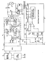
- the drawing illustrates a circuit designed to ignite an HID lamp 5 by providing power to the lamp 5 from a power source through an inverter circuit 4 which has at least one inverter control input and transformer T3, wherein the inverter circuit 4 operates at a frequency higher than a resonant frequency of a resonant tank circuit formed by the transformer T3 and an output capacitor C5.
- This resonant frequency is typically 300 kHz.
- the transformer T3 has a first winding connected to an output of the inverter circuit.
- the circuit warms up the lamp by increasing a current in the lamp 5 until it reaches a predetermined normal operating voltage.
- a control circuit regulates power supplied to the lamp 5 during normal operation to maintain a predetermined power level.
- the control circuit is connected between the power source and the inverter 4 as well as to at least one inverter control input of the inverter 4. With the present invention, lamp starting time is typically 1 minute.
- the HID lamp electronic ballast is powered by an AC line.
- the ballast controls the electrical power supplied to the gas discharge lamp 5, providing the voltage and current required to ignite, warm-up and normally operate the lamp 5.
- EMI Line filter 1 receives the AC line, reduces conducted interference and provides its output to bridge rectifier 2.
- Bridge rectifier 2 provides a rectified sinusoid output to power factor correction (PFC) converter 3.
- PFC converter 3 reduces line harmonic distortion and generates constant DC voltage Vout.
- Vout is applied to full bridge inverter 4 having transformer T3 output. One terminal of Vout passes through current sense element R1.
- Phase shift controller 6 may be, for example, a Unitrode UC1875.
- the UC1875 family of integrated circuits implements control of the bridge power stage by phase shifting the switching of one half bridge with respect to the other, allowing constant frequency pulse-width modulation in combination with resonant, zero-voltage switching for high efficiency performance at high frequencies.
- a secondary winding W2 of transformer T3 is connected to a parallel arrangement of a capacitor C5 and gas discharge lamp 5.
- the output transformer T3 may be constructed using E-cores with a bobbin on which the windings are separately wound.
- the inverter 4 includes transformers T1 and T2, each having first, second, and third windings.
- the first winding of T1 is connected to output terminals Out A and Out B of phase shift controller 6.
- the first winding of T2 is connected to output terminals Out C and Out D of phase shift controller 6.
- the winding nodes to which Out A and Out C are connected are identified with a dot indicating magnetic start of the winding.
- Switches S1 and S3 are arranged in series between the voltage rails of inverter 4, as are switches S2 and S4.
- the windings of transformers T1 and T2 are phased so that when transistors S1 and S4 are on, transistors S2 and S3 are off.
- the switches are shown with their corresponding body diodes D1-D4 and parasitic output capacitances C1-C4.
- Gates of S1 and S2 are connected to magnetic starts (dotted nodes) of the second windings of transformers T1 and T2, respectively.
- Gates of S3 and S4 are connected to undotted nodes of the third windings of transformers T1 and T2, respectively.
- Undotted nodes of the second windings of T1 and T2 are connected between S1/S3 and S2/S4, respectively.
- Dotted nodes of the third windings of both T1 and T2 are connected to the lower voltage rail of inverter 4.
- the nodes of W1 are connected between S1/S3 and S2/S4.
- a sense circuit connecting inverter 4 to phase shift controller 6 includes sampling resistor R1, as well as the series arrangement of R2, R3, R4, and C7, which is connected to the EA Out pin of the phase shift controller 6.
- EA- of the phase shift controller 6 is connected between R3 and R4.
- C6 is arranged parallel to R1/R2.
- a variable resistor R9 is connected between Vref and GND, with the tap connected to EA+.
- the voltage signal from current sense element R1 and the programmed voltage provided at EA+ by the variable resistor R9 are supplied to the control chip internal error amplifier EA for comparison.
- An output of the error amplifier is connected to the EA Out pin as well phase shift and time delay circuitry within the phase shift controller 6.
- the phase shift and time delay circuitry drives provides the signals Out A-Out D of the phase shift controller 6.
- the control loop keeps the inverter input constant during the normal operating phase of the lamp by adjusting Out A-Out D to control inverter 4. Due to constant voltage on the inverter input and constant efficiency, power consumption by the lamp stays approximately constant. Maximum current is achieved when the duty cycle of the signal from the phase shift and time delay circuit is 100%. A reduced duty cycle reduces the current to the load.
- Typical HID lamp voltage during operation is 70-100 volts.
- an ignition circuit is required to temporarily disable the error amplifier (EA) of phase shift controller 6.
- EA error amplifier
- FET switch S5, winding W3 of transformer T3, diode D5, storage capacitor C8 and resistive ignition phase voltage divider R5/R6 perform this function.
- Winding W3 is arranged in close proximity to the secondary winding W2 of transformer T3.
- the nodes of W3 are connected to ground and the anode of D5.
- Storage capacitor C8 is connected to the cathode of D5 and ground.
- Voltage divider R5/R6 is connected from between C8 and D5 to ground.
- the gate of S5 is connected between R5 and R6.
- S5 connects the point between R2 and R3 to ground.
- phase shift controller 6 To provide fault protection, additional circuitry is provided to shut down the phase shift controller 6 in the event of very high voltage.
- overvoltage protection resistive voltage divider R7/R8 is arranged parallel to C8. The point between R7 and R8 is connected to pin CS+ of phase shift controller 6.
- a timing Circuit may be placed between R7/R8 and CS+. The timing circuit may include a flip-flop.
- the HID lamp has three phases of operation: ignition of discharge, warm-up and normal operation. During the various phases, the requirements for electrical energy from the ballast are different.
- the ballast has to provide voltage in the kilovolts range during the ignition phase.
- the lamp voltage is one-half to one-third the voltage at normal operation, and the ballast has to provide increased current to shorten a warm-up time.
- the ballast should provide constant power to the lamp. This is achieved by having the voltage at the output of PFC 3 at a constant DC voltage and maintaining the current to the load at a constant level.
- the present invention provides all these requirements with a minimum number of components while utilizing a simple control structure. It utilizes a Zero Voltage Switching (ZVS) phase shift controlled inverter, operating at high frequency (e.g., 320 kHz), with transformer output and indirect power control. With the inverter frequency higher than the resonant frequency of the tank circuit, the output appears as an inductive load, rather than a capacitive load. In addition to the benefits of simplicity and minimum cost, this solution provides additional benefits like isolated output and small size.
- ZVS Zero Voltage Switching
- Transformer T3 is designed with excessive leakage inductance, providing an inductive component for the resonant tank circuit. During the various phases of the lamp operating cycle, the leakage inductance of the transformer performs different functions in the ballast.
- the present invention uses a resonant ignition.
- leakage inductance of transformer T3 forms the resonant tank with the output capacitor C5 with the resonant frequency slightly less than the operating frequency of the inverter.
- the amplitude of the AC voltage on the lamp increases rapidly until electrical breakdown of the gas in the lamp occurs.
- the output voltage and current rapidly reach substantial values, in the range of 1-10 kV and 0.5-5 A. To allow the inverter to reach these values, the control loop must be blocked during ignition.
- Diode D5 and storage capacitor C8 form a peak voltage detector.
- the DC voltage on the capacitor C8 is proportional to the amplitude of the AC voltage on the winding W2. This voltage is divided by voltage divider network R5/R6 and applied to the gate of FET switch S5.
- FET S5 serves to block the signal from current sense resistor R1, so phase shift controller 6 provides for maximum duty cycle and does not limit resonant voltage and current.
- the transistor S5 remains conducting all the time when voltage on the winding W2 stays high.
- the lamp voltage drops to a value approximately one-half to one-third of the normal operation voltage, increasing gradually until it reaches normal operation voltage.
- This phase is known as the warm-up phase of the operation cycle, and may last from tens of seconds to minutes.
- the phase shift controller 6 increases pulse width in an attempt to provide constant power.
- the control loop cannot regulate input power and the leakage inductance of transformer T3 begins to function as a current limiting element in the circuit.
- the leakage inductance of the transformer is selected such that the lamp current in the absence of control by the phase shift controller 6 is 1.3-1.5 times greater than during normal steady state operation. This reduces the HID lamp warm-up time. During that time, waveforms of voltage and current have close to a triangular shape with slightly rounded tops due to the effect of capacitor C5.
- the lamp voltage reaches the level where power consumption reaches a predetermined level (adjustable with potentiometer R9).
- the control loop then takes over and starts to regulate power supplied to the lamp.
- controller UC1875 maintains constant power to the lamp and ensures high frequency lossless switching of the inverter.
- the voltage signal developed across R1 is compared to a predetermined set voltage as determined by the position of the potentiometer wiper of variable resistor R9 connected to EA+ of the phase shift controller 6.
- the leakage inductance of transformer T3 during the lamp's steady state phase plays the role of an energy storage element, providing energy for recharging the parasitic drain-source capacitances C1-C4 of the inverter FETs S1-S4 and lossless switching.
- the leakage inductance also limits output current to acceptable levels in the case of a short circuit on the output.
- the ballast utilizes parasitic elements of the circuit such as leakage inductance of output transformer and parasitic drain-to-source capacitance of inverter MOSFETs to provide low less operation at high frequency.
- ballast could be implemented with a lamp drive scheme which includes frequency and/or amplitude modulation or control schemes to optimize lamp operation.
Landscapes
- Engineering & Computer Science (AREA)
- Power Engineering (AREA)
- Circuit Arrangements For Discharge Lamps (AREA)
Applications Claiming Priority (2)
| Application Number | Priority Date | Filing Date | Title |
|---|---|---|---|
| US377471 | 1999-08-19 | ||
| US09/377,471 US6181076B1 (en) | 1999-08-19 | 1999-08-19 | Apparatus and method for operating a high intensity gas discharge lamp ballast |
Publications (3)
| Publication Number | Publication Date |
|---|---|
| EP1077591A2 true EP1077591A2 (de) | 2001-02-21 |
| EP1077591A3 EP1077591A3 (de) | 2001-03-07 |
| EP1077591B1 EP1077591B1 (de) | 2003-10-22 |
Family
ID=23489243
Family Applications (1)
| Application Number | Title | Priority Date | Filing Date |
|---|---|---|---|
| EP00116154A Expired - Lifetime EP1077591B1 (de) | 1999-08-19 | 2000-08-01 | Vorschaltgerät für Starkstromgasentladungslampe |
Country Status (7)
| Country | Link |
|---|---|
| US (1) | US6181076B1 (de) |
| EP (1) | EP1077591B1 (de) |
| KR (1) | KR100697463B1 (de) |
| AT (1) | ATE252815T1 (de) |
| CA (1) | CA2313960A1 (de) |
| DE (1) | DE60006046T2 (de) |
| TW (1) | TW508977B (de) |
Cited By (4)
| Publication number | Priority date | Publication date | Assignee | Title |
|---|---|---|---|---|
| KR20010016094A (ko) * | 2000-11-01 | 2001-03-05 | 김기대 | 형광등제어장치 |
| WO2007122114A1 (de) * | 2006-04-20 | 2007-11-01 | Patent-Treuhand-Gesellschaft für elektrische Glühlampen mbH | Anordnung und verfahren zum betreiben einer hochdruck-entladungslampe |
| EP1851601A4 (de) * | 2004-08-12 | 2010-04-07 | Charles J Montante | Ballaststromversorgung |
| US7982405B2 (en) | 2005-03-22 | 2011-07-19 | Lightech Electronic Industries Ltd. | Igniter circuit for an HID lamp |
Families Citing this family (25)
| Publication number | Priority date | Publication date | Assignee | Title |
|---|---|---|---|---|
| US6479949B1 (en) * | 2000-02-01 | 2002-11-12 | General Electric Company | Power regulation circuit for high frequency electronic ballast for ceramic metal halide lamp |
| JP2004504708A (ja) * | 2000-07-21 | 2004-02-12 | オスラム−シルヴェニア インコーポレイテッド | アーク検出及び電子安定器の保護のための方法及び装置 |
| US6476566B2 (en) * | 2000-12-27 | 2002-11-05 | Infocus Systems, Inc. | Method and apparatus for canceling ripple current in a lamp |
| EP1227706B1 (de) * | 2001-01-24 | 2012-11-28 | City University of Hong Kong | Neue Schaltungsentwürfe und Steuerungstechniken für elektronische Hochfrequenz-Vorschaltgeräte für Entladungslampen hoher Intensität |
| US6515431B2 (en) * | 2001-02-05 | 2003-02-04 | Yin Nan Enterprises Co., Ltd. | Multi-lamp protection circuit for an electronic ballast |
| US6577078B2 (en) * | 2001-09-26 | 2003-06-10 | Koninklijke Philips Electronics N.V. | Electronic ballast with lamp run-up current regulation |
| US6680585B2 (en) | 2001-12-17 | 2004-01-20 | Osram Sylvania Inc. | Method and apparatus for modulating HID ballast operating frequency using DC bus ripple voltage |
| DE10200022A1 (de) * | 2002-01-02 | 2003-07-17 | Philips Intellectual Property | Schaltungsanordnung zum Betrieb einer oder mehrerer Lampen |
| DE10319950A1 (de) * | 2003-05-02 | 2004-11-18 | Patent-Treuhand-Gesellschaft für elektrische Glühlampen mbH | Betriebsgerät und Verfahren zum Betreiben von Gasentladungslampen |
| FR2864066B1 (fr) * | 2003-12-23 | 2006-04-14 | Otv Sa | Dispositif d'alimentation de lampes uv utilisees dans le cadre du traitement de l'eau |
| CN2692959Y (zh) * | 2004-02-11 | 2005-04-13 | 姚流文 | 高强度气体放电灯电子控制器 |
| US7112929B2 (en) * | 2004-04-01 | 2006-09-26 | Microsemi Corporation | Full-bridge and half-bridge compatible driver timing schedule for direct drive backlight system |
| US7397199B2 (en) * | 2004-10-27 | 2008-07-08 | Harison Toshiba Lighting Corp. | Discharge lamp lighting device |
| TWI323866B (en) * | 2006-01-06 | 2010-04-21 | Himax Tech Ltd | An inverter-driving device and method |
| JP2007335267A (ja) * | 2006-06-15 | 2007-12-27 | Minebea Co Ltd | 放電灯点灯装置 |
| US7276859B1 (en) * | 2006-09-28 | 2007-10-02 | Osram Sylvania Inc. | Three-phase electronic ballast with improved three-phase EMI filter |
| PL2102978T3 (pl) | 2006-12-20 | 2016-12-30 | Aparat zasilający do obciążenia pojemnościowego | |
| KR100856386B1 (ko) * | 2007-01-11 | 2008-09-04 | 대성전기공업 주식회사 | 에이치아이디 램프 안정기 |
| US8199545B2 (en) * | 2009-05-05 | 2012-06-12 | Hamilton Sundstrand Corporation | Power-conversion control system including sliding mode controller and cycloconverter |
| DE102009030106B4 (de) | 2009-06-22 | 2015-07-30 | Minebea Co., Ltd. | Verfahren zur Ansteuerung von Gasentladungslampen |
| CA2767628A1 (en) * | 2009-07-09 | 2011-01-13 | Enphase Energy, Inc. | Method and apparatus for single-path control and monitoring of an h-bridge |
| CN102194648A (zh) * | 2010-02-24 | 2011-09-21 | 皇家飞利浦电子股份有限公司 | Hid照明系统 |
| CN102238793B (zh) | 2011-07-18 | 2014-04-16 | 台达电子企业管理(上海)有限公司 | 高强度气体放电灯控制电路及控制方法 |
| RU2479166C1 (ru) * | 2011-10-05 | 2013-04-10 | Федеральное государственное бюджетное образовательное учреждение высшего профессионального образования "Ставропольский государственный аграрный университет" | Пускорегулирующее устройство для газоразрядных ламп высокого давления |
| TWI481313B (zh) * | 2013-03-11 | 2015-04-11 | Inergy Technology Inc | 可偵測零電壓切換之安定器之驅動器 |
Family Cites Families (15)
| Publication number | Priority date | Publication date | Assignee | Title |
|---|---|---|---|---|
| US4415839A (en) | 1981-11-23 | 1983-11-15 | Lesea Ronald A | Electronic ballast for gaseous discharge lamps |
| BR8305740A (pt) * | 1982-01-15 | 1984-01-10 | Minitronics Pty Ltd | Lastro eletronico de alta frequencia para lampadas de descarga eletro-gasosa |
| US4560908A (en) * | 1982-05-27 | 1985-12-24 | North American Philips Corporation | High-frequency oscillator-inverter ballast circuit for discharge lamps |
| US4717863A (en) * | 1986-02-18 | 1988-01-05 | Zeiler Kenneth T | Frequency modulation ballast circuit |
| US4904904A (en) * | 1987-11-09 | 1990-02-27 | Lumintech, Inc. | Electronic transformer system for powering gaseous discharge lamps |
| FR2700535B1 (fr) * | 1993-01-19 | 1995-04-14 | Hoechst France | Procédé continu de fabrication industrielle du diméthoxyéthanal. |
| US5796216A (en) * | 1993-07-16 | 1998-08-18 | Delta Power Supply, Inc. | Electronic ignition enhancing circuit having both fundamental and harmonic resonant circuits as well as a DC offset |
| US5623187A (en) | 1994-12-28 | 1997-04-22 | Philips Electronics North America Corporation | Controller for a gas discharge lamp with variable inverter frequency and with lamp power and bus voltage control |
| US5850127A (en) | 1996-05-10 | 1998-12-15 | Philips Electronics North America Corporation | EBL having a feedback circuit and a method for ensuring low temperature lamp operation at low dimming levels |
| US5719474A (en) | 1996-06-14 | 1998-02-17 | Loral Corporation | Fluorescent lamps with current-mode driver control |
| US5877592A (en) * | 1996-11-01 | 1999-03-02 | Magnetek, Inc. | Programmed-start parallel-resonant electronic ballast |
| US5889373A (en) * | 1996-12-30 | 1999-03-30 | General Electric Company | Fluorescent lamp ballast with current feedback using a dual-function magnetic device |
| US6088249A (en) * | 1997-12-02 | 2000-07-11 | Power Circuit Innovations, Inc. | Frequency modulated ballast with loosely coupled transformer |
| US5933340A (en) * | 1997-12-02 | 1999-08-03 | Power Circuit Innovations, Inc. | Frequency controller with loosely coupled transformer having a shunt with a gap and method therefor |
| US6094017A (en) * | 1997-12-02 | 2000-07-25 | Power Circuit Innovations, Inc. | Dimming ballast and drive method for a metal halide lamp using a frequency controlled loosely coupled transformer |
-
1999
- 1999-08-19 US US09/377,471 patent/US6181076B1/en not_active Expired - Lifetime
-
2000
- 2000-07-06 CA CA002313960A patent/CA2313960A1/en not_active Abandoned
- 2000-08-01 DE DE60006046T patent/DE60006046T2/de not_active Expired - Lifetime
- 2000-08-01 AT AT00116154T patent/ATE252815T1/de not_active IP Right Cessation
- 2000-08-01 EP EP00116154A patent/EP1077591B1/de not_active Expired - Lifetime
- 2000-08-03 TW TW089115579A patent/TW508977B/zh not_active IP Right Cessation
- 2000-08-18 KR KR1020000047763A patent/KR100697463B1/ko not_active Expired - Fee Related
Cited By (4)
| Publication number | Priority date | Publication date | Assignee | Title |
|---|---|---|---|---|
| KR20010016094A (ko) * | 2000-11-01 | 2001-03-05 | 김기대 | 형광등제어장치 |
| EP1851601A4 (de) * | 2004-08-12 | 2010-04-07 | Charles J Montante | Ballaststromversorgung |
| US7982405B2 (en) | 2005-03-22 | 2011-07-19 | Lightech Electronic Industries Ltd. | Igniter circuit for an HID lamp |
| WO2007122114A1 (de) * | 2006-04-20 | 2007-11-01 | Patent-Treuhand-Gesellschaft für elektrische Glühlampen mbH | Anordnung und verfahren zum betreiben einer hochdruck-entladungslampe |
Also Published As
| Publication number | Publication date |
|---|---|
| KR20010050116A (ko) | 2001-06-15 |
| US6181076B1 (en) | 2001-01-30 |
| CA2313960A1 (en) | 2001-02-19 |
| DE60006046T2 (de) | 2004-05-19 |
| DE60006046D1 (de) | 2003-11-27 |
| EP1077591B1 (de) | 2003-10-22 |
| EP1077591A3 (de) | 2001-03-07 |
| ATE252815T1 (de) | 2003-11-15 |
| KR100697463B1 (ko) | 2007-03-20 |
| TW508977B (en) | 2002-11-01 |
Similar Documents
| Publication | Publication Date | Title |
|---|---|---|
| EP1077591B1 (de) | Vorschaltgerät für Starkstromgasentladungslampe | |
| US7061188B1 (en) | Instant start electronic ballast with universal AC input voltage | |
| CA2224300C (en) | Discharge lamp driving bridge circuit | |
| US6819057B2 (en) | Ballast self oscillating inverter with phase controlled voltage feedback | |
| AU2010202097A1 (en) | Electronic high intensity discharge lamp driver | |
| RU2390977C2 (ru) | Устройство и способ для эксплуатации газоразрядных ламп | |
| JPH03102798A (ja) | ガス放電ランプの始動及び点灯用回路装置 | |
| KR101548520B1 (ko) | 프로그램 개시 안정기 | |
| JP3760074B2 (ja) | 放電灯点灯回路 | |
| JP2001006890A (ja) | 放電灯点灯回路 | |
| US7164239B2 (en) | Discharge lamp ballast circuit | |
| US7145293B2 (en) | Electronic ballast having resonance excitation for generating a transfer voltage | |
| US6144173A (en) | Single switch electronic ballast | |
| JPH06124790A (ja) | 高圧放電灯点灯装置及び放電灯点灯装置 | |
| JP3769993B2 (ja) | 放電灯点灯装置 | |
| US20070164685A1 (en) | Discharge lamp lighting apparatus | |
| JP3713129B2 (ja) | 放電灯点灯装置 | |
| JP3593901B2 (ja) | 点灯装置 | |
| JPH0896982A (ja) | 照明装置 | |
| JP2859365B2 (ja) | 交流放電ランプ点灯装置 | |
| KR200231599Y1 (ko) | 고압방전 램프용 전자식 안정기의 구동용 변압기 | |
| JPH03283394A (ja) | 交流放電ランプ点灯装置 | |
| JPH04292896A (ja) | 放電灯点灯回路 | |
| JP2007165127A (ja) | 放電灯点灯装置 | |
| JP2004193075A (ja) | 放電灯点灯装置 |
Legal Events
| Date | Code | Title | Description |
|---|---|---|---|
| PUAI | Public reference made under article 153(3) epc to a published international application that has entered the european phase |
Free format text: ORIGINAL CODE: 0009012 |
|
| PUAL | Search report despatched |
Free format text: ORIGINAL CODE: 0009013 |
|
| AK | Designated contracting states |
Kind code of ref document: A2 Designated state(s): AT BE CH CY DE DK ES FI FR GB GR IE IT LI LU MC NL PT SE |
|
| AX | Request for extension of the european patent |
Free format text: AL;LT;LV;MK;RO;SI |
|
| AK | Designated contracting states |
Kind code of ref document: A3 Designated state(s): AT BE CH CY DE DK ES FI FR GB GR IE IT LI LU MC NL PT SE |
|
| AX | Request for extension of the european patent |
Free format text: AL;LT;LV;MK;RO;SI |
|
| 17P | Request for examination filed |
Effective date: 20010402 |
|
| 17Q | First examination report despatched |
Effective date: 20010523 |
|
| AKX | Designation fees paid |
Free format text: AT BE CH CY DE DK ES FI FR GB GR IE IT LI LU MC NL PT SE |
|
| GRAH | Despatch of communication of intention to grant a patent |
Free format text: ORIGINAL CODE: EPIDOS IGRA |
|
| GRAS | Grant fee paid |
Free format text: ORIGINAL CODE: EPIDOSNIGR3 |
|
| GRAA | (expected) grant |
Free format text: ORIGINAL CODE: 0009210 |
|
| AK | Designated contracting states |
Kind code of ref document: B1 Designated state(s): AT BE CH CY DE DK ES FI FR GB GR IE IT LI LU MC NL PT SE |
|
| PG25 | Lapsed in a contracting state [announced via postgrant information from national office to epo] |
Ref country code: AT Free format text: LAPSE BECAUSE OF FAILURE TO SUBMIT A TRANSLATION OF THE DESCRIPTION OR TO PAY THE FEE WITHIN THE PRESCRIBED TIME-LIMIT Effective date: 20031022 Ref country code: CY Free format text: LAPSE BECAUSE OF FAILURE TO SUBMIT A TRANSLATION OF THE DESCRIPTION OR TO PAY THE FEE WITHIN THE PRESCRIBED TIME-LIMIT Effective date: 20031022 Ref country code: ES Free format text: LAPSE BECAUSE OF FAILURE TO SUBMIT A TRANSLATION OF THE DESCRIPTION OR TO PAY THE FEE WITHIN THE PRESCRIBED TIME-LIMIT Effective date: 20031022 Ref country code: FI Free format text: LAPSE BECAUSE OF FAILURE TO SUBMIT A TRANSLATION OF THE DESCRIPTION OR TO PAY THE FEE WITHIN THE PRESCRIBED TIME-LIMIT Effective date: 20031022 |
|
| REG | Reference to a national code |
Ref country code: GB Ref legal event code: FG4D |
|
| REG | Reference to a national code |
Ref country code: CH Ref legal event code: NV Representative=s name: SIEMENS SCHWEIZ AG Ref country code: CH Ref legal event code: EP |
|
| REG | Reference to a national code |
Ref country code: IE Ref legal event code: FG4D |
|
| REF | Corresponds to: |
Ref document number: 60006046 Country of ref document: DE Date of ref document: 20031127 Kind code of ref document: P |
|
| PG25 | Lapsed in a contracting state [announced via postgrant information from national office to epo] |
Ref country code: GR Free format text: LAPSE BECAUSE OF FAILURE TO SUBMIT A TRANSLATION OF THE DESCRIPTION OR TO PAY THE FEE WITHIN THE PRESCRIBED TIME-LIMIT Effective date: 20040122 Ref country code: DK Free format text: LAPSE BECAUSE OF FAILURE TO SUBMIT A TRANSLATION OF THE DESCRIPTION OR TO PAY THE FEE WITHIN THE PRESCRIBED TIME-LIMIT Effective date: 20040122 Ref country code: SE Free format text: LAPSE BECAUSE OF FAILURE TO SUBMIT A TRANSLATION OF THE DESCRIPTION OR TO PAY THE FEE WITHIN THE PRESCRIBED TIME-LIMIT Effective date: 20040122 |
|
| ET | Fr: translation filed | ||
| PG25 | Lapsed in a contracting state [announced via postgrant information from national office to epo] |
Ref country code: LU Free format text: LAPSE BECAUSE OF NON-PAYMENT OF DUE FEES Effective date: 20040801 |
|
| PG25 | Lapsed in a contracting state [announced via postgrant information from national office to epo] |
Ref country code: IE Free format text: LAPSE BECAUSE OF NON-PAYMENT OF DUE FEES Effective date: 20040802 |
|
| PLBE | No opposition filed within time limit |
Free format text: ORIGINAL CODE: 0009261 |
|
| STAA | Information on the status of an ep patent application or granted ep patent |
Free format text: STATUS: NO OPPOSITION FILED WITHIN TIME LIMIT |
|
| PG25 | Lapsed in a contracting state [announced via postgrant information from national office to epo] |
Ref country code: MC Free format text: LAPSE BECAUSE OF NON-PAYMENT OF DUE FEES Effective date: 20040831 |
|
| 26N | No opposition filed |
Effective date: 20040723 |
|
| REG | Reference to a national code |
Ref country code: IE Ref legal event code: MM4A |
|
| PGFP | Annual fee paid to national office [announced via postgrant information from national office to epo] |
Ref country code: NL Payment date: 20060803 Year of fee payment: 7 |
|
| PG25 | Lapsed in a contracting state [announced via postgrant information from national office to epo] |
Ref country code: PT Free format text: LAPSE BECAUSE OF NON-PAYMENT OF DUE FEES Effective date: 20040322 |
|
| PG25 | Lapsed in a contracting state [announced via postgrant information from national office to epo] |
Ref country code: NL Free format text: LAPSE BECAUSE OF NON-PAYMENT OF DUE FEES Effective date: 20080301 |
|
| NLV4 | Nl: lapsed or anulled due to non-payment of the annual fee |
Effective date: 20080301 |
|
| REG | Reference to a national code |
Ref country code: CH Ref legal event code: PCAR Free format text: SIEMENS SCHWEIZ AG;INTELLECTUAL PROPERTY FREILAGERSTRASSE 40;8047 ZUERICH (CH) |
|
| PGFP | Annual fee paid to national office [announced via postgrant information from national office to epo] |
Ref country code: FR Payment date: 20100901 Year of fee payment: 11 Ref country code: IT Payment date: 20100825 Year of fee payment: 11 |
|
| PGFP | Annual fee paid to national office [announced via postgrant information from national office to epo] |
Ref country code: GB Payment date: 20100812 Year of fee payment: 11 |
|
| PGFP | Annual fee paid to national office [announced via postgrant information from national office to epo] |
Ref country code: BE Payment date: 20100817 Year of fee payment: 11 |
|
| PGFP | Annual fee paid to national office [announced via postgrant information from national office to epo] |
Ref country code: CH Payment date: 20111117 Year of fee payment: 12 |
|
| BERE | Be: lapsed |
Owner name: *OSRAM SYLVANIA INC. Effective date: 20110831 |
|
| GBPC | Gb: european patent ceased through non-payment of renewal fee |
Effective date: 20110801 |
|
| REG | Reference to a national code |
Ref country code: FR Ref legal event code: ST Effective date: 20120430 |
|
| PG25 | Lapsed in a contracting state [announced via postgrant information from national office to epo] |
Ref country code: IT Free format text: LAPSE BECAUSE OF NON-PAYMENT OF DUE FEES Effective date: 20110801 Ref country code: BE Free format text: LAPSE BECAUSE OF NON-PAYMENT OF DUE FEES Effective date: 20110831 |
|
| PG25 | Lapsed in a contracting state [announced via postgrant information from national office to epo] |
Ref country code: GB Free format text: LAPSE BECAUSE OF NON-PAYMENT OF DUE FEES Effective date: 20110801 Ref country code: FR Free format text: LAPSE BECAUSE OF NON-PAYMENT OF DUE FEES Effective date: 20110831 |
|
| REG | Reference to a national code |
Ref country code: CH Ref legal event code: PL |
|
| PG25 | Lapsed in a contracting state [announced via postgrant information from national office to epo] |
Ref country code: LI Free format text: LAPSE BECAUSE OF NON-PAYMENT OF DUE FEES Effective date: 20120831 Ref country code: CH Free format text: LAPSE BECAUSE OF NON-PAYMENT OF DUE FEES Effective date: 20120831 |
|
| PGFP | Annual fee paid to national office [announced via postgrant information from national office to epo] |
Ref country code: DE Payment date: 20130821 Year of fee payment: 14 |
|
| REG | Reference to a national code |
Ref country code: DE Ref legal event code: R119 Ref document number: 60006046 Country of ref document: DE |
|
| REG | Reference to a national code |
Ref country code: DE Ref legal event code: R119 Ref document number: 60006046 Country of ref document: DE Effective date: 20150303 |
|
| PG25 | Lapsed in a contracting state [announced via postgrant information from national office to epo] |
Ref country code: DE Free format text: LAPSE BECAUSE OF NON-PAYMENT OF DUE FEES Effective date: 20150303 |