EP1074049B1 - Method and apparatus for distributing an optical clock in an integrated circuit - Google Patents
Method and apparatus for distributing an optical clock in an integrated circuit Download PDFInfo
- Publication number
- EP1074049B1 EP1074049B1 EP98918181A EP98918181A EP1074049B1 EP 1074049 B1 EP1074049 B1 EP 1074049B1 EP 98918181 A EP98918181 A EP 98918181A EP 98918181 A EP98918181 A EP 98918181A EP 1074049 B1 EP1074049 B1 EP 1074049B1
- Authority
- EP
- European Patent Office
- Prior art keywords
- clock
- semiconductor
- integrated circuit
- laser
- clocking
- Prior art date
- Legal status (The legal status is an assumption and is not a legal conclusion. Google has not performed a legal analysis and makes no representation as to the accuracy of the status listed.)
- Expired - Lifetime
Links
Images


Classifications
-
- H—ELECTRICITY
- H01—ELECTRIC ELEMENTS
- H01S—DEVICES USING THE PROCESS OF LIGHT AMPLIFICATION BY STIMULATED EMISSION OF RADIATION [LASER] TO AMPLIFY OR GENERATE LIGHT; DEVICES USING STIMULATED EMISSION OF ELECTROMAGNETIC RADIATION IN WAVE RANGES OTHER THAN OPTICAL
- H01S5/00—Semiconductor lasers
- H01S5/06—Arrangements for controlling the laser output parameters, e.g. by operating on the active medium
- H01S5/068—Stabilisation of laser output parameters
- H01S5/06812—Stabilisation of laser output parameters by monitoring or fixing the threshold current or other specific points of the L-I or V-I characteristics
-
- G—PHYSICS
- G06—COMPUTING OR CALCULATING; COUNTING
- G06F—ELECTRIC DIGITAL DATA PROCESSING
- G06F1/00—Details not covered by groups G06F3/00 - G06F13/00 and G06F21/00
- G06F1/04—Generating or distributing clock signals or signals derived directly therefrom
- G06F1/10—Distribution of clock signals, e.g. skew
- G06F1/105—Distribution of clock signals, e.g. skew in which the distribution is at least partially optical
-
- H—ELECTRICITY
- H01—ELECTRIC ELEMENTS
- H01S—DEVICES USING THE PROCESS OF LIGHT AMPLIFICATION BY STIMULATED EMISSION OF RADIATION [LASER] TO AMPLIFY OR GENERATE LIGHT; DEVICES USING STIMULATED EMISSION OF ELECTROMAGNETIC RADIATION IN WAVE RANGES OTHER THAN OPTICAL
- H01S5/00—Semiconductor lasers
- H01S5/04—Processes or apparatus for excitation, e.g. pumping, e.g. by electron beams
- H01S5/042—Electrical excitation ; Circuits therefor
- H01S5/0428—Electrical excitation ; Circuits therefor for applying pulses to the laser
-
- H—ELECTRICITY
- H01—ELECTRIC ELEMENTS
- H01S—DEVICES USING THE PROCESS OF LIGHT AMPLIFICATION BY STIMULATED EMISSION OF RADIATION [LASER] TO AMPLIFY OR GENERATE LIGHT; DEVICES USING STIMULATED EMISSION OF ELECTROMAGNETIC RADIATION IN WAVE RANGES OTHER THAN OPTICAL
- H01S5/00—Semiconductor lasers
- H01S5/10—Construction or shape of the optical resonator, e.g. extended or external cavity, coupled cavities, bent-guide, varying width, thickness or composition of the active region
- H01S5/18—Surface-emitting [SE] lasers, e.g. having both horizontal and vertical cavities
- H01S5/183—Surface-emitting [SE] lasers, e.g. having both horizontal and vertical cavities having only vertical cavities, e.g. vertical cavity surface-emitting lasers [VCSEL]
- H01S5/18383—Surface-emitting [SE] lasers, e.g. having both horizontal and vertical cavities having only vertical cavities, e.g. vertical cavity surface-emitting lasers [VCSEL] with periodic active regions at nodes or maxima of light intensity
Definitions
- the present invention relates generally to integrated circuit clocking and, more specifically, the present invention relates to optical clock distribution networks in integrated circuits.
- Clock skew is the difference in arrival times of clock edges to different parts of the chip. Synchronous digital logic requires precise clocks for the latching data. Ideal synchronous logic relies on clocks arriving simultaneously to all the circuits. Clock skew reduces the maximum operating frequency of the circuit as the circuit has to be designed for worst case skew for it to operate reliably.
- the principle cause of clock skew in the global clock distribution of an integrated circuit is the variation in the routing impedance of the clock distribution within the die. Hence clock skew arises even with an equal length clock distribution network such as an H-Tree.
- clock skew budget is approximately 10% of the cycle time.
- the tolerable clock skew is less than or equal to 100 ps.
- VLSI clock frequencies increase beyond 1 GHz, the requirement on the clock skew becomes more challenging.
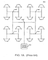
- FIG. 1 A is a diagram illustrating such a hierarchical H-tree clock distribution network 101 that is implemented in high speed integrated circuits to reduce or eliminate the clock skew effect.
- a clock driver 103 is used to drive H-tree network 101 at the center node 105. It is appreciated that clock driver 103 is typically a very large driver in order to provide sufficient drive to H-tree network 101, which typically has a large capacitance in today's complex high speed integrated circuits.
- the clock paths of the "H" formed between nodes 107, 109, 111 and 113 have equal lengths between center node 105 and each of the peripheral points of the "H" at nodes 107, 109, 111 and 113. Therefore, assuming a uniform propagation delay of a clock signal per unit length of the H-tree network 101, there should be no clock skew between the clock signal supplied to nodes 107, 109, 111 and 113 from clock driver 103.
- FIG. 1A further illustrates H-tree network 101 taken to another hierarchical level with an "H" coupled to each respective peripheral node of the first level "H.” Accordingly, every peripheral node 115 is an equal distance from node 107. Every peripheral node 117 is an equal distance from node 109. Every peripheral node 119 is an equal distance from node 111. Finally, every peripheral node 121 is an equal distance from node 113. Therefore, the clock paths from all nodes labeled 115, 117, 119 and 121 are an equal distance from clock driver 103 and therefore should have no clock skew between them since the clock delay from clock driver 103 should be equal to all peripheral nodes of the H-tree network 101.
- each node 115, 117, 119 and 121 can be configured to act as a receiving station for a clock signal and service the clocking requirements of an area of the integrated circuit near the node with negligible clock skew with reference to the other similarly configured nodes of the H-tree network 101.
- clock skew continues to be a challenging issue, even with an H-tree network 101 since the H-tree network 101 clock lines do not always have uniform characteristic impedance. As a result, there may be a non-uniform propagation delay of a clock signal traveling through the paths of the H-tree network 101 even though nodes 115, 117, 119 and 121 are in equal distance from clock driver 103. Consequently, there is an unpredictable clock skew at the end points of the H-tree clock distribution network 101.
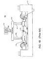
- FIG. 1B An off chip optical source 153 generates an optical clock signal 155 which is split with hologram 157 into split beams 159 and 161.
- a direct line of sight is provided to the detectors 163 and 165 from the front side surface 179 of integrated circuit die 171 to receive split beams 159 and 161 respectively.
- Clock signal 167 is generated by detector 163 and clock signal 169 is generated by detector 165. Since the clock signal is then locally distributed from the detectors 163 and 165 using on chip metal interconnects clock signals 167 and 169 are available to clock their respective areas of the integrated circuit.
- C4 packaged chips sometimes referred to as flip chip
- C4/MCM multi chip modules
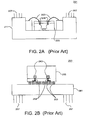
- Figure 2B is an illustration of a C4 packaged chip 251.
- C4 is the packaging of choice for future high frequency chips as it provides high density low inductance connections using ball bonds 253 between chip 255 and package 261 by eliminating the high inductance bond wires as are used in today's wire bond packages.
- Figure 2A is an illustration of a chip 201 using today's wire bond packages. As shown in Figure 2A, wire bonds 203 are used for connections between package 211 and chip 205.
- the front side of the chip is no longer accessible and with the prior art optical routing, the routing would need to be integrated into the package itself. This places extremely complex constraints on the design of the C4 substrate which now has to have both electrical and optical routing.
- Another important problem with the prior art optical distribution network 151 is that the requirement of locating detectors 163 and 165 in the line of sight of split beams 159 and 161 from the front side surface 179 of integrated circuit 171 is a challenging task with modern integrated circuits which typically utilize five or more metal interconnect layers. With the stacking of a large number of metal interconnect layers, creating a line of sight between the split beams 159 and 161 and detectors 163 and 165, without incurring routing congestion becomes an extremely challenging task. This is because line of sight implies that there should be no metal routing at any level of interconnect above the P-N junction detectors. Hence the P-N junction detectors become routing obstacles and as the number of detectors increases this leads to an increase in the die size which generally reduces manufacturing yields and performance.
- EP-A-588746 discloses a method of clocking integrated circuit chips using a pulsed laser to strike an IC module substrate.
- the IC module substrate diffuses the laser beam which then exits the opposite surface of the substrate as diffused light pulses.
- An IC chip mounted on the top surface of the substrate has at least one optical receiver which receives the pulsed energy from the diffused light pulses and converts the light pulses to electrical pulses that clock the chip.
- clock distribution network that overcomes the problems of the prior art.
- Such a clock distribution network would provide minimal clock skew to high speed, high power integrated circuits packaged into C4 (flip chip) and C4/MCM packaging and be fully compatible with the back side heat sink attachment for these packages.
- the clock distribution network should reduce the power dissipation due to global clock distribution by eliminating the large capacitive load of the global network.
- such a clock distribution network should not interfere with on chip signal routing and would be able to provide low skew clock distribution as integrated circuit chips increase in size, complexity and operate at increasing clock frequencies.
- the present invention relates to an improved receiver station for an optical clock distribution network for an integrated circuit.
- a receiver station for an optical clock distribution network as claimed in claim 1 herein.
- the present invention provides a method and apparatus for clocking an integrated circuit by bringing in optical clock signals through the back side of the semiconductor with a mode locked or modulated infrared or visible laser and focusing the light into P-N junction receivers embedded in the integrated chip circuitry through the silicon substrate.
- the present invention includes the advantage of employing optical techniques that can be used without disturbing the conventional CMOS process and C4 packaging technology.
- the beam splitting and focusing elements in one example may be fabricated into optical elements separate from the silicon or optical wave guides may be deposited or micro-machined on the silicon backside.
- an off chip infrared laser is configured as an optical clock to generate and emit infrared laser pulses at a desired clock frequency. Since silicon is partially transparent to infrared light, the laser pulses may be configured to penetrate the silicon and may be focused into receiving stations that include P-N junctions disposed within the silicon to create photocurrents. It is appreciated that heavily doped silicon is partially transparent to infrared radiation at a wavelength that is just around the silicon band gap. In particular, the band gap of intrinsic silicon at room temperature is 1.11 eV. Heavy doping causes the band gap to shrink by around 100 meV to 1.01 eV.
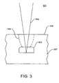
- FIG. 3 shows a portion of a receiving station 301 in accordance with the teachings of the present invention, which includes a P-N junction 303 disposed in a semiconductor 307.
- semiconductor 307 is made of silicon. It is appreciated that semiconductor 307 is part of a C4 packaged integrated circuit such that the back side 305 of the integrated circuit is therefore exposed.
- an infrared laser pulse 309 may be focused through the back side 305 of semiconductor 307 into P-N junction 303.
- the laser pulse 309 is optically split and focused through the back side 305 of semiconductor 307 into to a number of similarly configured P-N junctions 303.
- a Neodymium: Yttrium, Lithium Fluoride (Nd:YLF) laser is utilized, which generates photons with a wavelength of 1.054 ⁇ m, and an energy of approximately 1.178 eV.
- the Nd:YLF photons from the infrared laser can be transmitted through the silicon from the back side directly into photo receiver diodes, or P-N junctions, embedded in the circuitry of a C4 packaged chip.
- the laser radiation will penetrate the silicon and generate photocurrents in P-N junctions.
- the transmission of the photons of a laser having a wavelength of 1.06 ⁇ m has been measured to be approximately 1-2% through a substrate approximately 720 ⁇ m thick.
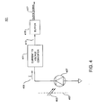
- FIG 4 is an illustration of a receiving station 401 in accordance with the teachings of the present invention, which includes a photo detector 407 disposed in a semiconductor with a laser pulse 403 focused on the photo detector 407 through the back side 405 of the semiconductor.
- a photocurrent I409 is generated which is converted to a voltage V 413 with a current to voltage converter 411.
- Voltage V 413 is buffered with buffer 415 to generate clock signal 417.
- photo detector 407 is a P-N junction disposed in the semiconductor.
- a plurality of receiving stations 401 may be distributed throughout the integrated circuit die to provide clock signal 417 to clock a designated area of the integrated circuit.
- clock signal 417 clocks an area of the integrated circuit near receiving station 401. By having a plurality of receiver stations 401 to generate clock signals 417, the clock can be optically distributed throughout the integrated circuit with minimal clock skew.
- Photo detector 407, current to voltage converter 411 and buffer 415 are optimized for sensitivity and jitter since it is appreciated that the actual chip skew is determined in part by the degree of matching of receiving stations 401 across the die.
- the amount of local buffering employed in each receiving station 401 impacts actual clock skew since each additional local buffering stage correspondingly introduces additional clock skew.
- FIG. 5 is an illustration of the presently described optical clock distribution network 501.
- a master laser 503 is configured to emit master laser pulses 505 at a desired clock frequency.
- An optics element 507 receives master laser pulses 505 and generates split laser pulses 509A-J as shown in Figure 5.
- optical element 507 uses well known techniques to split, collimate and focus split laser beams 509A-J into P-N junctions 515A-J through the back side 511 of a semiconductor 513 of a C4 packaged integrated circuit.
- Each P-N junction 515A-J is separately included in a receiving station similar to that described in Figures 3 and 4 above. Accordingly, a separate clock signal may be generated by each P-N junction 515A-J and may therefore be used to clock a specific area of circuitry in the integrated circuit.
- the clock of the integrated circuit is optically distributed throughout the chip thereby removing the clock distribution network from the silicon and thus eliminating the problems associated with prior art clock distribution networks such as the H-tree network 101 discussed in Figure above.
- optical clock distribution network 501 does not interfere with chip signal routing. Since access to P-N junctions 515A-J is not obstructed by metal interconnects or a package substrate, in contrast with the prior art, providing line of sight to P-N junctions 515A-J in the present invention do not result in the same complex routing requirements and congestion of metal interconnects 173 of prior art optical clock distribution network 151.
- the path lengths of master laser beam 505 through split laser beams 509A-J into P-N junctions 515A-J are all made equal length to minimize any clock skew between each P-N junction 515A-J.
- controlled skew is easily achieved with the present invention by deliberately delaying the optical signal by implementing a longer optical path length within optical element 507.
- optical element 507 is connected to laser 503 with an optical fiber.
- optical element 507 is disposed between the silicon of substrate 513 and a heat sink (not shown). In that embodiment, optical element 507 is sandwiched between the silicon and the heat sink using well known techniques such that heat is sufficiently dissipated from the integrated circuit die.
- optics element 507 splits, collimates and focuses laser beams 509A-J into P-N junctions 515A-J using well known techniques.
- optics element 507 includes a fiber optic system which is employed to split the laser power and distribute and focus it into P-N junctions 515A-J.
- This embodiment includes individual microlenses at the ends of the fiber optic elements and any required matching of the silicon/air refractive index to maximize the light coupling into the silicon.
- optics element 507 includes etch phase hologram gratings directly on the silicon back side for splitting and focusing the infrared laser light. This embodiment has the advantage of self aligning the fan-out beams of the receivers to the accuracy of the lithographic registration of the manufacturing process used.
- optics element 507 includes wave guides fabricated from glass or a polymeric on the silicon back side to split, bend, collimate and focus laser beams 509A-J into P-N junctions 515A-J.
- FIG. 6 is an illustration of another example of the presently described optical clock distribution network 601, which includes a master laser 603 emitting laser pulses 605 at a clock frequency into an optics element 607.
- Optics element 607 splits master laser beam 605 into split laser beams 609A-D and 609G-J.
- Split laser beams 609A-D are focused into P-N junctions 615A-D through the back side 611 of semiconductor 613.
- Split laser beams 609G-J are focused into P-N junctions 615G-J through back side 612 of another semiconductor 614.
- semiconductors 613 and 614 are not included in the same chip. Accordingly, the present optical clock distribution network provides a clock signal to all of the receiving stations with extremely low clock skew to multiple chips in a computer system.
- semiconductors 613 and 614 are the integrated circuit dies of a multi-chip module. In another example, semiconductors 613 and 614 are included in the integrated circuit dies of an entire computer system. That is, optical clock distribution network 601 provides the clock for an entire computer system with minimal dock skew and is therefore not limited to merely providing a clock signal for a single integrated circuit die.
- Each integrated circuit die of the present invention includes P-N junctions 615 to generate a local clock signal to clock a nearby area on the integrated circuit.
- FIG. 7 is an illustration of another example of an optical clock distribution network 701 in the present invention.
- Master laser 703 is configured to emit master laser pulses 705 at a desired clock frequency into optics element 707, which splits master laser beam 705 into split laser beams 709A-J.
- optics element 707 which splits master laser beam 705 into split laser beams 709A-J.
- recesses 717A-J have been added to semiconductor 713 on the back side 711 to locally thin the semiconductor 713 disposed between P-N junctions 715A-J and master laser 703.
- split beams 709A-J do not travel through as much semiconductor material in comparison with optical clock distribution network 501 shown in Figure 5.
- recesses 717A-J may be micro-machined or milled using well known techniques such as for example an anisotropic wet etch or any other techniques used to form trenches, vias or the like in today's integrated circuits.
- Another technique used to increase the efficiency of split laser beams 709A-J reaching P-N junctions 715A-J is to minimize the amount of laser power reflected off the back side 711 of semiconductor 713.
- One example includes an anti-reflective coating 719 which is disposed on the back side 711 of semiconductor 713. With anti-reflective coating 719 on the back side 711 of semiconductor 713, the amount of energy reflected from the back side 711 of semiconductor 713 is reduced resulting in an improved light coupling into semiconductor 713.
- the amount of laser energy applied to each receiver station is increased resulting in higher efficiency of optical clock distribution network 701.
- laser pulse 309 is not limited to being an infrared laser.
- a substantial portion 308 of semiconductor 307 is milled away to form a trench or recess such that laser pulse 309 is not required to penetrate more than approximately 0.2-1.0 ⁇ m of semiconductor material (depending on the precise wavelength used) before reaching P-N junction 303.
- a visible ( ⁇ 0.4-0.7 ⁇ m) or near infrared ( ⁇ 0.7-1.0 ⁇ m) light laser pulse 309 may be directly focused from the back side 305 of semiconductor 307 into P-N junction 303 and generate photocurrents.
- the P-N junction is kept in tact.
- the 0.2-1.0 ⁇ m of semiconductor material remaining ensures that a P-N junction is present while minimizing the optical attenuation through the semiconductor material.
- the trench or recess is back filled with material that is transparent to visible or near infrared radiation in order to protect the exposed receivers with this arrangement.
- optical clock distribution network provides optical clocking with no clock skew for multi-chip modules or the chips of an entire computer system.
- the presently described optical clock distribution network removes large global clock drivers and the global clock distribution from the silicon chip, which results in a savings in chip power dissipation, provides additional chip area available for signal routing, or allows the reduction of overall die size which will in turn lead to higher manufacturing yields and higher frequency operation resulting from shorter interconnect lengths.
Landscapes
- Physics & Mathematics (AREA)
- General Physics & Mathematics (AREA)
- Condensed Matter Physics & Semiconductors (AREA)
- Electromagnetism (AREA)
- Optics & Photonics (AREA)
- Engineering & Computer Science (AREA)
- Theoretical Computer Science (AREA)
- General Engineering & Computer Science (AREA)
- Optical Communication System (AREA)
- Semiconductor Integrated Circuits (AREA)
- Lasers (AREA)
- Design And Manufacture Of Integrated Circuits (AREA)
Applications Claiming Priority (1)
| Application Number | Priority Date | Filing Date | Title |
|---|---|---|---|
| PCT/US1998/007441 WO1999053548A1 (en) | 1996-12-31 | 1998-04-13 | Method and apparatus for distributing an optical clock in an integrated circuit |
Publications (3)
| Publication Number | Publication Date |
|---|---|
| EP1074049A1 EP1074049A1 (en) | 2001-02-07 |
| EP1074049A4 EP1074049A4 (en) | 2003-08-13 |
| EP1074049B1 true EP1074049B1 (en) | 2006-07-12 |
Family
ID=22266834
Family Applications (1)
| Application Number | Title | Priority Date | Filing Date |
|---|---|---|---|
| EP98918181A Expired - Lifetime EP1074049B1 (en) | 1998-04-13 | 1998-04-13 | Method and apparatus for distributing an optical clock in an integrated circuit |
Country Status (6)
| Country | Link |
|---|---|
| EP (1) | EP1074049B1 (enExample) |
| JP (1) | JP5073885B2 (enExample) |
| KR (1) | KR100394296B1 (enExample) |
| AU (1) | AU7115398A (enExample) |
| DE (1) | DE69835238T2 (enExample) |
| IL (1) | IL138966A (enExample) |
Family Cites Families (15)
| Publication number | Priority date | Publication date | Assignee | Title |
|---|---|---|---|---|
| JPH0654803B2 (ja) * | 1984-02-29 | 1994-07-20 | 富士通株式会社 | 半導体受光装置 |
| JPH069334B2 (ja) * | 1984-09-03 | 1994-02-02 | 株式会社東芝 | 光・電気集積化素子 |
| JPS6218075A (ja) * | 1985-07-17 | 1987-01-27 | Agency Of Ind Science & Technol | 光電変換装置 |
| JPH0815211B2 (ja) * | 1986-09-25 | 1996-02-14 | 株式会社日立製作所 | 光配線式半導体集積回路 |
| US4959540A (en) * | 1989-05-15 | 1990-09-25 | International Business Machines Corporation | Optical clock system with optical time delay means |
| JPH04111479A (ja) * | 1990-08-31 | 1992-04-13 | Sumitomo Electric Ind Ltd | 受光素子 |
| JPH04320073A (ja) * | 1991-04-18 | 1992-11-10 | Mitsubishi Electric Corp | マルチチップシステムにおけるクロック信号供給方法 |
| US5394490A (en) * | 1992-08-11 | 1995-02-28 | Hitachi, Ltd. | Semiconductor device having an optical waveguide interposed in the space between electrode members |
| JPH06132516A (ja) * | 1992-08-11 | 1994-05-13 | Hitachi Ltd | 半導体装置およびクロック信号供給装置 |
| US5434524A (en) * | 1992-09-16 | 1995-07-18 | International Business Machines Corporation | Method of clocking integrated circuit chips |
| JPH07131063A (ja) * | 1993-11-01 | 1995-05-19 | Nec Corp | マルチチップモジュール |
| US5416861A (en) * | 1994-04-29 | 1995-05-16 | University Of Cincinnati | Optical synchronous clock distribution network and high-speed signal distribution network |
| US5852322A (en) * | 1995-05-19 | 1998-12-22 | Dr. Johannes Heidenhain Gmbh | Radiation-sensitive detector element and method for producing it |
| JPH09186348A (ja) * | 1995-12-29 | 1997-07-15 | Furukawa Electric Co Ltd:The | 半導体モジュール |
| JPH09282043A (ja) * | 1996-04-18 | 1997-10-31 | Nec Off Syst Ltd | 光学的クロック装置 |
-
1998
- 1998-04-13 AU AU71153/98A patent/AU7115398A/en not_active Abandoned
- 1998-04-13 EP EP98918181A patent/EP1074049B1/en not_active Expired - Lifetime
- 1998-04-13 DE DE69835238T patent/DE69835238T2/de not_active Expired - Lifetime
- 1998-04-13 KR KR10-2000-7011339A patent/KR100394296B1/ko not_active Expired - Fee Related
- 1998-04-13 IL IL13896698A patent/IL138966A/xx not_active IP Right Cessation
- 1998-04-13 JP JP2000544013A patent/JP5073885B2/ja not_active Expired - Fee Related
Also Published As
| Publication number | Publication date |
|---|---|
| AU7115398A (en) | 1999-11-01 |
| EP1074049A4 (en) | 2003-08-13 |
| JP5073885B2 (ja) | 2012-11-14 |
| DE69835238T2 (de) | 2007-05-31 |
| JP2002511656A (ja) | 2002-04-16 |
| IL138966A0 (en) | 2001-11-25 |
| KR100394296B1 (ko) | 2003-08-09 |
| HK1032144A1 (en) | 2001-07-06 |
| IL138966A (en) | 2003-10-31 |
| EP1074049A1 (en) | 2001-02-07 |
| DE69835238D1 (de) | 2006-08-24 |
| KR20010106101A (ko) | 2001-11-29 |
Similar Documents
| Publication | Publication Date | Title |
|---|---|---|
| US5889903A (en) | Method and apparatus for distributing an optical clock in an integrated circuit | |
| US6125217A (en) | Clock distribution network | |
| US6587605B2 (en) | Method and apparatus for providing optical interconnection | |
| US6393169B1 (en) | Method and apparatus for providing optical interconnection | |
| US6052498A (en) | Method and apparatus providing an optical input/output bus through the back side of an integrated circuit die | |
| US5394490A (en) | Semiconductor device having an optical waveguide interposed in the space between electrode members | |
| US6583445B1 (en) | Integrated electronic-optoelectronic devices and method of making the same | |
| EP0653654B1 (en) | Optical detectors and sources with merged holographic optical elements suitable for optoelectronic interconnects | |
| US7044658B1 (en) | High speed serial I/O technology using an optical link | |
| WO2021211618A1 (en) | Optically-enhanced multichip packaging | |
| US6049639A (en) | Method and apparatus providing optical input/output through the back side of an integrated circuit die | |
| KR20170054254A (ko) | CoWoS(CHIP ON WAFER ON SUBSTRATE) 어셈블리를 위한 방법 및 시스템 | |
| Cinato et al. | Optical interconnections within multichip modules | |
| US6980748B2 (en) | SiGe or germanium flip chip optical receiver | |
| Fried | Optical I/O for high speed CMOS systems | |
| JPH06132516A (ja) | 半導体装置およびクロック信号供給装置 | |
| US20100008620A1 (en) | Optical Clock Signal Distribution Using Through-Silicon Vias | |
| KR20110017546A (ko) | 광배선 소자 | |
| EP1074049B1 (en) | Method and apparatus for distributing an optical clock in an integrated circuit | |
| JP4797221B2 (ja) | 光電子集積回路装置 | |
| HK1032144B (en) | Method and apparatus for distributing an optical clock in an integrated circuit | |
| KR20100061607A (ko) | 고속 광배선 소자 | |
| TW420892B (en) | Method and apparatus for distributing an optical clock in an integrated circuit | |
| WO2002006877A2 (en) | Flip-chip mounted integrated optic receivers and transmitters | |
| Carson et al. | Low-power modular parallel photonic data links |
Legal Events
| Date | Code | Title | Description |
|---|---|---|---|
| PUAI | Public reference made under article 153(3) epc to a published international application that has entered the european phase |
Free format text: ORIGINAL CODE: 0009012 |
|
| 17P | Request for examination filed |
Effective date: 20001108 |
|
| AK | Designated contracting states |
Kind code of ref document: A1 Designated state(s): DE GB IE |
|
| A4 | Supplementary search report drawn up and despatched |
Effective date: 20030627 |
|
| RIC1 | Information provided on ipc code assigned before grant |
Ipc: 7G 02B 6/43 B Ipc: 7G 06F 1/10 B Ipc: 7H 01L 33/00 B Ipc: 7H 01L 31/167 B Ipc: 7H 01L 31/153 B Ipc: 7H 01L 31/12 B Ipc: 7H 01L 27/15 A |
|
| 17Q | First examination report despatched |
Effective date: 20040129 |
|
| GRAP | Despatch of communication of intention to grant a patent |
Free format text: ORIGINAL CODE: EPIDOSNIGR1 |
|
| GRAS | Grant fee paid |
Free format text: ORIGINAL CODE: EPIDOSNIGR3 |
|
| GRAA | (expected) grant |
Free format text: ORIGINAL CODE: 0009210 |
|
| AK | Designated contracting states |
Kind code of ref document: B1 Designated state(s): DE GB IE |
|
| REG | Reference to a national code |
Ref country code: GB Ref legal event code: FG4D |
|
| REG | Reference to a national code |
Ref country code: IE Ref legal event code: FG4D |
|
| REF | Corresponds to: |
Ref document number: 69835238 Country of ref document: DE Date of ref document: 20060824 Kind code of ref document: P |
|
| REG | Reference to a national code |
Ref country code: HK Ref legal event code: GR Ref document number: 1032144 Country of ref document: HK |
|
| PLBE | No opposition filed within time limit |
Free format text: ORIGINAL CODE: 0009261 |
|
| STAA | Information on the status of an ep patent application or granted ep patent |
Free format text: STATUS: NO OPPOSITION FILED WITHIN TIME LIMIT |
|
| 26N | No opposition filed |
Effective date: 20070413 |
|
| PGFP | Annual fee paid to national office [announced via postgrant information from national office to epo] |
Ref country code: IE Payment date: 20100426 Year of fee payment: 13 |
|
| PGFP | Annual fee paid to national office [announced via postgrant information from national office to epo] |
Ref country code: DE Payment date: 20100428 Year of fee payment: 13 |
|
| PGFP | Annual fee paid to national office [announced via postgrant information from national office to epo] |
Ref country code: GB Payment date: 20100426 Year of fee payment: 13 |
|
| REG | Reference to a national code |
Ref country code: DE Ref legal event code: R119 Ref document number: 69835238 Country of ref document: DE |
|
| REG | Reference to a national code |
Ref country code: DE Ref legal event code: R119 Ref document number: 69835238 Country of ref document: DE |
|
| GBPC | Gb: european patent ceased through non-payment of renewal fee |
Effective date: 20110413 |
|
| REG | Reference to a national code |
Ref country code: IE Ref legal event code: MM4A |
|
| PG25 | Lapsed in a contracting state [announced via postgrant information from national office to epo] |
Ref country code: GB Free format text: LAPSE BECAUSE OF NON-PAYMENT OF DUE FEES Effective date: 20110413 |
|
| PG25 | Lapsed in a contracting state [announced via postgrant information from national office to epo] |
Ref country code: IE Free format text: LAPSE BECAUSE OF NON-PAYMENT OF DUE FEES Effective date: 20110413 |
|
| PG25 | Lapsed in a contracting state [announced via postgrant information from national office to epo] |
Ref country code: DE Free format text: LAPSE BECAUSE OF NON-PAYMENT OF DUE FEES Effective date: 20111031 |