EP1070381B1 - Pince electrostatique pour plaquettes a faible contamination particulaire des plaquettes - Google Patents
Pince electrostatique pour plaquettes a faible contamination particulaire des plaquettes Download PDFInfo
- Publication number
- EP1070381B1 EP1070381B1 EP99916529A EP99916529A EP1070381B1 EP 1070381 B1 EP1070381 B1 EP 1070381B1 EP 99916529 A EP99916529 A EP 99916529A EP 99916529 A EP99916529 A EP 99916529A EP 1070381 B1 EP1070381 B1 EP 1070381B1
- Authority
- EP
- European Patent Office
- Prior art keywords
- clamping
- dielectric layer
- clamping surface
- electrodes
- electrostatic
- Prior art date
- Legal status (The legal status is an assumption and is not a legal conclusion. Google has not performed a legal analysis and makes no representation as to the accuracy of the status listed.)
- Expired - Lifetime
Links
Images
Classifications
-
- H—ELECTRICITY
- H01—ELECTRIC ELEMENTS
- H01L—SEMICONDUCTOR DEVICES NOT COVERED BY CLASS H10
- H01L21/00—Processes or apparatus adapted for the manufacture or treatment of semiconductor or solid state devices or of parts thereof
- H01L21/67—Apparatus specially adapted for handling semiconductor or electric solid state devices during manufacture or treatment thereof; Apparatus specially adapted for handling wafers during manufacture or treatment of semiconductor or electric solid state devices or components ; Apparatus not specifically provided for elsewhere
- H01L21/68—Apparatus specially adapted for handling semiconductor or electric solid state devices during manufacture or treatment thereof; Apparatus specially adapted for handling wafers during manufacture or treatment of semiconductor or electric solid state devices or components ; Apparatus not specifically provided for elsewhere for positioning, orientation or alignment
-
- H—ELECTRICITY
- H02—GENERATION; CONVERSION OR DISTRIBUTION OF ELECTRIC POWER
- H02N—ELECTRIC MACHINES NOT OTHERWISE PROVIDED FOR
- H02N13/00—Clutches or holding devices using electrostatic attraction, e.g. using Johnson-Rahbek effect
-
- H—ELECTRICITY
- H01—ELECTRIC ELEMENTS
- H01L—SEMICONDUCTOR DEVICES NOT COVERED BY CLASS H10
- H01L21/00—Processes or apparatus adapted for the manufacture or treatment of semiconductor or solid state devices or of parts thereof
- H01L21/67—Apparatus specially adapted for handling semiconductor or electric solid state devices during manufacture or treatment thereof; Apparatus specially adapted for handling wafers during manufacture or treatment of semiconductor or electric solid state devices or components ; Apparatus not specifically provided for elsewhere
- H01L21/683—Apparatus specially adapted for handling semiconductor or electric solid state devices during manufacture or treatment thereof; Apparatus specially adapted for handling wafers during manufacture or treatment of semiconductor or electric solid state devices or components ; Apparatus not specifically provided for elsewhere for supporting or gripping
- H01L21/6831—Apparatus specially adapted for handling semiconductor or electric solid state devices during manufacture or treatment thereof; Apparatus specially adapted for handling wafers during manufacture or treatment of semiconductor or electric solid state devices or components ; Apparatus not specifically provided for elsewhere for supporting or gripping using electrostatic chucks
- H01L21/6833—Details of electrostatic chucks
-
- Y—GENERAL TAGGING OF NEW TECHNOLOGICAL DEVELOPMENTS; GENERAL TAGGING OF CROSS-SECTIONAL TECHNOLOGIES SPANNING OVER SEVERAL SECTIONS OF THE IPC; TECHNICAL SUBJECTS COVERED BY FORMER USPC CROSS-REFERENCE ART COLLECTIONS [XRACs] AND DIGESTS
- Y10—TECHNICAL SUBJECTS COVERED BY FORMER USPC
- Y10T—TECHNICAL SUBJECTS COVERED BY FORMER US CLASSIFICATION
- Y10T279/00—Chucks or sockets
- Y10T279/23—Chucks or sockets with magnetic or electrostatic means
Definitions
- This invention relates to apparatus for electrostatic clamping of semiconductor wafers in a vacuum processing chamber and, more particularly, to electrostatic clamping apparatus which provides excellent performance with respect to particulate contamination of wafers.
- the apparatus is particularly useful in ion implantation systems, but is not limited to such use.
- ion beams In the fabrication of integrated circuits, a number of well-established processes involve the application of ion beams to semiconductor wafers in vacuum. These processes include, for example, ion implantation, ion beam milling and reactive ion etching. In each instance, a beam of ions is generated in a source and is directed with varying degrees of acceleration toward a target wafer. Ion implantation has become a standard technique for introducing conductivity-altering impurities into semiconductor wafers. A desired impurity material is ionized in an ion source, the ions are accelerated to form an ion beam of prescribed energy and the ion beam is directed at the surface of the wafer. The energetic ions in the beam penetrate into the bulk of the semiconductor material and are embedded in the crystalline lattice of the semiconductor material to form a region of desired conductivity.
- the target mounting site is a critical part of an ion implantation system.
- the target mounting site is required to firmly clamp a semiconductor wafer in a fixed position for ion implantation and, in most cases, to provide cooling of the wafer.
- means must be provided for exchanging wafers after completion of ion implantation. Cooling of wafers is particularly important in commercial semiconductor processing wherein a major objective is to achieve a high throughput in terms of wafers processed per unit time.
- One way to achieve high throughput is to use a high current ion beam so that the implantation process is completed in a shorter time.
- large amounts of heat are likely to be generated by the high current ion beam. The heat can result in uncontrolled diffusion of impurities beyond prescribed limits in the wafer and in degradation of patterned photoresist layers. It is usually necessary to provide wafer cooling in order to limit the maximum wafer temperature to about 100°C.
- a number of techniques for clamping a semiconductor wafer at the target mounting site are known in the art.
- One known technique involves the use of electrostatic forces.
- a dielectric layer is positioned between a semiconductor wafer and a conductive support plate.
- a voltage is applied between the semiconductor wafer and the support plate, and the wafer is clamped against the dielectric layer by electrostatic forces.
- An electrostatic wafer clamp is disclosed by G.A. Wardly in "Electrostatic Wafer Chuck for Electron Beam Microfabrication", Rev. Sci. Instrum ., Vol. 44, No. 10, Oct. 1972, pp. 1506-1509 and in U.S. Pat. No. 3,993,509 issued Nov. 23, 1976 to McGinty.
- Electrostatic wafer clamp arrangements which utilize a thermally-conductive material to remove heat from the wafer are disclosed in U.S. Pat. No. 4,502,094, issued Feb. 26, 1985 to Lewin et al., U.S. Pat. No. 4,665,463, issued May 12, 1987 to Ward et al., and U.S. Pat. No. 4,184,188, issued Jan. 15, 1980 to Briglia.
- the Briglia patent discloses a support plate having layers of thermally-conductive, electrically-insulative RTV silicone.
- Electrostatic wafer clamps are also disclosed in U.S. Pat. No. 4,480,284, issued Oct. 30, 1984 to Tojo et al., U.S. Pat. No. 4,554,611, issued Nov. 19, 1985 to Lewin, U.S. Pat. No. 4,724,510, issued Feb. 9, 1988 to Wicker et al. and U.S. Pat. No. 4,412,133, issued Oct. 25, 1983 to Eckes et al.
- U.S. Pat. No. 4,520,421 issued May 28, 1985 to Sakitani et al., discloses a specimen supporting device including a pair of specimen attracting portions each having an electrode on the lower surface of an insulating member. When a voltage is applied between the pair of specimen attracting portions, the specimen is electrostatically attracted to the upper surface.
- the voltage can be AC or DC.
- An embodiment having eight arcuate specimen attracting portions with voltages of alternately opposite polarities is disclosed.
- U.S. Pat. No. 5.103,367 issued Apr. 7, 1972 to Horowitz et al., discloses an electrostatic chuck for semiconductor wafers having at least three electrodes. Two of the electrodes embedded in a dielectric film are energized by an AC supply to provide sine wave fields of controlled amplitude and phase. The relative phases and amplitudes of the electrode voltages are adjusted to null the voltage induced on the surface of the wafer.
- the substrate support surface comprises a thin ceramic layer such as sapphire (Al 2 O 3 ).
- U.S. Pat. No. 5,166,856, issued Nov.24, 1992 to Liporace et al. discloses an electrostatic chuck including a body of refractory metal sized to support a semiconductor wafer. A first layer of diamond coats the refractory metal body. A pair of generally planar electrodes is disposed on.the first layer of diamond. A second layer of diamond conformally coats the electrodes. A DC voltage applied between the electrodes develops an electrostatic force to hold the wafer against the second diamond layer.
- a six-phase electrostatic wafer clamp that provides highly satisfactory performance is disclosed in U.S. Pat. No. 4,452,177, issued Sep. 19, 1995 to Frutiger.
- a six-phase electrostatic wafer clamp includes a platen having six symmetrically located electrodes. Voltages with six different phases are applied to the electrodes, with the voltages applied to electrodes on opposite sides of the platen being one-half cycle out of phase. The applied voltages are preferably bipolar square waves.
- EP-A-0693771 discloses an electrostatic chuck having reduced erosion in erosive process environments.
- the electrostatic chuck comprises an insulator with (i) an electrode therein, (ii) a central portion overlying the electrode, and adapted to support a substrate thereon, and (iii) a peripheral portion extending beyond the electrode.
- the central portion of the insulator is raised relative to the lower peripheral portion of the insulator to reduce erosion of the insulator.
- the peripheral portion of the insulator extends beyond the electrode to reduce erosion of the insulator.
- EP-A-0806798 relates to a workpiece support chuck having a contaminant containment layer deposited upon a support surface thereof.
- the containment layer is fabricated of an amorphous material. Such materials include borosilicates, fluorosilicates, doped ceramics, conductive oxide films, diamond films and the like.
- the containment layer is formed upon the support surface using one of a variety of material deposition techniques including chemical vapour deposition (CVD), plasma enhanced CVD, sputtering, flame spraying, and the like.
- the beveled periphery of the dielectric layer defines a beveled surface that forms an angle of less than about 10 degrees with respect to the workpiece positioned on the clamping surface.
- the beveled surface is preferably located outwardly of the electrodes.
- the blunt edge which forms the boundary of the clamping surface is unlikely to generate particles by abrasion of the workpiece and is unlikely to electrostatically attract particles. Since the second edge is spaced from the workpiece, abrasion of the workpiece is unlikely and particles attracted to the second edge by electrostatic attraction do not contact the workpiece.
- the dielectric coating may comprise a diamond-like amorphous carbon coating.
- the dielectric coating preferably has a thickness in the range of about 0.5 micrometer to about 5.0 micrometers and more preferably has a thickness of about 1.5 micrometers.
- the coating covers the side of the dielectric layer adjacent to the clamping surface.
- the dielectric layer comprises alumina and the electrodes comprise niobium.
- the platen comprises a plurality of sector assemblies mounted on a platen base.
- the sector assemblies define a substantially circular, electrically-insulating clamping surface for receiving a semiconductor wafer.
- Each of the sector assemblies comprises a conductive electrode underlying and electrically isolated from the clamping surface, an upper dielectric layer between the electrode and the clamping surface, and a lower dielectric layer between the electrode and the platen base.
- the platen may incorporate one or more of the novel features described above.
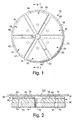
- An electrostatic wafer clamping apparatus includes a platen 10 and a clamping control circuit 12 for applying clamping voltages to the platen 10 when clamping of a workpiece is desired.
- the platen 10 includes a support plate, or a platen base 14, and six sector assemblies 20, 22, 24, 26, 28 and 30 mounted on an upper surface of platen base 14.
- the platen base 14 is generally circular and may have a central opening 18 for a wafer lift mechanism (not shown).
- Each of the sector assemblies includes a sector electrode located between an upper sector insulator and a lower sector insulator.
- Sector assemblies 20, 22, 24, 26, 28 and 30 include sector electrodes 40, 42, 44, 46, 48 and 50, respectively.
- Upper sector insulators 60, 62, 64, 66, 68 and 70 cover electrodes 40, 42, 44, 46, 48 and 50, respectively.
- the electrodes are preferably thin metal layers formed on the lower surfaces of the respective upper sector insulators.
- the electrodes 40, 42, 44, 46, 48 and 50 preferably have equal areas and are symmetrically disposed with respect to a center 72 of platen 10.
- the electrodes are electrically isolated from each other and, in a preferred embodiment, are sector-shaped as shown in FIG. 1.
- sector assembly 20 includes a lower sector insulator 80 and sector assembly 26 includes a lower sector insulator 86.
- the remaining sector assemblies have the same construction.
- the upper and lower sector insulators of each sector assembly overlap the edges of the respective electrodes to prevent contact between the electrodes and the wafer.
- a separate sector assembly including sector-shaped upper and lower sector insulators is fabricated for each electrode.
- the upper insulator or the lower insulator, or both may be formed as a circular disk. Multiple electrodes may be formed on the lower surface of the circular upper insulator. This configuration may be practical for relatively small platens.
- the platen base 14 and the lower sector insulators 80, 86, etc., are provided with aligned openings 90 and 92, respectively, underlying each of the electrodes.
- the openings 90 and 92 permit electrical connection to each of the electrodes.
- a semiconductor wafer 100 is shown in FIG. 2 positioned above clamping surface 76. When clamping voltages are applied to electrodes 40, 42, 44, 46, 48 and 50, the wafer 100 is electrostatically clamped in a fixed position against clamping surface 76.
- the upper sector insulators 60, 62, 64, 66, 68 and 70 are preferably a hard ceramic material that has high dielectric strength and high permittivity, and does not exhibit bulk polarization at the frequency and voltage used for clamping.
- Preferred materials include alumina, sapphire, silicon carbide and aluminum nitride.
- the upper sector insulators may, for example, have a thickness of about 0.20mm (0.008 inch) to permit reliable clamping with a voltage having a peak amplitude of about 1000 volts.
- the upper surfaces of the upper sector insulators are ground flat to within 0.025mm (0.001 inch).
- the electrodes 40, 42, 44, 46, 48 and 50 are preferably formed by depositing metal layers on the lower surfaces of the respective upper sector insulators 60, 62, 64, 66, 68 and 70.
- the electrodes comprise a conductive coating of niobium.
- the thickness of each electrode is typically on the order of about one micrometer.
- Other suitable conductive metal layers may be used within the scope of the invention. For example, titanium-molybdenum electrodes are described in the aforementioned patent no. 5,452,177.
- the lower sector insulators have sufficient thickness to provide structural rigidity and to electrically isolate the electrodes.
- the lower sector insulators are preferably fabricated of the same or a similar material as the upper sector insulators for matching of thermal expansion coefficients.
- the lower sector insulators are fabricated of alumina.
- the platen base 14 is typically fabricated of a metal such as aluminum.
- Each upper sector insulator having an electrode formed on its lower surface is bonded to the upper surface of the lower sector insulator, preferably using a thermoplastic tetrafluoroethylene adhesive 108 (Fig. 4), such as Teflon FEP bonding material.
- the clamping voltages applied to the electrodes of platen 10 are preferably bipolar square waves having six different phases (0°, 60°, 120°, 180°, 240° and 300° ).
- the phases of the voltages applied to electrodes on opposite sides of platen 10 are one-half cycle, or 180°, out of phase.
- the voltages applied to electrodes 40 and 46 are one-half cycle out of phase
- the voltages applied to electrodes 42 and 48 are one-half cycle out of phase
- the voltages applied to electrodes 44 and 50 are one-half cycle out of phase.
- the disclosed clamping apparatus provides reliable clamping and unclamping of wafers without requiring electrical contact to the wafer and without producing charging currents which could potentially damage the wafer.
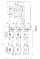
- FIG. 3 An example of a suitable clamping control circuit 12 is shown in FIG. 3.
- Square wave generators 110, 112 and 114 supply low voltage square waves to amplifiers 120, 122 and 124, respectively.
- the outputs of amplifiers 120, 122 and 124 are applied to high voltage inverter transformers 130, 132 and 134, respectively.
- the transformers 130, 132 and 134 produce output voltages that are 180°, or one-half cycle, out of phase.
- the outputs of transformer 130 on lines 140 and 142 are bipolar square waves that are one-half cycle out of phase.
- the outputs on lines 140 and 142 are connected to electrodes 46 and 40, respectively.
- the outputs of transformer 130 on lines 144 and 146 are bipolar square waves that arc one-half cycle out of phase and are shifted by 120° relative to the outputs of transformer 130.
- the outputs of transformer 132 on lines 144 and 146 are connected to electrodes 48 and 42, respectively.
- the outputs of transformer 134 on lines 148 and 150 are one-half cycle out of phase and are shifted by 240° relative to the outputs of transformer 130.
- the outputs of transformer 134 on lines 148 and 150 are connected to electrodes 50 and 44, respectively.
- This configuration provides six phase clamping of the wafer. Additional details regarding the clamping control circuit and the clamping voltages are provided in the aforementioned patent no. 4,452,177, which is hereby incorporated by reference.
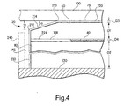
- FIG. 4 A partial cross-sectional view of an example of an implementation of the electrostatic wafer clamp of the invention is shown in FIG. 4. Like elements in FIGS. 1,2 and 4 have the same reference numerals. A portion of sector assembly 20 is shown. It will be understood that FIG. 4 is not drawn to scale in order to facilitate an understanding of the present invention. As indicated, electrode 40 is positioned between upper sector insulator 60 and lower sector insulator 80. Sector insulators 60 and 80 are secured together with adhesive 108. Electrode 40 is preferably spaced from a side 200 of sector assembly 20. In a preferred embodiment, electrode 40 is spaced from side 200 by about 2.54mm (0.1 inch).
- a periphery of upper sector insulator 60 is beveled to define a first blunt edge 210 that forms a boundary of clamping surface 76, and a second edge 212 that is spaced from the wafer 100.
- the beveled periphery defines a beveled surface 214 that forms a relatively shallow angle a with respect to the wafer 100 positioned on clamping surface 76.
- the periphery of each of the upper sector insulators 60, 62, 64, 66, 68 and 70 (FIG. 1) is beveled in this manner.
- the blunt edge 210 that forms the intersection between beveled surface 214 and clamping surface 76 is preferably blended and polished to form a smooth transition between these surfaces.
- the angle a is preferably less than about 10°, so that the beveled surface 214 has a very small slope relative to clamping surface 76.
- edge 212 may be relatively sharp, it is spaced from wafer by a spacing S 1 and does not normally contact wafer 100.
- the effect of the beveled periphery is a tapering of the clamping surface toward the edges of the sector assembly, with no sharp edge contacting wafer 100.
- the wafer contacts blunt edge 210, it contacts a relatively large surface so that forces are distributed. This reduces the amount of damage sustained by the wafer and thereby reduces the number of particles generated.
- the beveled surface 214 is relatively wide compared to the particle size. When the clamp is energized, free particles in the vacuum chamber are attracted to the platen edge by the electrostatic field. These particles tend to collect on the beveled surface 214 and in the vicinity of edge 212. The quantity of particles is determined by the quantity of free particles in the system.
- edges 210 and 212 are preferably rounded and polished to remove protruding grains of the dielectric material, typically alumina, which can be quite sharp and cause wafer damage.
- Such sharp protruding grains may not only damage the wafer, but also act as fulcrums on which the wafer pivots.
- the wafer rests on such protruding grains, allowing free space between the clamping surface and the wafer. This effectively adds another dielectric layer to the clamp and increases the distance between the electrode and the wafer, both of which reduce the clamping force. Due to variations in surface features and flatness of the wafers, no two wafers rest on the protruding grains in exactly the same manner. Consequently, the clamping force and the number of particles generated per wafer are likely to vary. The removal of these sharp protruding grains has been shown to produce a nine-fold decrease in clamping force variation and an over fifty-fold decrease in particle count variation.
- the upper sector insulator 60 is high purity (99.5%) alumina having a thickness D1 of about 0.20mm of about (0.008 inch).
- Lower sector insulator 80 may be lower purity alumina having a thickness D2 of about. 2.5mm (0.1 inch).
- Beveled surface 214 has a width of about 0.889mm (0.035 inch), and the angle a with respect to wafer 100 is about 5°. As a result, edge 212 is spaced from wafer 100 by spacing S1 on the order of about 0.101mm (0.004 inch), and the particles that accumulate at edge 212 are unlikely to contact wafer 100.
- Beveled surface 214 is preferably located outwardly of electrode 40 toward the side 200 of sector assembly 20. It will be understood that the above dimensions are given by way of example only and are in no way limiting as to the scope of the present invention.
- a low friction, high hardness dielectric coating 220 is applied to the upper surface of each of the upper sector insulators 60, 62, 64, 66, 68 and 70.
- the coating 220 is a diamond-like, amorphous carbon coating.
- Other suitable coating materials include silicon carbide and aluminum nitride.
- the coating preferably has a thickness D3 in a range of about 0.5 micrometer to about 5.0 micrometers, and more preferably has a thickness of about 1.5 micrometers.
- the coating 220 thereby defines the clamping surface 76 of the wafer clamp.
- the coating 220 preferably covers beveled surface 214 and side 200 of each of the sector assemblies.
- the carbon coating may be applied by conformal plasma induced vapor deposition, using known techniques.
- the coating provides a number of advantages. It lowers friction between the clamping surface 76 of the platen and wafer 100. Thus, if the wafer moves laterally relative to the clamping surface, features on the wafer tend to slide rather than break off and become particles.
- the coating provides a relatively hermetic seal over the grain structure of upper sector insulator 60 which, as noted above, is typically alumina. This means that particles are not ground into the grain structure, to be retained and later released. The brown staining that has been observed in the absence of the coating is not observed when the coating is utilized.
- the thickness of the coating increases the radius of sharp surface features on the platen by the thickness of the coating.
- the radii of surface features are increased by an order of magnitude relative to the diameter of the smallest and most numerous particles of concern in semiconductor wafer processing.
- the increase in radius of surface features produces an effectively higher negative rake angle between such features and the wafer, thus requiring more energy to break off a feature and create a particle.
- the wafer tends to slip up and slide over such features rather than being gouged.
- the coating provides a relatively hermetic seal of the sides of the sector assembly.
- the coating 220 covers side 200 of sector assembly 20 and seals interface 224 between upper sector insulator 60 and lower sector insulator 80. As indicated, the upper and lower sector insulators are fastened together with adhesive 108.
- the coating 220 prevents water vapor in the atmosphere, which may be present during storage and assembly, from entering the sides of the sector assembly.
- Water vapor entering the sector assembly along interface 224 may have the following undesirable effects: (1) the electrode 40 may corrode at its edge; (2) the Teflon adhesive layer may expand; (3) the edges of the sector assembly may deflect upwardly in the direction of wafer 100, potentially causing damage to wafers, due to the expansion at the edges caused by corrosion and water vapor absorption; and (4) sufficient water vapor may be retained such that a path from the electrode to ground is formed. In this case, the water boils instantly and the insulator cracks and is literally blown off the top of the sector assembly.
- electrode 40 preferably comprises niobium. Wetting of the niobium by the Teflon adhesive is superior to the wetting of prior art electrode materials. As a result, the elements of the sector assembly are more securely held together.
- the niobium electrode provides lower resistivity than prior art electrodes. The lower resistivity electrode compensates for electrical effects of carbon coating 220. The carbon coating functions to some degree as a dissipator of localized charges on the platen surface, because the carbon coating is somewhat more conductive than the alumina surface. As a result, the clamping force is somewhat reduced by the carbon coating. By providing niobium electrodes with lower resistivities, more charge is supplied to the clamping surface.
- the niobium electrodes are sputtered from a niobium source of 99% purity to a thickness D4 which achieves 0.13 ohms per square. Nitrogen may be added near the end of the process to form niobium nitride on the surface of the electrode and thereby provide low surface resistivity. It will be understood that different resistivities will be required for different geometries.
- the wafer When the electrostatic wafer clamp is energized, the wafer vibrates due to the forces resulting from the alternating electric fields.
- the magnitude of the vibration is believed to be sufficient to contribute to some extent to particle generation.
- the magnitudes of vibration have been measured to be less than 0.025mm (0.001 inch) on prior art electrostatic wafer clamps and thus do not affect the implant process directly. However, it is believed that a reduction in vibration will produce an improvement in particle performance.
- the sector assemblies in prior art wafer clamps are held to the platen base by a relatively rigid epoxy.
- the sector assemblies thus define a relatively stationary surface against which the wafer impacts during vibration.
- the rigid epoxy is replaced with a resilient, lower durometer adhesive 230 (FIG. 4).
- the platen base 14 is provided with sector shaped recesses to locate the sector assemblies during manufacturing.
- An outer lip 240 of each recess shown in phantom in FIG. 4, retains the sector assembly radially.
- a small space 242 is left between the lip 240 and the sector assembly. This space 242 acts as a particle reservoir.
- the electrostatic field of the wafer clamp attracts free particles and deposits them at and near the edge of the sector assembly, where they tend to fall into space 242 and accumulate. Particles also accumulate on lip 240.
- the lip of the platen base is removed or lowered so that it is spaced from the wafer by a greater distance than in prior art wafer clamps. Particles then have a lower probability of being deposited in the region of the lip and in the space between the lip and the sector assembly. Any particles that are deposited in this region are spaced farther from the wafer than in prior art wafer clamps.
- the periphery of the platen is easier to clean.
- the sector assemblies may be located relative to the platen base during assembly using a jig, as is known in the manufacturing art.
Claims (31)
- Dispositif de serrage électrostatique d'une pièce à traiter, comprenant :un ensemble formant plateau (10) définissant une surface de serrage électriquement isolante (76) pour recevoir une pièce à traiter (100), ledit ensemble formant plateau (10) comprenant des électrodes (40-50) situées au-dessous de et isolées électriquement par rapport à ladite surface de serrage (76), et une couche diélectrique (60-70) située entre lesdites électrodes (40-50) et ladite surface de serrage (76), ladite couche diélectrique (60-70) possédant une périphérie qui est biseautée (214) de manière à définir un premier bord émoussé (210) qui forme une limite de la surface de serrage (76) et un second bord (212), qui est distant de la pièce à traiter (100); etun circuit de commande de serrage (12) pour appliquer des tensions de serrage auxdites électrodes (40-50) pour réaliser le serrage électrostatique de la pièce à traiter (100) dans une position fixe sur ladite surface de serrage (76).
- Dispositif selon la revendication 1, dans lequel la périphérie biseautée (214) de ladite couche diélectrique (60-70) définit une surface biseautée qui fait un angle inférieur à environ 10 degrés par rapport à la pièce à traiter (100) disposée sur ladite surface de serrage (76).
- Dispositif selon la revendication 1 ou 2, dans lequel le second bord (212) est distant d'au moins environ 0,10 mm (0,004 pouce) de la pièce à traiter (100) sur ladite surface de serrage (76).
- Dispositif selon la revendication 1, 2 ou 3, dans lequel la périphérie biseautée (214) de ladite couche diélectrique (60-70) définit une surface biseautée qui est située à l'extérieur desdites électrodes (40-50).
- Dispositif de serrage électrostatique d'une pièce à traiter, comprenant :un ensemble formant plateau définissant une surface de serrage électriquement isolante (76) servant à recevoir une pièce à traiter (100), ledit ensemble formant plateau comprenant des électrodes (40-50) situées au-dessous de et électriquement isolées par rapport à ladite surface de serrage (76), une couche diélectrique relativement épaisse (60-70) entre chacune desdites électrodes (40-50) et ladite surface de serrage (76) et un revêtement diélectrique relativement mince à faible coefficient de frottement et de grande dureté (220) recouvrant ladite couche diélectrique (60-70) et formant ladite surface de serrage (76), ledit revêtement diélectrique (220) comprenant du carbone amorphe, et ledit revêtement diélectrique (220) possédant une épaisseur dans une gamme allant d'environ 0,5 micromètre à environ 5,0 micromètre; etun circuit de commande de serrage (12) pour appliquer des tensions de serrage auxdites électrodes (40-50) pour réaliser le serrage électrostatique de la pièce à traiter (100) dans une position fixe sur ladite surface de serrage (76).
- Dispositif selon l'une quelconque des revendications précédentes, dans lequel ladite couche diélectrique (60-70) comprend un matériau choisi dans le groupe comprenant de l'alumine, du carbure de silicium et du nitrure d'aluminium.
- Dispositif selon l'une quelconque des revendications précédentes, dans lequel ladite couche diélectrique (60-70) comprend de l'alumine.
- Dispositif selon la revendication 7, considérée comme dépendante de la revendication 1, 2, 3 ou 4, dans lequel ledit ensemble formant plateau comprend en outre un revêtement diélectrique à faible coefficient de frottement et de grande dureté (220) recouvrant ladite alumine et définissant ladite surface de serrage (76).
- Dispositif selon la revendication 7, considérée comme dépendante de la revendication 1, 2, 3 ou 4, dans lequel ledit ensemble formant plateau comprend en outre un revêtement de carbone amorphe analogue au diamant, recouvrant ladite alumine et définissant ladite surface de serrage.
- Dispositif selon la revendication 9, dans lequel ledit revêtement de carbone possède une épaisseur qui se situe dans la gamme comprise entre environ 0,5 micromètre et environ 5,0 micromètres.
- Dispositif selon la revendication 9 ou 10, dans lequel ladite couche diélectrique (60-70) inclut un côté adjacent à ladite surface de serrage (76), dans lequel ledit revêtement de carbone recouvre le côté de ladite couche diélectrique (60-70).
- Dispositif selon l'une quelconque des revendications précédentes, dans lequel ladite couche diélectrique (60-70) possède une épaisseur égale à plusieurs multiples de 0,0254 mm (plusieurs millièmes de pouce).
- Dispositif selon l'une quelconque des revendications 5 à 12, dans lequel ladite couche diélectrique (60-70) comprend un côté adjacent à ladite surface de serrage (76), et dans lequel ledit revêtement diélectrique (220) recouvre ledit côté.
- Dispositif selon l'une quelconque des revendications 5 à 13, dans lequel ladite couche diélectrique (60-70) possède une périphérie (214) qui est biseautée de manière à définir un premier bord émoussé (210) qui forme une limite de la surface de serrage (76), et un second bord (212) qui est distant de la pièce à traiter (100).
- Dispositif selon la revendication 14, dans lequel ladite périphérie biseautée (214) définit une surface biseautée qui fait un angle inférieur à environ 10 degrés par rapport à la pièce à traiter (100) positionnée sur ladite surface de serrage (76).
- Dispositif selon la revendication 15, dans lequel ladite surface biseautée est située à l'extérieur desdites électrodes (40-50).
- Dispositif de serrage électrostatique d'une pastille semiconductrice comprenant :un plateau (10) comportant une pluralité d'ensembles en forme de secteurs (20-30) montés sur une base (14) du plateau, lesdits ensembles formant segments (20-30) définissant une surface de serrage essentiellement circulaire et électriquement isolante (76) servant à recevoir une pastille semiconductrice (100), chacun desdits ensembles en forme de secteurs (20-30) comprenant une électrode conductrice (40-50) située au-dessous et isolée électriquement de ladite surface de serrage (76), une couche diélectrique supérieure (60-70) entre ladite électrode (40-50) et ladite surface de serrage (76), et une couche diélectrique inférieure (80) entre ladite électrode (40-50) et ladite base (14) du plateau, ladite couche diélectrique supérieure (60-70) possédant une périphérie (214) qui est biseautée de manière à définir un premier bord émoussé (210) qui forme une limite de la surface de serrage (76), et un second bord. (212), qui est distant de la pastille semiconductrice (100); etun circuit de commande de serrage (12) servant à appliquer des tensions de serrage auxdites électrodes (40-50) pour réaliser le serrage électrostatique de la pastille semiconductrice (100) dans une position fixe sur ladite surface de serrage (76).
- Dispositif de serrage électrostatique selon la revendication 17, dans lequel la périphérie biseautée (214) de ladite couche diélectrique supérieure (60-70) définit une surface biseautée qui fait un angle inférieur à environ 10 degrés par rapport à la pastille semiconductrice (100) disposée sur ladite surface de serrage (76).
- Dispositif de serrage électrostatique selon la revendication 17 ou 18, dans lequel ledit second bord (212) est distant de la pastille semiconductrice (100) sur ladite surface de serrage (76), et ce d'au moins environ 0,10 mm (0,004 pouce).
- Dispositif de serrage électrostatique selon la revendication 17, 18 ou 19, dans lequel la périphérie biseautée (214) de ladite couche diélectrique supérieure (60-70) définit une surface biseautée qui est située à l'extérieur desdites électrodes (40-50).
- Dispositif de serrage électrostatique selon la revendication 17, 18, 19 ou 20, dans lequel ladite couche diélectrique supérieure (60-70) comprend de l'alumine.
- Dispositif de serrage électrostatique selon la revendication 21, dans lequel chacun desdits ensembles formant secteurs (20-30) comprend en outre un revêtement de carbone amorphe semblable au diamant (220) qui chevauche ladite couche diélectrique supérieure (60-70) et définit ladite surface de serrage (76).
- Dispositif de serrage électrostatique selon la revendication 22, dans lequel ledit revêtement de carbone (220) possède une épaisseur située dans une gamme comprise entre environ 0,5 micromètre et environ 5,0 micromètres.
- Dispositif de serrage électrostatique selon la revendication 22 ou 23, dans laquelle chacun desdits ensembles formant secteurs (20-30) inclut un côté adjacent à ladite surface de serrage (76) et dans lequel ledit revêtement de carbone (220) recouvre le côté desdits ensembles formant secteurs (20-30).
- Dispositif de serrage électrostatique selon la revendication 22, 23 ou 24, dans lequel ledit revêtement en carbone possède une épaisseur d'environ 1,5 micromètre.
- Dispositif de serrage électrostatique selon la revendication 18, dans lequel ladite surface biseautée (214) fait un angle d'environ 5 degrés par rapport à la pastille semiconductrice (100) positionnée sur ladite surface de serrage (76).
- Dispositif de serrage électrostatique selon la revendication 26, dans lequel ledit bord émoussé (210) est uniformisé et poli de manière à former une transition douce entre ladite surface biseautée (214) et ladite surface de serrage (76).
- Dispositif de serrage électrostatique selon l'une quelconque des revendications 17 à 27, dans lequel chacun desdits ensembles formant secteurs (20-30) est fixé à ladite base (14) du plateau à l'aide d'un adhésif de faible dureté (203).
- Dispositif de serrage électrostatique selon l'une quelconque des revendications 17 à 28, dans lequel ladite base (14) du plateau est configurée de manière à éviter des renfoncements qui. pourraient éventuellement accumuler des particules.
- Dispositif de serrage électrostatique selon l'une quelconque des revendications précédentes, dans lequel lesdites électrodes (40-50) comprennent du niobium.
- Dispositif de serrage électrostatique d'une pastille semiconductrice comprenant :un plateau (10) comportant une pluralité d'ensembles formant secteurs (20-30) montés sur une base (14) du plateau, lesdits ensembles formant secteurs (20-30) définissant une surface de serrage essentiellement circulaire et électriquement isolante (76) servant à recevoir une pastille semiconductrice (100), chacun desdits ensembles formant secteurs (20-30) comprenant une électrode conductrice (40-50) située au-dessous et isolée électriquement de ladite surface de serrage (76), une couche diélectrique supérieure relativement épaisse (60-70) située entre chacune desdites électrodes (40-50) et ladite surface de serrage (76), un revêtement relativement mince à faible coefficient de frottement et de grande dureté (220) recouvrant ladite couche diélectrique supérieure (60-70) et formant ladite surface de serrage (76), et une couche diélectrique inférieure (80) située entre ladite électrode (40-50) et ladite base (14) du plateau, ledit revêtement diélectrique (220) comprenant du carbone amorphe, et dans lequel ledit revêtement diélectrique (220) possède une épaisseur dans une gamme comprise entre environ 0,5 micromètre et environ 5,0 micromètres; etun circuit de commande de serrage (12) servant à appliquer des tensions de serrage auxdites électrodes (40-50) pour réaliser le serrage électrostatique de la pastille semiconductrice (100) dans une position fixe sur ladite surface de serrage (76).
Applications Claiming Priority (3)
| Application Number | Priority Date | Filing Date | Title |
|---|---|---|---|
| US58944 | 1987-06-05 | ||
| US09/058,944 US5969934A (en) | 1998-04-10 | 1998-04-10 | Electrostatic wafer clamp having low particulate contamination of wafers |
| PCT/US1999/007752 WO1999053603A1 (fr) | 1998-04-10 | 1999-04-08 | Pince electrostatique pour plaquettes a faible contamination particulaire des plaquettes |
Publications (2)
| Publication Number | Publication Date |
|---|---|
| EP1070381A1 EP1070381A1 (fr) | 2001-01-24 |
| EP1070381B1 true EP1070381B1 (fr) | 2003-01-02 |
Family
ID=22019869
Family Applications (1)
| Application Number | Title | Priority Date | Filing Date |
|---|---|---|---|
| EP99916529A Expired - Lifetime EP1070381B1 (fr) | 1998-04-10 | 1999-04-08 | Pince electrostatique pour plaquettes a faible contamination particulaire des plaquettes |
Country Status (7)
| Country | Link |
|---|---|
| US (1) | US5969934A (fr) |
| EP (1) | EP1070381B1 (fr) |
| JP (1) | JP2002511662A (fr) |
| KR (1) | KR100625712B1 (fr) |
| DE (1) | DE69904709T2 (fr) |
| TW (1) | TW410414B (fr) |
| WO (1) | WO1999053603A1 (fr) |
Families Citing this family (39)
| Publication number | Priority date | Publication date | Assignee | Title |
|---|---|---|---|---|
| KR100308209B1 (ko) * | 1998-06-20 | 2001-11-30 | 윤종용 | 리플로우공정을 위한 히터 어셈블리의 클램프 |
| US6839217B1 (en) | 1999-10-01 | 2005-01-04 | Varian Semiconductor Equipment Associates, Inc. | Surface structure and method of making, and electrostatic wafer clamp incorporating surface structure |
| US6362946B1 (en) | 1999-11-02 | 2002-03-26 | Varian Semiconductor Equipment Associates, Inc. | Electrostatic wafer clamp having electrostatic seal for retaining gas |
| US6538873B1 (en) | 1999-11-02 | 2003-03-25 | Varian Semiconductor Equipment Associates, Inc. | Active electrostatic seal and electrostatic vacuum pump |
| JP5165817B2 (ja) * | 2000-03-31 | 2013-03-21 | ラム リサーチ コーポレーション | 静電チャック及びその製造方法 |
| US20030107865A1 (en) * | 2000-12-11 | 2003-06-12 | Shinsuke Masuda | Wafer handling apparatus and method of manufacturing the same |
| KR20020046214A (ko) * | 2000-12-11 | 2002-06-20 | 어드밴스드 세라믹스 인터내셔날 코포레이션 | 정전척 및 그 제조방법 |
| US6528767B2 (en) * | 2001-05-22 | 2003-03-04 | Applied Materials, Inc. | Pre-heating and load lock pedestal material for high temperature CVD liquid crystal and flat panel display applications |
| JP2002359281A (ja) * | 2001-06-01 | 2002-12-13 | Ngk Spark Plug Co Ltd | セラミックヒータ及びその製造方法 |
| US6483690B1 (en) | 2001-06-28 | 2002-11-19 | Lam Research Corporation | Ceramic electrostatic chuck assembly and method of making |
| US6805137B2 (en) | 2001-08-27 | 2004-10-19 | Applied Materials, Inc. | Method for removing contamination particles from substrates |
| US6779226B2 (en) | 2001-08-27 | 2004-08-24 | Applied Materials, Inc. | Factory interface particle removal platform |
| US20030037800A1 (en) * | 2001-08-27 | 2003-02-27 | Applied Materials, Inc. | Method for removing contamination particles from substrate processing chambers |
| US6725564B2 (en) | 2001-08-27 | 2004-04-27 | Applied Materials, Inc. | Processing platform with integrated particle removal system |
| US6878636B2 (en) * | 2001-08-27 | 2005-04-12 | Applied Materials, Inc. | Method for enhancing substrate processing |
| US6684523B2 (en) | 2001-08-27 | 2004-02-03 | Applied Materials, Inc. | Particle removal apparatus |
| US20030037801A1 (en) * | 2001-08-27 | 2003-02-27 | Applied Materials, Inc. | Method for increasing the efficiency of substrate processing chamber contamination detection |
| JP2003269549A (ja) * | 2002-03-19 | 2003-09-25 | Tsubakimoto Chain Co | 耐摩耗性チェーン |
| US6660665B2 (en) * | 2002-05-01 | 2003-12-09 | Japan Fine Ceramics Center | Platen for electrostatic wafer clamping apparatus |
| US20040055709A1 (en) * | 2002-09-19 | 2004-03-25 | Applied Materials, Inc. | Electrostatic chuck having a low level of particle generation and method of fabricating same |
| US20040066601A1 (en) * | 2002-10-04 | 2004-04-08 | Varian Semiconductor Equipment Associates, Inc. | Electrode configuration for retaining cooling gas on electrostatic wafer clamp |
| US20040226516A1 (en) * | 2003-05-13 | 2004-11-18 | Daniel Timothy J. | Wafer pedestal cover |
| TWI254188B (en) * | 2003-07-23 | 2006-05-01 | Asml Netherlands Bv | Lithographic projection apparatus and article holder therefor |
| US6946403B2 (en) * | 2003-10-28 | 2005-09-20 | Axcelis Technologies, Inc. | Method of making a MEMS electrostatic chuck |
| US7824498B2 (en) * | 2004-02-24 | 2010-11-02 | Applied Materials, Inc. | Coating for reducing contamination of substrates during processing |
| DE202005011367U1 (de) | 2005-07-18 | 2005-09-29 | Retzlaff, Udo, Dr. | Transfer-ESC auf Wafer-Basis |
| CN100362644C (zh) * | 2005-12-07 | 2008-01-16 | 北京北方微电子基地设备工艺研究中心有限责任公司 | 静电卡盘 |
| US20070181420A1 (en) * | 2006-02-07 | 2007-08-09 | Ming-Tung Wang | Wafer stage having an encapsulated central pedestal plate |
| MY166000A (en) * | 2007-12-19 | 2018-05-21 | Lam Res Corp | A composite showerhead electrode assembly for a plasma processing apparatus |
| WO2009078923A2 (fr) | 2007-12-19 | 2009-06-25 | Lam Research Corporation | Film adhésif pour appareil de traitement sous vide à semi-conducteurs |
| TWI475594B (zh) * | 2008-05-19 | 2015-03-01 | Entegris Inc | 靜電夾頭 |
| US8169769B2 (en) * | 2008-09-11 | 2012-05-01 | Tel Epion Inc. | Electrostatic chuck power supply |
| US7948734B2 (en) * | 2008-09-11 | 2011-05-24 | Tel Epion Inc. | Electrostatic chuck power supply |
| US8861170B2 (en) | 2009-05-15 | 2014-10-14 | Entegris, Inc. | Electrostatic chuck with photo-patternable soft protrusion contact surface |
| SG10201407637TA (en) * | 2009-11-30 | 2015-01-29 | Lam Res Corp | An electrostatic chuck with an angled sidewall |
| US8840754B2 (en) * | 2010-09-17 | 2014-09-23 | Lam Research Corporation | Polar regions for electrostatic de-chucking with lift pins |
| US9633885B2 (en) * | 2014-02-12 | 2017-04-25 | Axcelis Technologies, Inc. | Variable electrode pattern for versatile electrostatic clamp operation |
| WO2016135565A1 (fr) | 2015-02-23 | 2016-09-01 | M Cubed Technologies, Inc. | Électrode à film pour mandrin électrostatique |
| SG11201906817TA (en) * | 2017-01-27 | 2019-08-27 | Ultratech Inc | Chuck systems and methods having enhanced electrical isolation for substrate-biased ald |
Family Cites Families (54)
| Publication number | Priority date | Publication date | Assignee | Title |
|---|---|---|---|---|
| GB1443215A (en) * | 1973-11-07 | 1976-07-21 | Mullard Ltd | Electrostatically clamping a semiconductor wafer during device manufacture |
| US4184188A (en) * | 1978-01-16 | 1980-01-15 | Veeco Instruments Inc. | Substrate clamping technique in IC fabrication processes |
| US4176365A (en) * | 1978-05-08 | 1979-11-27 | Sperry Rand Corporation | Josephson tunnel junction device with hydrogenated amorphous silicon, germanium or silicon-germanium alloy tunneling barrier |
| US4384918A (en) * | 1980-09-30 | 1983-05-24 | Fujitsu Limited | Method and apparatus for dry etching and electrostatic chucking device used therein |
| GB2106325A (en) * | 1981-09-14 | 1983-04-07 | Philips Electronic Associated | Electrostatic chuck |
| US4412133A (en) * | 1982-01-05 | 1983-10-25 | The Perkin-Elmer Corp. | Electrostatic cassette |
| JPS6059104B2 (ja) * | 1982-02-03 | 1985-12-23 | 株式会社東芝 | 静電チヤツク板 |
| US4457359A (en) * | 1982-05-25 | 1984-07-03 | Varian Associates, Inc. | Apparatus for gas-assisted, solid-to-solid thermal transfer with a semiconductor wafer |
| JPS5929435A (ja) * | 1982-08-11 | 1984-02-16 | Hitachi Ltd | 試料支持装置 |
| GB2154365A (en) * | 1984-02-10 | 1985-09-04 | Philips Electronic Associated | Loading semiconductor wafers on an electrostatic chuck |
| GB2147459A (en) * | 1983-09-30 | 1985-05-09 | Philips Electronic Associated | Electrostatic chuck for semiconductor wafers |
| US4692836A (en) * | 1983-10-31 | 1987-09-08 | Toshiba Kikai Kabushiki Kaisha | Electrostatic chucks |
| US4603466A (en) * | 1984-02-17 | 1986-08-05 | Gca Corporation | Wafer chuck |
| JPS6131636U (ja) * | 1984-07-31 | 1986-02-26 | 株式会社 徳田製作所 | 静電チヤツク |
| US4724510A (en) * | 1986-12-12 | 1988-02-09 | Tegal Corporation | Electrostatic wafer clamp |
| JP2678381B2 (ja) * | 1987-05-06 | 1997-11-17 | ユニサーチ・リミテッド | 交流電界励振を利用した静電チャック |
| US4938992A (en) * | 1988-01-07 | 1990-07-03 | Varian Associates, Inc. | Methods for thermal transfer with a semiconductor |
| US4832781A (en) * | 1988-01-07 | 1989-05-23 | Varian Associates, Inc. | Methods and apparatus for thermal transfer with a semiconductor wafer in vacuum |
| JPH0279481A (ja) * | 1988-09-16 | 1990-03-20 | Nippon Telegr & Teleph Corp <Ntt> | 磁束量子論理素子 |
| US5179498A (en) * | 1990-05-17 | 1993-01-12 | Tokyo Electron Limited | Electrostatic chuck device |
| US5452177A (en) * | 1990-06-08 | 1995-09-19 | Varian Associates, Inc. | Electrostatic wafer clamp |
| JPH04132239A (ja) * | 1990-09-21 | 1992-05-06 | Fujitsu Ltd | ウエハーチャック |
| US5166856A (en) * | 1991-01-31 | 1992-11-24 | International Business Machines Corporation | Electrostatic chuck with diamond coating |
| JPH04371579A (ja) * | 1991-06-19 | 1992-12-24 | Ulvac Japan Ltd | 静電吸着装置 |
| JPH05114119A (ja) * | 1991-10-21 | 1993-05-07 | Fujitsu Ltd | 磁気抵抗効果型磁気ヘツド |
| US5275683A (en) * | 1991-10-24 | 1994-01-04 | Tokyo Electron Limited | Mount for supporting substrates and plasma processing apparatus using the same |
| US5315473A (en) * | 1992-01-21 | 1994-05-24 | Applied Materials, Inc. | Isolated electrostatic chuck and excitation method |
| WO1994011944A1 (fr) * | 1992-11-06 | 1994-05-26 | Varian Associates, Inc. | Dispositif de serrage electrostatique de tranche |
| US5460684A (en) * | 1992-12-04 | 1995-10-24 | Tokyo Electron Limited | Stage having electrostatic chuck and plasma processing apparatus using same |
| US5444597A (en) * | 1993-01-15 | 1995-08-22 | Blake; Julian G. | Wafer release method and apparatus |
| US5436790A (en) * | 1993-01-15 | 1995-07-25 | Eaton Corporation | Wafer sensing and clamping monitor |
| US5345999A (en) * | 1993-03-17 | 1994-09-13 | Applied Materials, Inc. | Method and apparatus for cooling semiconductor wafers |
| US5384682A (en) * | 1993-03-22 | 1995-01-24 | Toto Ltd. | Electrostatic chuck |
| JPH06326175A (ja) * | 1993-04-22 | 1994-11-25 | Applied Materials Inc | 集積回路処理装置において使用されるウエハサポートの誘電材への保護被覆とその形成方法 |
| JP2851766B2 (ja) * | 1993-04-28 | 1999-01-27 | 京セラ株式会社 | 静電チャック |
| US5636098A (en) * | 1994-01-06 | 1997-06-03 | Applied Materials, Inc. | Barrier seal for electrostatic chuck |
| US5631803A (en) * | 1995-01-06 | 1997-05-20 | Applied Materials, Inc. | Erosion resistant electrostatic chuck with improved cooling system |
| EP0669644B1 (fr) * | 1994-02-28 | 1997-08-20 | Applied Materials, Inc. | Support électrostatique |
| US5535090A (en) * | 1994-03-03 | 1996-07-09 | Sherman; Arthur | Electrostatic chuck |
| US5459632A (en) * | 1994-03-07 | 1995-10-17 | Applied Materials, Inc. | Releasing a workpiece from an electrostatic chuck |
| US5474614A (en) * | 1994-06-10 | 1995-12-12 | Texas Instruments Incorporated | Method and apparatus for releasing a semiconductor wafer from an electrostatic clamp |
| US5646814A (en) * | 1994-07-15 | 1997-07-08 | Applied Materials, Inc. | Multi-electrode electrostatic chuck |
| US5606485A (en) * | 1994-07-18 | 1997-02-25 | Applied Materials, Inc. | Electrostatic chuck having improved erosion resistance |
| US5528451A (en) * | 1994-11-02 | 1996-06-18 | Applied Materials, Inc | Erosion resistant electrostatic chuck |
| JPH0945758A (ja) * | 1995-07-31 | 1997-02-14 | Kyocera Corp | 吸着装置 |
| JPH0945753A (ja) * | 1995-07-28 | 1997-02-14 | Kyocera Corp | 物品保持装置 |
| US5644467A (en) * | 1995-09-28 | 1997-07-01 | Applied Materials, Inc. | Method and structure for improving gas breakdown resistance and reducing the potential of arcing in a electrostatic chuck |
| US5697427A (en) * | 1995-12-22 | 1997-12-16 | Applied Materials, Inc. | Apparatus and method for cooling a substrate |
| US5900062A (en) * | 1995-12-28 | 1999-05-04 | Applied Materials, Inc. | Lift pin for dechucking substrates |
| JPH09283605A (ja) * | 1996-04-09 | 1997-10-31 | Canon Inc | 基板の吸着保持装置およびその製造方法 |
| US5825607A (en) * | 1996-05-08 | 1998-10-20 | Applied Materials, Inc. | Insulated wafer spacing mask for a substrate support chuck and method of fabricating same |
| TW303505B (en) * | 1996-05-08 | 1997-04-21 | Applied Materials Inc | Substrate support chuck having a contaminant containment layer and method of fabricating same |
| US5754391A (en) * | 1996-05-17 | 1998-05-19 | Saphikon Inc. | Electrostatic chuck |
| US5812362A (en) * | 1996-06-14 | 1998-09-22 | Applied Materials, Inc. | Method and apparatus for the use of diamond films as dielectric coatings on electrostatic chucks |
-
1998
- 1998-04-10 US US09/058,944 patent/US5969934A/en not_active Expired - Lifetime
-
1999
- 1999-04-08 JP JP2000544055A patent/JP2002511662A/ja active Pending
- 1999-04-08 DE DE69904709T patent/DE69904709T2/de not_active Expired - Fee Related
- 1999-04-08 EP EP99916529A patent/EP1070381B1/fr not_active Expired - Lifetime
- 1999-04-08 WO PCT/US1999/007752 patent/WO1999053603A1/fr active IP Right Grant
- 1999-04-08 KR KR1020007011266A patent/KR100625712B1/ko not_active IP Right Cessation
- 1999-04-09 TW TW088105658A patent/TW410414B/zh not_active IP Right Cessation
Also Published As
| Publication number | Publication date |
|---|---|
| US5969934A (en) | 1999-10-19 |
| TW410414B (en) | 2000-11-01 |
| DE69904709T2 (de) | 2003-11-13 |
| EP1070381A1 (fr) | 2001-01-24 |
| KR100625712B1 (ko) | 2006-09-20 |
| KR20010042592A (ko) | 2001-05-25 |
| WO1999053603A1 (fr) | 1999-10-21 |
| DE69904709D1 (de) | 2003-02-06 |
| JP2002511662A (ja) | 2002-04-16 |
Similar Documents
| Publication | Publication Date | Title |
|---|---|---|
| EP1070381B1 (fr) | Pince electrostatique pour plaquettes a faible contamination particulaire des plaquettes | |
| US6388861B1 (en) | Electrostatic wafer clamp | |
| KR101896127B1 (ko) | 고 전도성 정전 척 | |
| US5880924A (en) | Electrostatic chuck capable of rapidly dechucking a substrate | |
| US7848077B2 (en) | Electrostatic chuck device | |
| EP0541400B1 (fr) | Support électrostatique anti-adhésif pour un environnement à basse pression | |
| US6104596A (en) | Apparatus for retaining a subtrate in a semiconductor wafer processing system and a method of fabricating same | |
| JP3292270B2 (ja) | 静電吸着装置 | |
| US6839217B1 (en) | Surface structure and method of making, and electrostatic wafer clamp incorporating surface structure | |
| EP0620953B1 (fr) | Dispositif de serrage electrostatique de tranche | |
| JP4338376B2 (ja) | 静電チャック装置 | |
| EP1224687A2 (fr) | Structure superficielle et procede de fabrication correspondant, et fixation de plaquette electrostatique incorporant une structure superficielle | |
| JP2004253402A (ja) | 静電チャック装置 | |
| EP0460954B1 (fr) | Serrage de la pièce à usiner | |
| KR20230008343A (ko) | 정전척 캐리어 | |
| KR20070117747A (ko) | 스퍼터링장치 |
Legal Events
| Date | Code | Title | Description |
|---|---|---|---|
| PUAI | Public reference made under article 153(3) epc to a published international application that has entered the european phase |
Free format text: ORIGINAL CODE: 0009012 |
|
| 17P | Request for examination filed |
Effective date: 20001013 |
|
| AK | Designated contracting states |
Kind code of ref document: A1 Designated state(s): DE FR GB IE IT |
|
| GRAG | Despatch of communication of intention to grant |
Free format text: ORIGINAL CODE: EPIDOS AGRA |
|
| 17Q | First examination report despatched |
Effective date: 20020315 |
|
| GRAG | Despatch of communication of intention to grant |
Free format text: ORIGINAL CODE: EPIDOS AGRA |
|
| GRAH | Despatch of communication of intention to grant a patent |
Free format text: ORIGINAL CODE: EPIDOS IGRA |
|
| GRAH | Despatch of communication of intention to grant a patent |
Free format text: ORIGINAL CODE: EPIDOS IGRA |
|
| GRAA | (expected) grant |
Free format text: ORIGINAL CODE: 0009210 |
|
| AK | Designated contracting states |
Kind code of ref document: B1 Designated state(s): DE FR GB IE IT |
|
| REG | Reference to a national code |
Ref country code: GB Ref legal event code: FG4D Free format text: 20030102 |
|
| REG | Reference to a national code |
Ref country code: IE Ref legal event code: FG4D |
|
| REF | Corresponds to: |
Ref document number: 69904709 Country of ref document: DE Date of ref document: 20030206 Kind code of ref document: P |
|
| ET | Fr: translation filed | ||
| PLBE | No opposition filed within time limit |
Free format text: ORIGINAL CODE: 0009261 |
|
| STAA | Information on the status of an ep patent application or granted ep patent |
Free format text: STATUS: NO OPPOSITION FILED WITHIN TIME LIMIT |
|
| 26N | No opposition filed |
Effective date: 20031003 |
|
| PGFP | Annual fee paid to national office [announced via postgrant information from national office to epo] |
Ref country code: GB Payment date: 20050330 Year of fee payment: 7 |
|
| PGFP | Annual fee paid to national office [announced via postgrant information from national office to epo] |
Ref country code: FR Payment date: 20050418 Year of fee payment: 7 |
|
| PGFP | Annual fee paid to national office [announced via postgrant information from national office to epo] |
Ref country code: IE Payment date: 20050425 Year of fee payment: 7 |
|
| PGFP | Annual fee paid to national office [announced via postgrant information from national office to epo] |
Ref country code: DE Payment date: 20050531 Year of fee payment: 7 |
|
| PG25 | Lapsed in a contracting state [announced via postgrant information from national office to epo] |
Ref country code: GB Free format text: LAPSE BECAUSE OF NON-PAYMENT OF DUE FEES Effective date: 20060408 |
|
| PG25 | Lapsed in a contracting state [announced via postgrant information from national office to epo] |
Ref country code: IE Free format text: LAPSE BECAUSE OF NON-PAYMENT OF DUE FEES Effective date: 20060410 |
|
| PG25 | Lapsed in a contracting state [announced via postgrant information from national office to epo] |
Ref country code: DE Free format text: LAPSE BECAUSE OF NON-PAYMENT OF DUE FEES Effective date: 20061101 |
|
| GBPC | Gb: european patent ceased through non-payment of renewal fee |
Effective date: 20060408 |
|
| REG | Reference to a national code |
Ref country code: IE Ref legal event code: MM4A |
|
| REG | Reference to a national code |
Ref country code: FR Ref legal event code: ST Effective date: 20061230 |
|
| PGFP | Annual fee paid to national office [announced via postgrant information from national office to epo] |
Ref country code: IT Payment date: 20070519 Year of fee payment: 9 |
|
| PG25 | Lapsed in a contracting state [announced via postgrant information from national office to epo] |
Ref country code: FR Free format text: LAPSE BECAUSE OF NON-PAYMENT OF DUE FEES Effective date: 20060502 |
|
| PG25 | Lapsed in a contracting state [announced via postgrant information from national office to epo] |
Ref country code: IT Free format text: LAPSE BECAUSE OF NON-PAYMENT OF DUE FEES Effective date: 20080408 |