EP1069781A2 - Videosignal-Aufnahme- und/oder -Wiedergabeanlage und -Verfahren, und Bildaufnahmeanlage - Google Patents
Videosignal-Aufnahme- und/oder -Wiedergabeanlage und -Verfahren, und Bildaufnahmeanlage Download PDFInfo
- Publication number
- EP1069781A2 EP1069781A2 EP00305879A EP00305879A EP1069781A2 EP 1069781 A2 EP1069781 A2 EP 1069781A2 EP 00305879 A EP00305879 A EP 00305879A EP 00305879 A EP00305879 A EP 00305879A EP 1069781 A2 EP1069781 A2 EP 1069781A2
- Authority
- EP
- European Patent Office
- Prior art keywords
- data rate
- recording
- video signal
- signal
- reproducing
- Prior art date
- Legal status (The legal status is an assumption and is not a legal conclusion. Google has not performed a legal analysis and makes no representation as to the accuracy of the status listed.)
- Granted
Links
Images

Classifications
-
- H—ELECTRICITY
- H04—ELECTRIC COMMUNICATION TECHNIQUE
- H04N—PICTORIAL COMMUNICATION, e.g. TELEVISION
- H04N5/00—Details of television systems
- H04N5/76—Television signal recording
- H04N5/765—Interface circuits between an apparatus for recording and another apparatus
- H04N5/77—Interface circuits between an apparatus for recording and another apparatus between a recording apparatus and a television camera
- H04N5/772—Interface circuits between an apparatus for recording and another apparatus between a recording apparatus and a television camera the recording apparatus and the television camera being placed in the same enclosure
-
- H—ELECTRICITY
- H04—ELECTRIC COMMUNICATION TECHNIQUE
- H04N—PICTORIAL COMMUNICATION, e.g. TELEVISION
- H04N11/00—Colour television systems
- H04N11/06—Transmission systems characterised by the manner in which the individual colour picture signal components are combined
- H04N11/20—Conversion of the manner in which the individual colour picture signal components are combined, e.g. conversion of colour television standards
-
- H—ELECTRICITY
- H04—ELECTRIC COMMUNICATION TECHNIQUE
- H04N—PICTORIAL COMMUNICATION, e.g. TELEVISION
- H04N7/00—Television systems
- H04N7/01—Conversion of standards, e.g. involving analogue television standards or digital television standards processed at pixel level
- H04N7/0127—Conversion of standards, e.g. involving analogue television standards or digital television standards processed at pixel level by changing the field or frame frequency of the incoming video signal, e.g. frame rate converter
- H04N7/013—Conversion of standards, e.g. involving analogue television standards or digital television standards processed at pixel level by changing the field or frame frequency of the incoming video signal, e.g. frame rate converter the incoming video signal comprising different parts having originally different frame rate, e.g. video and graphics
-
- H—ELECTRICITY
- H04—ELECTRIC COMMUNICATION TECHNIQUE
- H04N—PICTORIAL COMMUNICATION, e.g. TELEVISION
- H04N9/00—Details of colour television systems
- H04N9/79—Processing of colour television signals in connection with recording
- H04N9/7921—Processing of colour television signals in connection with recording for more than one processing mode
- H04N9/7925—Processing of colour television signals in connection with recording for more than one processing mode for more than one standard
-
- H—ELECTRICITY
- H04—ELECTRIC COMMUNICATION TECHNIQUE
- H04N—PICTORIAL COMMUNICATION, e.g. TELEVISION
- H04N5/00—Details of television systems
- H04N5/76—Television signal recording
- H04N5/907—Television signal recording using static stores, e.g. storage tubes or semiconductor memories
-
- H—ELECTRICITY
- H04—ELECTRIC COMMUNICATION TECHNIQUE
- H04N—PICTORIAL COMMUNICATION, e.g. TELEVISION
- H04N9/00—Details of colour television systems
- H04N9/79—Processing of colour television signals in connection with recording
- H04N9/7921—Processing of colour television signals in connection with recording for more than one processing mode
Definitions
- the present invention relates to a recording and/or reproducing technique suited for use in a digital camcorder or the like.
- the present invention is particularly suitable for allowing a still image signal recorded at, for example, a different data rate and supplied from a semiconductor memory or the like, to be captured at the data rate of, for example, a video signal.
- a recording and reproducing apparatus into which a semiconductor memory as well as a magnetic recording medium (videocassette)for recording existing moving images can be installed and which records still images on the semiconductor memory, is employed.
- a semiconductor memory compatible with a semiconductor memory used in a so-called personal computer is installed, whereby still images picked up by, for example, a camcorder can be easily captured into the personal computer or the like.
- a data rate represented by a ratio of luminance signal (Y) : first color signal (R-Y) : second color signal (B-Y) of 4 : 2 : 2 (NTSC) or 4 : 1 : 1 (PAL) is often used due to the relationship with transmission rate and the like.
- This data rate is also used for, for example, a camcorder.
- a data rate of, for example, 4 : 4 : 4 is sometimes used.
- the above-stated camcorder displays still images processed by the personal computer on a built-in display unit through a semiconductor memory and records the still images on a video cassette at intervals of predetermined time.
- the data rate of the still images processed by the personal computer is 4 : 2 : 2 or 4 : 1 : 1, no problems arise.
- the data rate of 4 : 4 : 4 however, a conventional recording and reproducing apparatus cannot process the still images, display the images on a built-in display unit and record the images on a video cassette.
- a conventional recording and reproducing apparatus cannot fetch still image signals recorded at a data rate different from that of video signals from a semiconductor memory or the like, at the date rate of video signals, display the still image signals processed by a personal computer and recorded on a semiconductor memory or the like on a display unit built in a digital camcorder, and record the still image signals on a videocassette.
- the present invention provides conversion means for converting a signal at a data rate used for the transmission of, for example, still images into a signal at a data rate used for the transmission of video images.
- conversion means it is possible to convert a signal at a data rate used for the transmission of still images formed by another arbitrary equipment into a signal at a data rate used for the transmission of, for example, moving image signals used within a device, to display the signals on, for example, a display unit built in the device, to record the images as continuous video signals on a videocassette or the like, and to output the signals to an external unit.
- Apparatus comprises conversion means supplied with signals at first and second data rates used for the transmission of moving images and a signal at a third data rate used for the transmission of still images, for converting the signal at the third data rate into a signal at the first or second data rate.
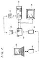
- FIG. 1 is a schematic block diagram showing the constitution of one embodiment of a camcorder to which a recording and reproducing apparatus of the present invention is applied. It is noted that an abbreviation of VTR (Video_Tape_Recorder) will be used to describe the function of a video tape recorder provided in an device.
- VTR Video_Tape_Recorder
- analog picture signals from an image pickup section 1 and from an analog input terminal 2 are supplied to an A/D (Analog_to_Digital) conversion circuit 3 and converted into digital picture signals by the circuit 3.
- the digital video signals converted by the A/D conversion circuit 3 and a digital picture signal from a digital input terminal 4 are supplied to a VTR section 6 through a change-over switch 5.
- the moving image video signals picked up by, for example, the image pickup section 1 or supplied to the analog input terminal 2 and the digital input terminal 4 are recorded on a magnetic recording medium (tape cassette which is not shown in FIG. 1) installed into the VTR section 6.
- the digital video signals from the A/D conversion circuit 3 and from the digital input terminal 4 are supplied to a semiconductor memory 7.
- This semiconductor memory 7 is controlled by a control signal from, for example, a memory control section 8, whereby still image signals each corresponding to an arbitrary one frame in the picture signals picked up by, for example, the image pickup section 1 or the picture signal supplied to the analog input terminal 2 or the digital input terminal 4 are digitally recorded on the semiconductor memory 7. It is noted that the semiconductor memory 7 is nonvolatile and detachable from an device.
- the semiconductor memory 7 is controlled by the control signal from, for example, the memory control section 8, still image signals recorded in, for example, the semiconductor memory 7 and each corresponding to one frame are repeatedly reproduced.
- a reproduction signal from the semiconductor memory 7 is supplied to a rate conversion circuit 9.
- the rate conversion circuit 9 detects the data rate of the reproduction signal based on an ID signal on the header portion of the signal. If the data rate, in the representation of a ratio of luminance signal (Y) : first color signal (R - Y) : second luminance signal (B - Y), is 4 : 4 : 4, then it is converted into 4 : 2 : 2 or 4 : 1 : 1.
- the detail of the rate conversion circuit 9 will be described later.
- the digital video signal having a converted data rate is supplied from the rate conversion circuit 9 to the VTR section 6 through the change-over switch 5.
- a video signal in which the still image signals recorded in, for example, the semiconductor memory 7 and each corresponding to one frame are repeatedly reproduced is recorded on the magnetic recording medium installed into the VTR section 6.
- the digital video signals repeatedly reproduced from the semiconductor memory 7 and having a data rate converted by the data conversion circuit 9 and the digital video signals reproduced from the VTR section 6 are selectively fetched at a switch 10.
- the digital video signals fetched at the switch 10 are supplied to a D/A (Digital_to_Analog) conversion circuit 11 and, at the same time, fetched at a digital output terminal 12.
- the analog video signals converted by the D/A conversion circuit 11 are supplied to a display section 13 consisting of a liquid crystal display unit or the like and built in the device and, at the same time, fetched at an analog output terminal 14.
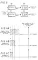
- a video signal of moving images picked up by or supplied to a camcorder device 100 is recorded on a tape cassette as shown in, for example, FIG. 2.
- the tape cassette 101 is then taken out and installed into a video tape deck 103, whereby the moving image video signal recorded on the tape cassette 101 is reproduced and displayed on, for example, an image receiver 104.
- the moving image picture signal from the camcorder device 100 may be directly supplied to the video tape deck 103 or to the image receiver 104.
- arbitrary frames of the moving image video signal picked up by or supplied to the device 100 are recorded one by one as still image signals by a semiconductor memory 102.
- the semiconductor memory 102 is then taken out and installed into a personal computer 105, whereby the still image signals recorded on the semiconductor memory 102 are captured into the computer 105 and displayed on, for example, a monitor. In that case, it is not necessary to separately prepare a video signal capture circuit or the like.
- the still image signals can be captured by using the installation section or the like of the general purpose semiconductor memory 102.
- the still image signals generated by, for example, the personal computer 105 can be recorded on the semiconductor memory 102 and supplied to the device 100.
- the data rate of the still image signals recorded on the semiconductor memory 102 from the personal computer 105 is 4 : 2 : 2 or 4 : 1 : 1
- the still image signals can be processed in the device 100 as they are.
- the data rate of the still image signals recorded on the semiconductor memory 102 is 4 : 4 : 4
- the rate is converted into 4 : 2 : 2 or 4 : 1 : 1 by the above-stated rate conversion circuit 9 and the still image signals are processed thereafter in the device 100.
- a signal supplied at a data rate of 4 : 4 : 4 is supplied to a pre-filter 201 for converting a signal into a signal at a data rate of 4 : 2 : 2 and to a pre-filter 202 for converting a signal into a signal at a data rate of 4 : 1 : 1.
- Signals from the pre-filters 201 and 202 are supplied to a thinning-out circuit 203 for converting a data rate from 4 : 4 : 4 into 4 : 2 : 2 and a thinning-out circuit 204 for converting a data rate from 4 : 4 : 4 into 4 : 1 : 1, respectively.
- the data rate of the supplied signal is converted from, for example, 4 : 4 : 4 into 4 : 2 : 2 or 4 : 1 : 1 and then the signal is subjected to processing.
- the pass bands of the pre-filters 201 and 202 are set as shown in, for example, FIG. 4. That is to say, if the sampling rate of a color signal at a data rate of, for example, 4 : 4 : 4 is that indicated by a right arrow in FIG. 4, the color signal at a data rate of 4 : 4 : 4 has a band shown in FIG. 4A.
- the pass band of the pre-filter 201 is limited to 1/2 of that of an original signal as shown in FIG. 4B.
- the pass band of the pre-filter 202 is limited to 1/4 of that of the original signal as shown in FIG. 4C.
- the sampling frequency of the color signal at a data rate of 4 : 2 : 2 is 1/2 of that of the original color signal at a data rate of 4 : 4 : 4. Due to this, the band of the color signal is limited to 1/4 of the original sampling frequency, thereby making it possible to eliminate trouble such as loop-back distortion. Likewise, the band of a color signal at a data rate of 4 : 1 : 1 is limited to 1/8 of the original sampling frequency, thereby making it possible to eliminate trouble such as loop-back distortion.
- FIG. 5 shows the concrete constitution of the pre-filters 201 and 202.
- each of the pre-filters 201 and 202 is constituted by a digital filter for arbitrarily weighting a plurality of taps at every unit delay time.
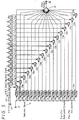
- a color signal at a data rate of 4 : 4 : 4 supplied to, for example, an input terminal 20 is supplied to 16 data latch circuits 21a to 21p connected in series.
- Clock signals at the sampling rate of the color signal having a data rate of 4 : 4 : 4 are supplied from a terminal 22 to the clock terminals of the data latch circuits 21a to 21p, respectively.
- the data latch circuits 21a to 21p hold the respective sampling values of the color signal at a data rate of 4 : 4 : 4. Then, 17 taps are led out from the inputs/outputs of the data latch circuits 21a to 21p and signals obtained at these taps are supplied to multipliers 23a to 23q for weighting, respectively. Further, tap coefficients from ROM's ( Read_only_Memories) 24a to 24q are supplied to the multipliers 23a to 23q, respectively. Signals weighted with the tap coefficients are added together by an adder 25 and fetched at an output terminal 26.
- tap coefficients for constituting a low-pass filter having a frequency of 1/4 or 1/8 of the original sampling frequency stated above used as a cut-off frequency are fetched from the ROM'S 24a to 24q and supplied to the multipliers 23a to 23q, respectively.
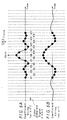
- tap frequencies as shown in FIG. 6 are employed.
- a curve of an SINC function ( SinX/X ) which is an ideal low-pass filter, is sampled equidistantly and symmetrically about a vertical axis and obtained sample values are used as the respective tap coefficients.
- a color signal at a data rate of 4 : 4 : 4 is converted into a signal at a data rate of 4 : 2 : 2
- sample values at sampling intervals as shown in, for example, FIG. 6A are used as tap coefficients.
- a color signal at a data rate of 4 : 4 : 4 is converted into a signal at a data rate of 4 : 1 : 1
- sample values obtained by conducting sampling at a density twice as large as that used to convert the data rate into 4 : 2 : 2 are used as tap coefficients as shown in FIG. 6B.
- the infinite taps are actually required, the infinite taps are unpractical to realize a low-pass filter. In this embodiment, therefore, the number of taps is limited to, for example, 17 to realize a low-pass filter.
- gain setting is made so that the sum of tap coefficients is 1. Consequently, a low-pass filter with frequency corresponding to 1/4 or 1/8 of the original sampling frequency stated above used as cut-off frequency can be constituted.
- the above-stated pre-filters 201 and 202 can be realized with the same circuit arrangement only by changing over tap coefficients.
- tap coefficients for both filters 201 and 202 are stored in the ROM's 24a to 24q and changed over by a change-over signal from, for example, a terminal 27, whereby the pre-filters 201 and 202 can be realized with the same circuit arrangement.
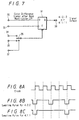
- FIG. 7 shows the concrete constitution of the thinning-out circuits 203 and 202.
- Each of the thinning-out circuits is constituted by a flip-flop 31 with an enable terminal.
- the color signal having a limited band is supplied from the pre-filters 201 or 202 to the data terminal D of the flip-flop 31, and a clock signal for a data rate of 4 : 4 : 4 is supplied to a clock terminal 33.
- the clock signal may be, for example, a signal shown in FIG. 8A.
- Sampling pulses both for a date rate of 4 : 2 : 2 and for a data rate of 4 : 1 : 1 as shown in FIGS. 8B and 8C, respectively, are supplied to terminals 34 and 35.
- the sampling pulses from these terminals 34 and 35 are supplied to a change-over switch 36.
- the change-over switch 36 is selected by a change-over signal for changing over the data rate of the output signal from a change-over terminal 37 to 4 : 2 : 2 and 4 : 1 : 1.
- the selected sampling pulse is supplied to the enable terminal E of the flip-flop 31.
- the flip-flop 31 then fetches a signal only at the timing of each sampling pulse and thins out the signal.
- the thinned-out signal is fetched at an output terminal 38.
- a color signal at a data rate of, for example, 4 : 4 : 4 is thinned out so as to change the data rate to 4 : 2 : 2
- the band of the color signal is first limited to 1/4 of the original sampling frequency and then the color signal is thinned out so as to change the data rate to 4 : 2 : 2.
- the band of the color signal is first limited to 1/8 of the original sampling frequency and then the color signal is thinned out so as to change the data rate to 4 : 1 : 1. It is, thus, possible to convert data rate without trouble such as loop-back distortion.
- the data rate an sampling frequency of an original signal is provided as, for example, an ID signal on the header portion of the signal. Due to this, the data rate and sampling frequency can be known by utilizing the ID signal. If a data rate desired by, for example, a user is set, whereby the data rate of the original signal is converted into a data rate desired by the user.
- the device is provided with conversion means for converting a signal at a data rate used for the transmission of, for example, still images into a signal at a data rate used for picture images, whereby a signal at a data rate used for the transmission of, for example, still images and formed in another arbitrary equipment can be converted into a signal at a data rate used for the transmission of, for example, moving images employed within the device, the converted signal can be displayed on, for example, a display unit built in the device and recorded as a continuous video signal on a videocassette or the like or outputted to an external unit.
- still image signals recorded at, for example, a different data rate and supplied from a semiconductor memory or the like cannot be fetched at the data rate of, for example, video signals.
- Still image signals processed by, for example, a personal computer and recorded on a semiconductor memory or the like cannot be displayed on a display unit built in, for example, a digital camcorder or recorded on a videocassette.
- the present invention can easily overcome these conventional disadvantages.
- converted data rates employed in the above-stated apparatus should not be limited to the above combination.
- contents of converted signals should not be limited to those of still image signals and moving image video signals as stated above.
- conversion means supplied with signals at the first and second data rates used for the transmission of moving images and a signal at the third data rate used for the transmission of still images, for converting the signal at the third data rate into a signal at the second data rate.
- the provision of this conversion means allows a signal at a data rate used for, for example, the transmission of still images formed by another arbitrary equipment to be converted into a signal at a data rate used for the transmission of, for example, moving images, to be displayed on, for example, a display unit built in the apparatus and to be recorded on a videocassette or the like as a continuous video signal or to be outputted to an external unit.
- conversion means for converting a signal at a data rate, for example, used for the transmission of still images into a signal at a data rate used for the transmission of moving images.
- the provision of the conversion means allows a signal at the data rate, for example, used for the transmission of still images formed by another arbitrary equipment to be converted into a signal at a data rate, for example, used for the transmission of moving images used in a device, to display the converted signal on, for example, a display unit built in the device, to record the signal as a continuous video signal on a videocassette or the like or to output the signal to an external unit.
- the conversion means has a pre-filter corresponding to the first and second data rates, and thinning-out means for converting the third data rate into the first and second data rates, respectively, whereby it is possible to conduct good data conversion without trouble such as loop-back distortion.
- the pre-filter is a digital filter for arbitrarily weighting a plurality of taps according to unit delay time, and has switching means for changing over tap coefficients according to the first data rate, whereby it is possible to conduct good data rate conversion with a simple constitution.
- the first data rate has a ratio of luminance signal : first color signal : second color signal of 4 : 2 : 2
- the second data rate has a ratio of luminance signal : first color signal : second color signal of 4 : 1 : 1
- the third data rate has a ratio of luminance signal : first color signal : second color signal of 4 : 4 : 4.
- still image signals recorded at, for example, a different data rate and supplied from a semiconductor memory or the like cannot be fetched at the data rate of, for example, video signals.
- Still image signals processed by, for example, a personal computer and recorded on a semiconductor memory or the like cannot be displayed on a display unit built in, for example, a digital camcorder or recorded on a videocassette.
- Embodiments of the present invention can easily overcome these conventional disadvantages.
Landscapes
- Engineering & Computer Science (AREA)
- Multimedia (AREA)
- Signal Processing (AREA)
- Computer Graphics (AREA)
- Television Signal Processing For Recording (AREA)
- Signal Processing For Digital Recording And Reproducing (AREA)
Applications Claiming Priority (2)
| Application Number | Priority Date | Filing Date | Title |
|---|---|---|---|
| JP20365899 | 1999-07-16 | ||
| JP11203658A JP2001036850A (ja) | 1999-07-16 | 1999-07-16 | 記録装置、記録再生装置、記録方法、記録再生方法、及び撮像装置 |
Publications (3)
| Publication Number | Publication Date |
|---|---|
| EP1069781A2 true EP1069781A2 (de) | 2001-01-17 |
| EP1069781A3 EP1069781A3 (de) | 2003-12-17 |
| EP1069781B1 EP1069781B1 (de) | 2011-05-25 |
Family
ID=16477715
Family Applications (1)
| Application Number | Title | Priority Date | Filing Date |
|---|---|---|---|
| EP00305879A Expired - Lifetime EP1069781B1 (de) | 1999-07-16 | 2000-07-12 | Videosignal-Aufnahme- und/oder -Wiedergabeanlage und -Verfahren, und Bildaufnahmeanlage |
Country Status (8)
| Country | Link |
|---|---|
| US (1) | US6785462B1 (de) |
| EP (1) | EP1069781B1 (de) |
| JP (1) | JP2001036850A (de) |
| KR (1) | KR100761228B1 (de) |
| CN (1) | CN1148745C (de) |
| CA (1) | CA2313998C (de) |
| MY (1) | MY125432A (de) |
| SG (1) | SG92719A1 (de) |
Families Citing this family (3)
| Publication number | Priority date | Publication date | Assignee | Title |
|---|---|---|---|---|
| US7496283B2 (en) | 2002-06-28 | 2009-02-24 | Microsoft Corporation | Methods and systems for processing digital data rate and directional playback changes |
| EP1511004A3 (de) * | 2003-08-19 | 2010-01-27 | Sony Corporation | Speichersteuerung, Speichersteuerungsverfahren, Frequenzumwandlungsvorrichtung, Frequenzumwandlunsverfahren, Bildsignalverarbeitungsvorrichtung, Bildsignalverarbeitungsverfahren und Programm zur Ausführung dieser Verfahren |
| JP4794911B2 (ja) * | 2005-05-31 | 2011-10-19 | キヤノン株式会社 | 画像処理装置 |
Citations (3)
| Publication number | Priority date | Publication date | Assignee | Title |
|---|---|---|---|---|
| JPH0970044A (ja) | 1995-08-31 | 1997-03-11 | Sony Corp | 画像信号処理装置および方法 |
| EP0844794A2 (de) | 1996-11-22 | 1998-05-27 | Victor Company of Japan, Ltd. | Vorrichtung zur Aufnahme digitaler Videosignalen und Vorrichtung zur Wiedergabe digitaler Videosignalen |
| WO1998044729A1 (fr) | 1997-04-03 | 1998-10-08 | Sony Corporation | Dispositif et procede d'enregistrement/reproduction |
Family Cites Families (9)
| Publication number | Priority date | Publication date | Assignee | Title |
|---|---|---|---|---|
| GB1412091A (en) * | 1973-01-17 | 1975-10-29 | Sony Corp | Systems for recording and reproducing colour television signals |
| JPS583384A (ja) * | 1981-06-29 | 1983-01-10 | Fuji Photo Film Co Ltd | スチル/ム−ビ−兼用電子カメラ |
| US4651227A (en) * | 1982-08-20 | 1987-03-17 | Olympus Optical Co., Ltd. | Video signal recording apparatus with A/D conversion |
| JP2995847B2 (ja) * | 1990-10-23 | 1999-12-27 | ソニー株式会社 | 記録再生装置 |
| JP3104085B2 (ja) * | 1991-10-18 | 2000-10-30 | ソニー株式会社 | 記録再生装置用送出システム |
| CA2081742C (en) * | 1991-11-13 | 2000-05-23 | Anthony M. Radice | Apparatus and method for recording random data on a digital video recorder |
| JPH0779449A (ja) * | 1993-09-06 | 1995-03-20 | Sony Corp | Vtr装置 |
| JPH07236151A (ja) * | 1994-02-23 | 1995-09-05 | Sony Corp | デジタルビデオスイッチャ |
| KR100225326B1 (ko) * | 1994-09-26 | 1999-10-15 | 다니구찌 이찌로오, 기타오카 다카시 | 디지탈영상신호기록재생장치 및 그 기록재생방법 |
-
1999
- 1999-07-16 JP JP11203658A patent/JP2001036850A/ja active Pending
-
2000
- 2000-07-06 SG SG200003813A patent/SG92719A1/en unknown
- 2000-07-07 MY MYPI20003109 patent/MY125432A/en unknown
- 2000-07-12 EP EP00305879A patent/EP1069781B1/de not_active Expired - Lifetime
- 2000-07-13 CA CA002313998A patent/CA2313998C/en not_active Expired - Fee Related
- 2000-07-13 KR KR1020000040161A patent/KR100761228B1/ko not_active Expired - Fee Related
- 2000-07-14 US US09/616,713 patent/US6785462B1/en not_active Expired - Fee Related
- 2000-07-16 CN CNB001240307A patent/CN1148745C/zh not_active Expired - Fee Related
Patent Citations (5)
| Publication number | Priority date | Publication date | Assignee | Title |
|---|---|---|---|---|
| JPH0970044A (ja) | 1995-08-31 | 1997-03-11 | Sony Corp | 画像信号処理装置および方法 |
| US5930397A (en) | 1995-08-31 | 1999-07-27 | Sony Corporation | Apparatus and method for processing image signal |
| EP0844794A2 (de) | 1996-11-22 | 1998-05-27 | Victor Company of Japan, Ltd. | Vorrichtung zur Aufnahme digitaler Videosignalen und Vorrichtung zur Wiedergabe digitaler Videosignalen |
| WO1998044729A1 (fr) | 1997-04-03 | 1998-10-08 | Sony Corporation | Dispositif et procede d'enregistrement/reproduction |
| US6438316B1 (en) | 1997-04-03 | 2002-08-20 | Sony Corporation | Recording/reproducing apparatus and method for including line numbers |
Also Published As
| Publication number | Publication date |
|---|---|
| SG92719A1 (en) | 2002-11-19 |
| KR100761228B1 (ko) | 2007-09-28 |
| CA2313998C (en) | 2006-06-13 |
| CN1281223A (zh) | 2001-01-24 |
| EP1069781B1 (de) | 2011-05-25 |
| KR20010015321A (ko) | 2001-02-26 |
| CA2313998A1 (en) | 2001-01-16 |
| MY125432A (en) | 2006-07-31 |
| US6785462B1 (en) | 2004-08-31 |
| CN1148745C (zh) | 2004-05-05 |
| JP2001036850A (ja) | 2001-02-09 |
| EP1069781A3 (de) | 2003-12-17 |
Similar Documents
| Publication | Publication Date | Title |
|---|---|---|
| KR100666290B1 (ko) | 촬상 장치 및 촬상 방법 | |
| EP0868090B1 (de) | Digitale Videokamera und Aufzeichnungsvorrichtung | |
| EP0302500A2 (de) | Schaltung zur Verarbeitung eines Farbdifferenzsignals unter Verwendung der Änderung eines Luminanzsignals | |
| KR920010512B1 (ko) | 촬상장치 | |
| US5914755A (en) | Image transmission apparatus | |
| US6785462B1 (en) | Recording and reproducing apparatus | |
| EP0753961B1 (de) | Dieselbe Hardware für Aufnahme und Wiedergabe benutzende Bildverarbeitungsvorrichtung | |
| JP2000106642A (ja) | 撮像装置 | |
| JP2001086394A (ja) | 撮像装置 | |
| US5911028A (en) | Video signal and camera signal processing apparatus | |
| JP3254211B2 (ja) | 電子スチルカメラ | |
| KR100275903B1 (ko) | 정지화면을보면서동영상촬영기록이가능한디지털비디오캠코더 | |
| US4974079A (en) | Band compressed video signal transmission system | |
| JP3782510B2 (ja) | 画像処理装置 | |
| KR100195112B1 (ko) | 윈도우 기능을 갖는 디지털 캠코더 | |
| KR900002294Y1 (ko) | 영상기록 재생기의 정지화면 확대회로 | |
| JPH08265658A (ja) | 映像・音声出力回路 | |
| JPH05236508A (ja) | 撮像記録システム及び記録装置 | |
| KR20050090799A (ko) | 복합촬영장치 및 그것을 이용한 음향기록방법 | |
| JPH0837672A (ja) | カラーコンポーネントビデオ信号方式変換装置 | |
| JPH114409A (ja) | 画像記録装置 | |
| JPH0888799A (ja) | 映像出力装置及びそれを用いた画像処理システム | |
| JPH06339108A (ja) | 撮像装置 | |
| JPH04298166A (ja) | 画像揺れ補正装置付きテレビジョン受信機 | |
| JPH11168642A (ja) | 画像出力システム |
Legal Events
| Date | Code | Title | Description |
|---|---|---|---|
| PUAI | Public reference made under article 153(3) epc to a published international application that has entered the european phase |
Free format text: ORIGINAL CODE: 0009012 |
|
| AK | Designated contracting states |
Kind code of ref document: A2 Designated state(s): AT BE CH CY DE DK ES FI FR GB GR IE IT LI LU MC NL PT SE |
|
| AX | Request for extension of the european patent |
Free format text: AL;LT;LV;MK;RO;SI |
|
| PUAL | Search report despatched |
Free format text: ORIGINAL CODE: 0009013 |
|
| AK | Designated contracting states |
Kind code of ref document: A3 Designated state(s): AT BE CH CY DE DK ES FI FR GB GR IE IT LI LU MC NL PT SE |
|
| AX | Request for extension of the european patent |
Extension state: AL LT LV MK RO SI |
|
| 17P | Request for examination filed |
Effective date: 20040601 |
|
| AKX | Designation fees paid |
Designated state(s): DE FR GB |
|
| 17Q | First examination report despatched |
Effective date: 20060721 |
|
| GRAP | Despatch of communication of intention to grant a patent |
Free format text: ORIGINAL CODE: EPIDOSNIGR1 |
|
| GRAS | Grant fee paid |
Free format text: ORIGINAL CODE: EPIDOSNIGR3 |
|
| GRAA | (expected) grant |
Free format text: ORIGINAL CODE: 0009210 |
|
| AK | Designated contracting states |
Kind code of ref document: B1 Designated state(s): DE FR GB |
|
| REG | Reference to a national code |
Ref country code: GB Ref legal event code: FG4D |
|
| REG | Reference to a national code |
Ref country code: DE Ref legal event code: R096 Ref document number: 60046000 Country of ref document: DE Effective date: 20110707 |
|
| PLBE | No opposition filed within time limit |
Free format text: ORIGINAL CODE: 0009261 |
|
| STAA | Information on the status of an ep patent application or granted ep patent |
Free format text: STATUS: NO OPPOSITION FILED WITHIN TIME LIMIT |
|
| 26N | No opposition filed |
Effective date: 20120228 |
|
| REG | Reference to a national code |
Ref country code: DE Ref legal event code: R097 Ref document number: 60046000 Country of ref document: DE Effective date: 20120228 |
|
| REG | Reference to a national code |
Ref country code: GB Ref legal event code: 746 Effective date: 20120703 |
|
| REG | Reference to a national code |
Ref country code: DE Ref legal event code: R084 Ref document number: 60046000 Country of ref document: DE Effective date: 20120614 |
|
| PGFP | Annual fee paid to national office [announced via postgrant information from national office to epo] |
Ref country code: GB Payment date: 20120719 Year of fee payment: 13 |
|
| PGFP | Annual fee paid to national office [announced via postgrant information from national office to epo] |
Ref country code: FR Payment date: 20120806 Year of fee payment: 13 Ref country code: DE Payment date: 20120822 Year of fee payment: 13 |
|
| GBPC | Gb: european patent ceased through non-payment of renewal fee |
Effective date: 20130712 |
|
| REG | Reference to a national code |
Ref country code: FR Ref legal event code: ST Effective date: 20140331 |
|
| PG25 | Lapsed in a contracting state [announced via postgrant information from national office to epo] |
Ref country code: DE Free format text: LAPSE BECAUSE OF NON-PAYMENT OF DUE FEES Effective date: 20140201 Ref country code: GB Free format text: LAPSE BECAUSE OF NON-PAYMENT OF DUE FEES Effective date: 20130712 |
|
| REG | Reference to a national code |
Ref country code: DE Ref legal event code: R119 Ref document number: 60046000 Country of ref document: DE Effective date: 20140201 |
|
| PG25 | Lapsed in a contracting state [announced via postgrant information from national office to epo] |
Ref country code: FR Free format text: LAPSE BECAUSE OF NON-PAYMENT OF DUE FEES Effective date: 20130731 |