EP1069674B1 - Schaltnetzteil - Google Patents
Schaltnetzteil Download PDFInfo
- Publication number
- EP1069674B1 EP1069674B1 EP00114508A EP00114508A EP1069674B1 EP 1069674 B1 EP1069674 B1 EP 1069674B1 EP 00114508 A EP00114508 A EP 00114508A EP 00114508 A EP00114508 A EP 00114508A EP 1069674 B1 EP1069674 B1 EP 1069674B1
- Authority
- EP
- European Patent Office
- Prior art keywords
- power supply
- switched
- mode power
- switch
- coupling element
- Prior art date
- Legal status (The legal status is an assumption and is not a legal conclusion. Google has not performed a legal analysis and makes no representation as to the accuracy of the status listed.)
- Expired - Lifetime
Links
Images
Classifications
-
- H—ELECTRICITY
- H02—GENERATION; CONVERSION OR DISTRIBUTION OF ELECTRIC POWER
- H02M—APPARATUS FOR CONVERSION BETWEEN AC AND AC, BETWEEN AC AND DC, OR BETWEEN DC AND DC, AND FOR USE WITH MAINS OR SIMILAR POWER SUPPLY SYSTEMS; CONVERSION OF DC OR AC INPUT POWER INTO SURGE OUTPUT POWER; CONTROL OR REGULATION THEREOF
- H02M3/00—Conversion of DC power input into DC power output
- H02M3/22—Conversion of DC power input into DC power output with intermediate conversion into AC
- H02M3/24—Conversion of DC power input into DC power output with intermediate conversion into AC by static converters
- H02M3/28—Conversion of DC power input into DC power output with intermediate conversion into AC by static converters using discharge tubes with control electrode or semiconductor devices with control electrode to produce the intermediate AC
- H02M3/325—Conversion of DC power input into DC power output with intermediate conversion into AC by static converters using discharge tubes with control electrode or semiconductor devices with control electrode to produce the intermediate AC using devices of a triode or a transistor type requiring continuous application of a control signal
- H02M3/335—Conversion of DC power input into DC power output with intermediate conversion into AC by static converters using discharge tubes with control electrode or semiconductor devices with control electrode to produce the intermediate AC using devices of a triode or a transistor type requiring continuous application of a control signal using semiconductor devices only
- H02M3/338—Conversion of DC power input into DC power output with intermediate conversion into AC by static converters using discharge tubes with control electrode or semiconductor devices with control electrode to produce the intermediate AC using devices of a triode or a transistor type requiring continuous application of a control signal using semiconductor devices only in a self-oscillating arrangement
- H02M3/3385—Conversion of DC power input into DC power output with intermediate conversion into AC by static converters using discharge tubes with control electrode or semiconductor devices with control electrode to produce the intermediate AC using devices of a triode or a transistor type requiring continuous application of a control signal using semiconductor devices only in a self-oscillating arrangement with automatic control of output voltage or current
-
- H—ELECTRICITY
- H02—GENERATION; CONVERSION OR DISTRIBUTION OF ELECTRIC POWER
- H02M—APPARATUS FOR CONVERSION BETWEEN AC AND AC, BETWEEN AC AND DC, OR BETWEEN DC AND DC, AND FOR USE WITH MAINS OR SIMILAR POWER SUPPLY SYSTEMS; CONVERSION OF DC OR AC INPUT POWER INTO SURGE OUTPUT POWER; CONTROL OR REGULATION THEREOF
- H02M3/00—Conversion of DC power input into DC power output
- H02M3/22—Conversion of DC power input into DC power output with intermediate conversion into AC
- H02M3/24—Conversion of DC power input into DC power output with intermediate conversion into AC by static converters
- H02M3/28—Conversion of DC power input into DC power output with intermediate conversion into AC by static converters using discharge tubes with control electrode or semiconductor devices with control electrode to produce the intermediate AC
- H02M3/325—Conversion of DC power input into DC power output with intermediate conversion into AC by static converters using discharge tubes with control electrode or semiconductor devices with control electrode to produce the intermediate AC using devices of a triode or a transistor type requiring continuous application of a control signal
- H02M3/335—Conversion of DC power input into DC power output with intermediate conversion into AC by static converters using discharge tubes with control electrode or semiconductor devices with control electrode to produce the intermediate AC using devices of a triode or a transistor type requiring continuous application of a control signal using semiconductor devices only
- H02M3/33507—Conversion of DC power input into DC power output with intermediate conversion into AC by static converters using discharge tubes with control electrode or semiconductor devices with control electrode to produce the intermediate AC using devices of a triode or a transistor type requiring continuous application of a control signal using semiconductor devices only with automatic control of the output voltage or current, e.g. flyback converters
- H02M3/33523—Conversion of DC power input into DC power output with intermediate conversion into AC by static converters using discharge tubes with control electrode or semiconductor devices with control electrode to produce the intermediate AC using devices of a triode or a transistor type requiring continuous application of a control signal using semiconductor devices only with automatic control of the output voltage or current, e.g. flyback converters with galvanic isolation between input and output of both the power stage and the feedback loop
Definitions
- the present invention relates to a switched-mode power supply having a transformer, a switching transistor connected in series with a primary winding of the transformer, a control circuit and a secondary-side regulating stage.
- Switched-mode power supplies of this type are used in appliances for consumer electronics, for example.
- the two switched-mode power supplies are coupled to one another such that the larger switched-mode power supply is regulated by means of the small switched-mode power supply during normal operation, and the small switched-mode power supply oscillates using a dedicated oscillator in standby operation.
- the invention is based on the object of specifying a switched-mode power supply of the type mentioned in the introduction which has a very low power consumption.
- the switched-mode power supply of the invention has a transformer, a switching transistor connected in series with a primary winding of the transformer, a primary-side control circuit and a secondary-side regulating stage.
- the control circuit is used to drive the switching transistor.
- the secondary-side regulating circuit is used to drive a coupling element, which is used to transmit a regulating signal from the secondary to the primary.
- a first switch is situated between the control input of the switching transistor and a primary-side operating voltage
- a second switch is situated between the regulating stage and a secondary-side operating voltage, with the two operating voltages being able to be disconnected by means of the two switches using a single control signal.
- the isolating element transmits both the regulating information for the primary-side control circuit and the turn-off signal for the first switch.
- the control signal for turning off the two switches is applied to a control input of the second switch, and, when this switch is off, the secondary-side regulating stage is disconnected at the same time and the first switch is turned off via the coupling element.
- the coupling element is preferably an optocoupler driven on the secondary side by a transistor stage of the secondary-side regulating stage, at which both the switched-mode power supply's output voltage which is to be regulated and, via the second switch, the control signal information are present.
- the regulating stage and the optocoupler become completely non-live and consume no further power.
- the optocoupler is off on the primary side, which means that the first switch is also turned off, so that both the switching transistor and the control circuit become non-live.
- the switched-mode power supply is completely non-live except for the starting circuit, so that the power consumption is below 0.2 W in this state.
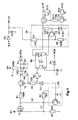
- the figure shows, on the primary side, a switching transistor T1 in series with a primary winding W1 of a transformer.
- the transformer is not shown in the figure; as is usual with appliances in entertainment electronics, it is designed with power supply isolation and, apart from the primary winding W1, contains one or more primary windings for operation of the switched-mode power supply, and, on the secondary, one or more windings for providing the required output voltages.
- the transistor T1 is a MOSFET controlled by a control circuit DR.
- the primary-side auxiliary winding W2a is used to provide an operating voltage VCC which is rectified via a diode D2 and is buffered by a capacitor C1.
- a starting circuit A which establishes a connection to the power supply rectifier or to a DC voltage produced from the power supply via a high-value resistor chain in a manner which is known, is used to provide the current necessary for starting the switched-mode power supply.
- Connected in parallel with the capacitor C1 is a zener diode D3, which limits the operating voltage VCC.
- the figure shows a winding W3 which, via a diode D5 and a capacitor C3, produces an output voltage UA which is to be stabilized.
- This output voltage UA is tapped off across a resistor R7 by a secondary-side regulating stage SR and is conditioned for transmission to the primary side. Transmission is effected by a coupling element, which is an optocoupler OK in this illustrative embodiment. Other coupling elements, such as transformers, can likewise be used.
- the regulating signal transmitted by the regulating stage SR via the optocoupler OK is applied to the control circuit DR, which converts this signal into a pulse-width-modulated control voltage U2 for driving the switching transistor T1.
- the control circuit DR also uses another voltage U1 for driving, said voltage being applied across a resistor R3 and being an indication of the current flowing through the switching transistor T1.
- the switched-mode power supply can be designed both as a free-running switched-mode power supply which changes its switching frequency depending on the load, and as a switched-mode power supply operating with pulse-width modulation at a fixed switching frequency.
- a switched-mode power supply of this type is specified in EP 0 808 015 A2, for example. In this case, the regulation is frequently applied to a secondary-side output voltage, since this allows better stabilization of the output voltage.
- a resistor R1 in order to allow the control voltage U2 to be decoupled from the control circuit DR and the operating voltage VCC.
- a first switch T2 in this illustrative embodiment a transistor, which can turn off the operating voltage VCC.
- the control input of this switch is connected via resistors R5 and R6 to the optocoupler OK, which can be used to drive the switch T2 from the secondary side.
- the optocoupler OK has a high impedance on the primary side, then the operating voltage VCC is applied to the control input of the first switch T2 via a resistor R4, so that no current can flow via the emitter-base junction of the transistor T2, which means that the latter is off. If a low voltage is applied to the control input of the switch T2, then the latter turns on.
- the control circuit DR is likewise connected to the optocoupler OK via a diode D1 and the resistor R6, so that said optocoupler transmits both the secondary-side regulating information and the turn-off signal for the first switch T2.
- the optocoupler contains a light-emitting diode operated via connections 3 and 4.
- This diode is driven by a transistor stage having a transistor T3 controlling the current through the light-emitting diode in the optocoupler, a secondary-side operating voltage UB being applied to the connection 3 of the optocoupler via a second switch T4.
- the control input of the transistor T3 has a constant voltage applied to it which is formed by a voltage divider which contains a resistor R9 and a zener diode D6 and which has the operating voltage UB across it during operation.
- the emitter of the transistor T3 is at the output voltage UA to be regulated, so that the current through the light-emitting diode of the optocoupler OK is controlled via the base-emitter junction of the transistor T3 as a function of the output voltage UA.
- a variable zener diode can also be used for transmitting the regulating signal.
- the second switch T4 is turned on and off via a transistor stage T5 having resistors R11, R12 by a control signal US from a digital circuit. If the control signal US is "zero", then transistor T5 is off, which means that the transistor T4 is also off, because its control input is in this case at a high potential via the resistor R10.
- the switch T4 is off, then neither the transistor stage having the transistor T3 nor the light-emitting diode in the optocoupler OK are live. This means that the photoresistance of the optocoupler OK is also high, so that the first switch T2 is likewise off, as described above. In this case, the control circuit DR also switches off, since no more current flows through the diode D1.
- the regulating transmission via the optocoupler OK is carried out so that, when the output voltage UA is too high, the output of the optocoupler OK, connections 1 and 2, has a relatively high impedance, and, when the output voltage UA is too low, it has a relatively low impedance.
- the MOSFET used as a switching transistor is off at a control voltage U2 of below approximately 2 volts.
- the control circuit DR is likewise decoupled from the operating voltage VCC by the diode D1. If the control signal US is zero, therefore, then neither the secondary-side switching stages having the transistors T3, T4 and T5 nor the transistors T1 and T2 and the primary-side control circuit DR are live. When the switched-mode power supply is in the turned-off state, this means that only the starting circuit A consumes a very small amount of power.
- connection 2 of the optocoupler OK is connected to a flyback negative winding W2b via a diode D4, so that the switched-mode power supply starts softly when it is turned on.
- the negative voltage present on the winding W2b during the turned-off phase of the switching transistor T1 is still relatively low, so that the regulating signal transmitted via the optocoupler OK is attenuated.
- the flyback negative voltage has developed on the winding W2b and the capacitor C2 is charged to a corresponding negative voltage, does the regulating signal become active at full strength for the control circuit DR.
- a switched-mode power supply of this type can be used, in particular, in appliances for consumer electronics, and allows the power consumption to be kept very low in standby operation.
- flyback converters are predominantly used as the power supply unit, but the invention can also be used for other types of switched-mode power supplies.
- the second operating voltage UB must always be present in order to turn on the switched-mode power supply. This operating voltage can be provided by a second power supply unit, for example, or by a battery or a rechargeable battery.
Landscapes
- Engineering & Computer Science (AREA)
- Power Engineering (AREA)
- Dc-Dc Converters (AREA)
Claims (10)
- Schaltnetzteil mit einem Transformator, einem Schalttransistor (T1) in Serie zu einer Primärwicklung (W1) des Transformators, einer primärseitigen Kontrollschaltung (DR) und mit einer sekundärseitigen Regelstufe (SR), wobei ein Steuereingang des Schalttransistors (T1) mit einem ersten Schalter (T2) verbunden ist, dadurch gekennzeichnet, daß ein zweiter Schalter (T4) zwischen der Regelstufe (SR) und einer Betriebsspannung (UB) liegt, und daß das Sperren des zweiten Schalters (T4) gleichzeitig das Sperren des ersten Schalters (T2) bewirkt.
- Schaltnetzteil nach Anspruch 1, dadurch gekennzeichnet, daß die Regelstufe (SR) über ein Koppelelement (OK) sowohl mit der Kontrollschaltung (DR) als auch mit dem ersten Schalter (T2) verbunden ist.
- Schaltnetzteil nach Anspruch 1 oder 2, dadurch gekennzeichnet, daß die Regelstufe (SR) eine Transistorstufe (T3, R8, R9, D6) aufweist, deren Anschlüsse mit einer Ausgangsspannung des Schaltnetzteiles (UA), dem Koppelelement (OK) und dem zweiten Schalter (T4) in Verbindung stehen sowohl zur Übertragung eines Regelsignales als auch eines Steuersignales (US).
- Schaltnetzteil nach Anspruch 2 oder 3, dadurch gekennzeichnet, daß mittels eines Steuersignals (US) der zweite Schalter (T4) sperrbar ist, so daß die Versorgungsspannung (UB) für die Regelstufe (SR) abgeschaltet wird und hierdurch über das Koppelelement (OK) der erste Schalter (T2) gesperrt wird.
- Schaltnetzteil nach einem der vorangehenden Ansprüche, dadurch gekennzeichnet, daß der erste Schalter (T2) zwischen dem Steuereingang des Schalttransistors (T1) und einer primärseitigen Betriebsspannung (VCC) liegt.
- Schaltnetzteil nach einem der vorangehenden Ansprüche, dadurch gekennzeichnet, daß das Koppelelement (OK) primärseitig mit einem Anschluß (2) mit einer Hilfswicklung (W2b) des Transformators und mit einem anderen Anschluß (1) sowohl mit dem ersten Schalter (T2) als auch mit der Kontrollschaltung (DR) in Verbindung steht.
- Schaltnetzteil nach Anspruch 6, dadurch gekennzeichnet, daß zwischen der Kontrollschaltung (DR) und dem Koppelelement (OK) sowie dem ersten Schalter (T2) eine Diode (D1) angeordnet ist.
- Schaltnetzteil nach Anspruch 5, 6 oder 7, dadurch gekennzeichnet, daß der Steuereingang des ersten Schalters (T2) über einen Widerstand (R4) mit der primärseitigen Betriebsspannung (VCC) verbunden ist, über den an diesem Steuereingang eine hohe Spannung anliegt zum Sperren des Schalters (T2), wenn das Koppelelement (OK) hochohmig ist.
- Schaltnetzteil nach einem der vorangehenden Ansprüche 2 - 8, dadurch gekennzeichnet, daß das Koppelelement (OK) ein Optokoppler ist, der primärseitig mit einem EmitterAnschluß (2) an einer Flyback-Negativ-Wicklung (W2b) anliegt, so daß beim Einschalten des Schaltnetzteiles ein Softstart durchgeführt wird.
- Schaltnetzteil nach einem der vorangehenden Ansprüche, dadurch gekennzeichnet, daß die sekundärseitige Betriebsspannung (UB) von einem anderen Netzteil erzeugt wird, und daß das Schaltnetzteil als zusätzliches Netzteil dient, das über das Steuersignal (US) vollständig abschaltbar als auch wieder einschaltbar ist.
Applications Claiming Priority (2)
| Application Number | Priority Date | Filing Date | Title |
|---|---|---|---|
| DE19932711A DE19932711A1 (de) | 1999-07-16 | 1999-07-16 | Schaltnetzteil |
| DE19932711 | 1999-07-16 |
Publications (3)
| Publication Number | Publication Date |
|---|---|
| EP1069674A2 EP1069674A2 (de) | 2001-01-17 |
| EP1069674A3 EP1069674A3 (de) | 2001-12-19 |
| EP1069674B1 true EP1069674B1 (de) | 2003-06-11 |
Family
ID=7914616
Family Applications (1)
| Application Number | Title | Priority Date | Filing Date |
|---|---|---|---|
| EP00114508A Expired - Lifetime EP1069674B1 (de) | 1999-07-16 | 2000-07-06 | Schaltnetzteil |
Country Status (6)
| Country | Link |
|---|---|
| US (1) | US6349045B1 (de) |
| EP (1) | EP1069674B1 (de) |
| JP (1) | JP4488132B2 (de) |
| CN (1) | CN1144343C (de) |
| DE (2) | DE19932711A1 (de) |
| ES (1) | ES2200761T3 (de) |
Families Citing this family (8)
| Publication number | Priority date | Publication date | Assignee | Title |
|---|---|---|---|---|
| US7259971B1 (en) | 2003-08-04 | 2007-08-21 | Z-Axis, Inc. | Encapsulated electronic power converter with embedded AC components |
| US7319232B1 (en) * | 2005-06-06 | 2008-01-15 | National Semiconductor Corporation | Apparatus and method for high-bandwidth opto-coupler interface |
| WO2011051824A1 (en) * | 2009-10-30 | 2011-05-05 | Koninklijke Philips Electronics N.V. | Isolated power converter having reduced stanby power |
| FR2962268A1 (fr) * | 2010-07-05 | 2012-01-06 | Awox | Procede et dispositif pour diminuer la consommation d'appareils electriques |
| CN102664525B (zh) * | 2012-05-08 | 2014-08-27 | 成都芯源系统有限公司 | 一种开关电源电路 |
| US10098194B1 (en) * | 2016-09-06 | 2018-10-09 | Universal Lighting Technologies, Inc. | Current and voltage control circuit and method for a class II LED driver |
| US10362644B1 (en) | 2017-07-28 | 2019-07-23 | Universal Lighting Technologies, Inc. | Flyback converter with load condition control circuit |
| CN116865525A (zh) * | 2023-05-26 | 2023-10-10 | 上海新进芯微电子有限公司 | 开关电源的待机方法、开关电源、原边和副边控制电路 |
Family Cites Families (10)
| Publication number | Priority date | Publication date | Assignee | Title |
|---|---|---|---|---|
| DE3330039A1 (de) * | 1983-08-19 | 1985-02-28 | Siemens AG, 1000 Berlin und 8000 München | Sperrwandler-schaltnetzteil |
| DE3731645A1 (de) * | 1987-09-19 | 1989-03-30 | Thomson Brandt Gmbh | Schaltnetzteil |
| NL8900609A (nl) * | 1989-03-14 | 1990-10-01 | Nedap Nv | Stuurschakeling. |
| US5453921A (en) * | 1993-03-31 | 1995-09-26 | Thomson Consumer Electronics, Inc. | Feedback limited duty cycle switched mode power supply |
| JP2574261Y2 (ja) * | 1993-09-01 | 1998-06-11 | ヤマハ株式会社 | スイッチング電源回路 |
| ES2109565T3 (es) * | 1994-08-01 | 1998-01-16 | Siemens Ag | Convertidor de flujo con un circuito de salida adicional. |
| DE19545659A1 (de) * | 1995-12-07 | 1997-06-12 | Thomson Brandt Gmbh | Schaltnetzteil für Normalbetrieb und Bereitschaftsbetrieb |
| DE19600962A1 (de) * | 1996-01-12 | 1997-07-17 | Siemens Ag | Schaltnetzteil mit verlustleistungsarmem Standby-Betrieb |
| EP0803966B1 (de) * | 1996-04-23 | 2005-02-23 | Deutsche Thomson-Brandt Gmbh | Netzteil für ein Gerät mit Standby-Betrieb |
| US5995384A (en) * | 1997-07-31 | 1999-11-30 | Philips Electronics North America Corporation | Functional on/off switch for switched-mode power supply circuit with burst mode operation |
-
1999
- 1999-07-16 DE DE19932711A patent/DE19932711A1/de not_active Withdrawn
-
2000
- 2000-06-23 US US09/602,981 patent/US6349045B1/en not_active Expired - Lifetime
- 2000-07-06 ES ES00114508T patent/ES2200761T3/es not_active Expired - Lifetime
- 2000-07-06 DE DE60003265T patent/DE60003265T2/de not_active Expired - Lifetime
- 2000-07-06 EP EP00114508A patent/EP1069674B1/de not_active Expired - Lifetime
- 2000-07-13 CN CNB001202227A patent/CN1144343C/zh not_active Expired - Lifetime
- 2000-07-17 JP JP2000216403A patent/JP4488132B2/ja not_active Expired - Lifetime
Also Published As
| Publication number | Publication date |
|---|---|
| DE19932711A1 (de) | 2001-01-18 |
| CN1281287A (zh) | 2001-01-24 |
| ES2200761T3 (es) | 2004-03-16 |
| DE60003265D1 (de) | 2003-07-17 |
| JP4488132B2 (ja) | 2010-06-23 |
| US6349045B1 (en) | 2002-02-19 |
| DE60003265T2 (de) | 2003-12-11 |
| JP2001054282A (ja) | 2001-02-23 |
| EP1069674A3 (de) | 2001-12-19 |
| CN1144343C (zh) | 2004-03-31 |
| EP1069674A2 (de) | 2001-01-17 |
Similar Documents
| Publication | Publication Date | Title |
|---|---|---|
| EP0964503B1 (de) | Anordnung mit einem Schaltnetzteil und einem Mikroprozessor | |
| US5862044A (en) | Switching power supply unit | |
| CA1314932C (en) | Off-line switcher with battery reserve | |
| US6018467A (en) | Resonant mode power supply having an efficient low power stand-by mode | |
| EP1459431B1 (de) | Sperrleistungswandler | |
| JP2956681B2 (ja) | スイッチング電源の切換運転回路 | |
| KR100465577B1 (ko) | 보조 전원 장치용 고속 리셋 회로 | |
| US6385061B1 (en) | Switched mode power supply with programmable skipping mode | |
| JP3777239B2 (ja) | スイッチング電源部 | |
| EP1069674B1 (de) | Schaltnetzteil | |
| US8411476B2 (en) | Charge mode control | |
| US6031734A (en) | Switched-mode power supply with threshold value circuit | |
| US5973940A (en) | Switched-mode power supply for a load having a low power supply | |
| JP4072664B2 (ja) | 電子機器の電源装置 | |
| JP2004343708A (ja) | マイクロプロセッサと減磁回路と通常モード及び低電力モードを有するスイッチモード電源とを包含する装置及び表示ユニット | |
| WO2002015371B1 (en) | Switched magamp post regulator | |
| US6233164B1 (en) | Protection circuit for a switched-mode power supply | |
| US6208532B1 (en) | Switched-mode power supply that clock-pulse controls a switching element for supplying a rectified AC voltage to a primary winding of a transformer of the power supply | |
| JP7479313B2 (ja) | スイッチング電源装置 | |
| KR100333304B1 (ko) | 스위칭 전원회로의 웨이크업 회로 | |
| KR20080094565A (ko) | 정류기 회로를 포함하는 스위칭 모드 파워 서플라이 | |
| SE9601086L (sv) | Chopperströmkälla av flyback-typ | |
| CA2356187A1 (en) | A synchronous flyback converter | |
| JPH06133536A (ja) | 交直両用形電源装置 | |
| JP2000014132A (ja) | スイッチング電源 |
Legal Events
| Date | Code | Title | Description |
|---|---|---|---|
| PUAI | Public reference made under article 153(3) epc to a published international application that has entered the european phase |
Free format text: ORIGINAL CODE: 0009012 |
|
| AK | Designated contracting states |
Kind code of ref document: A2 Designated state(s): DE ES FR GB IT Kind code of ref document: A2 Designated state(s): AT BE CH CY DE DK ES FI FR GB GR IE IT LI LU MC NL PT SE |
|
| AX | Request for extension of the european patent |
Free format text: AL;LT;LV;MK;RO;SI |
|
| PUAL | Search report despatched |
Free format text: ORIGINAL CODE: 0009013 |
|
| AK | Designated contracting states |
Kind code of ref document: A3 Designated state(s): AT BE CH CY DE DK ES FI FR GB GR IE IT LI LU MC NL PT SE |
|
| AX | Request for extension of the european patent |
Free format text: AL;LT;LV;MK;RO;SI |
|
| 17P | Request for examination filed |
Effective date: 20020603 |
|
| AKX | Designation fees paid |
Free format text: DE ES FR GB IT |
|
| GRAH | Despatch of communication of intention to grant a patent |
Free format text: ORIGINAL CODE: EPIDOS IGRA |
|
| GRAH | Despatch of communication of intention to grant a patent |
Free format text: ORIGINAL CODE: EPIDOS IGRA |
|
| GRAA | (expected) grant |
Free format text: ORIGINAL CODE: 0009210 |
|
| AK | Designated contracting states |
Designated state(s): DE ES FR GB IT |
|
| REG | Reference to a national code |
Ref country code: GB Ref legal event code: FG4D |
|
| REG | Reference to a national code |
Ref country code: IE Ref legal event code: FG4D |
|
| REG | Reference to a national code |
Ref country code: GB Ref legal event code: 746 Effective date: 20030624 |
|
| REF | Corresponds to: |
Ref document number: 60003265 Country of ref document: DE Date of ref document: 20030717 Kind code of ref document: P |
|
| REG | Reference to a national code |
Ref country code: ES Ref legal event code: FG2A Ref document number: 2200761 Country of ref document: ES Kind code of ref document: T3 |
|
| ET | Fr: translation filed | ||
| PLBE | No opposition filed within time limit |
Free format text: ORIGINAL CODE: 0009261 |
|
| STAA | Information on the status of an ep patent application or granted ep patent |
Free format text: STATUS: NO OPPOSITION FILED WITHIN TIME LIMIT |
|
| REG | Reference to a national code |
Ref country code: FR Ref legal event code: D6 |
|
| REG | Reference to a national code |
Ref country code: IE Ref legal event code: MM4A |
|
| 26N | No opposition filed |
Effective date: 20040312 |
|
| REG | Reference to a national code |
Ref country code: FR Ref legal event code: PLFP Year of fee payment: 17 |
|
| REG | Reference to a national code |
Ref country code: FR Ref legal event code: PLFP Year of fee payment: 18 |
|
| REG | Reference to a national code |
Ref country code: FR Ref legal event code: PLFP Year of fee payment: 19 |
|
| REG | Reference to a national code |
Ref country code: GB Ref legal event code: 732E Free format text: REGISTERED BETWEEN 20180920 AND 20180926 |
|
| REG | Reference to a national code |
Ref country code: FR Ref legal event code: TP Owner name: THOMSON LICENSING DTV, FR Effective date: 20180913 |
|
| REG | Reference to a national code |
Ref country code: FR Ref legal event code: CA Effective date: 20180914 Ref country code: FR Ref legal event code: CD Owner name: THOMSON LICENSING DTV, FR Effective date: 20180914 Ref country code: FR Ref legal event code: CJ Effective date: 20180914 |
|
| REG | Reference to a national code |
Ref country code: FR Ref legal event code: TP Owner name: INTERDIGITAL MADISON PATENT HOLDINGS, FR Effective date: 20181003 |
|
| REG | Reference to a national code |
Ref country code: FR Ref legal event code: TP Owner name: INTERDIGITAL MADISON PATENT HOLDINGS, FR Effective date: 20181012 |
|
| REG | Reference to a national code |
Ref country code: DE Ref legal event code: R082 Ref document number: 60003265 Country of ref document: DE Representative=s name: DEHNS, DE Ref country code: DE Ref legal event code: R081 Ref document number: 60003265 Country of ref document: DE Owner name: INTERDIGITAL MADISON PATENT HOLDINGS, FR Free format text: FORMER OWNER: DEUTSCHE THOMSON-BRANDT GMBH, 78048 VILLINGEN-SCHWENNINGEN, DE |
|
| REG | Reference to a national code |
Ref country code: ES Ref legal event code: PC2A Owner name: INTERDIGITAL MADISON PATENT HOLDINGS Effective date: 20190313 |
|
| PGFP | Annual fee paid to national office [announced via postgrant information from national office to epo] |
Ref country code: ES Payment date: 20190826 Year of fee payment: 20 Ref country code: IT Payment date: 20190725 Year of fee payment: 20 Ref country code: FR Payment date: 20190725 Year of fee payment: 20 |
|
| PGFP | Annual fee paid to national office [announced via postgrant information from national office to epo] |
Ref country code: GB Payment date: 20190729 Year of fee payment: 20 |
|
| PGFP | Annual fee paid to national office [announced via postgrant information from national office to epo] |
Ref country code: DE Payment date: 20190930 Year of fee payment: 20 |
|
| REG | Reference to a national code |
Ref country code: DE Ref legal event code: R071 Ref document number: 60003265 Country of ref document: DE |
|
| REG | Reference to a national code |
Ref country code: GB Ref legal event code: PE20 Expiry date: 20200705 |
|
| PG25 | Lapsed in a contracting state [announced via postgrant information from national office to epo] |
Ref country code: GB Free format text: LAPSE BECAUSE OF EXPIRATION OF PROTECTION Effective date: 20200705 |
|
| REG | Reference to a national code |
Ref country code: ES Ref legal event code: FD2A Effective date: 20201204 |
|
| PG25 | Lapsed in a contracting state [announced via postgrant information from national office to epo] |
Ref country code: ES Free format text: LAPSE BECAUSE OF EXPIRATION OF PROTECTION Effective date: 20200707 |