EP1069645A2 - Semiconductor device with an antenna and fabrication method therefor - Google Patents
Semiconductor device with an antenna and fabrication method therefor Download PDFInfo
- Publication number
- EP1069645A2 EP1069645A2 EP00305691A EP00305691A EP1069645A2 EP 1069645 A2 EP1069645 A2 EP 1069645A2 EP 00305691 A EP00305691 A EP 00305691A EP 00305691 A EP00305691 A EP 00305691A EP 1069645 A2 EP1069645 A2 EP 1069645A2
- Authority
- EP
- European Patent Office
- Prior art keywords
- antenna
- semiconductor
- antenna units
- semiconductor device
- units
- Prior art date
- Legal status (The legal status is an assumption and is not a legal conclusion. Google has not performed a legal analysis and makes no representation as to the accuracy of the status listed.)
- Withdrawn
Links
Images


Classifications
-
- H—ELECTRICITY
- H01—ELECTRIC ELEMENTS
- H01Q—ANTENNAS, i.e. RADIO AERIALS
- H01Q1/00—Details of, or arrangements associated with, antennas
- H01Q1/12—Supports; Mounting means
- H01Q1/22—Supports; Mounting means by structural association with other equipment or articles
- H01Q1/2208—Supports; Mounting means by structural association with other equipment or articles associated with components used in interrogation type services, i.e. in systems for information exchange between an interrogator/reader and a tag/transponder, e.g. in Radio Frequency Identification [RFID] systems
- H01Q1/2225—Supports; Mounting means by structural association with other equipment or articles associated with components used in interrogation type services, i.e. in systems for information exchange between an interrogator/reader and a tag/transponder, e.g. in Radio Frequency Identification [RFID] systems used in active tags, i.e. provided with its own power source or in passive tags, i.e. deriving power from RF signal
-
- G—PHYSICS
- G06—COMPUTING OR CALCULATING; COUNTING
- G06K—GRAPHICAL DATA READING; PRESENTATION OF DATA; RECORD CARRIERS; HANDLING RECORD CARRIERS
- G06K19/00—Record carriers for use with machines and with at least a part designed to carry digital markings
- G06K19/06—Record carriers for use with machines and with at least a part designed to carry digital markings characterised by the kind of the digital marking, e.g. shape, nature, code
- G06K19/067—Record carriers with conductive marks, printed circuits or semiconductor circuit elements, e.g. credit or identity cards also with resonating or responding marks without active components
- G06K19/07—Record carriers with conductive marks, printed circuits or semiconductor circuit elements, e.g. credit or identity cards also with resonating or responding marks without active components with integrated circuit chips
- G06K19/077—Constructional details, e.g. mounting of circuits in the carrier
- G06K19/07749—Constructional details, e.g. mounting of circuits in the carrier the record carrier being capable of non-contact communication, e.g. constructional details of the antenna of a non-contact smart card
- G06K19/07773—Antenna details
- G06K19/07775—Antenna details the antenna being on-chip
-
- G—PHYSICS
- G06—COMPUTING OR CALCULATING; COUNTING
- G06K—GRAPHICAL DATA READING; PRESENTATION OF DATA; RECORD CARRIERS; HANDLING RECORD CARRIERS
- G06K19/00—Record carriers for use with machines and with at least a part designed to carry digital markings
- G06K19/06—Record carriers for use with machines and with at least a part designed to carry digital markings characterised by the kind of the digital marking, e.g. shape, nature, code
- G06K19/067—Record carriers with conductive marks, printed circuits or semiconductor circuit elements, e.g. credit or identity cards also with resonating or responding marks without active components
- G06K19/07—Record carriers with conductive marks, printed circuits or semiconductor circuit elements, e.g. credit or identity cards also with resonating or responding marks without active components with integrated circuit chips
- G06K19/077—Constructional details, e.g. mounting of circuits in the carrier
- G06K19/07749—Constructional details, e.g. mounting of circuits in the carrier the record carrier being capable of non-contact communication, e.g. constructional details of the antenna of a non-contact smart card
- G06K19/07773—Antenna details
- G06K19/07777—Antenna details the antenna being of the inductive type
- G06K19/07779—Antenna details the antenna being of the inductive type the inductive antenna being a coil
- G06K19/07783—Antenna details the antenna being of the inductive type the inductive antenna being a coil the coil being planar
-
- G—PHYSICS
- G06—COMPUTING OR CALCULATING; COUNTING
- G06K—GRAPHICAL DATA READING; PRESENTATION OF DATA; RECORD CARRIERS; HANDLING RECORD CARRIERS
- G06K19/00—Record carriers for use with machines and with at least a part designed to carry digital markings
- G06K19/06—Record carriers for use with machines and with at least a part designed to carry digital markings characterised by the kind of the digital marking, e.g. shape, nature, code
- G06K19/067—Record carriers with conductive marks, printed circuits or semiconductor circuit elements, e.g. credit or identity cards also with resonating or responding marks without active components
- G06K19/07—Record carriers with conductive marks, printed circuits or semiconductor circuit elements, e.g. credit or identity cards also with resonating or responding marks without active components with integrated circuit chips
- G06K19/077—Constructional details, e.g. mounting of circuits in the carrier
- G06K19/07749—Constructional details, e.g. mounting of circuits in the carrier the record carrier being capable of non-contact communication, e.g. constructional details of the antenna of a non-contact smart card
- G06K19/07773—Antenna details
- G06K19/07777—Antenna details the antenna being of the inductive type
- G06K19/07784—Antenna details the antenna being of the inductive type the inductive antenna consisting of a plurality of coils stacked on top of one another
-
- H—ELECTRICITY
- H01—ELECTRIC ELEMENTS
- H01Q—ANTENNAS, i.e. RADIO AERIALS
- H01Q7/00—Loop antennas with a substantially uniform current distribution around the loop and having a directional radiation pattern in a plane perpendicular to the plane of the loop
Definitions
- the present invention relates to a semiconductor device with an antenna used for a contactless IC card or the like and a fabrication method thereof.
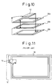
- a contactless IC card as shown in Fig. 11, comprises a semiconductor element 12 for sending and receiving signals, an antenna 10 in the form of a flat coil electrically connected to the semiconductor element 12, and card-like films 14 for holding the antenna 10 and the semiconductor element 12 from the two sides thereof, thereby forming a thin card as a whole.
- the antenna 10 can be formed by pressing a thin metal sheet into a predetermined shape of a coil, or etching a conductive layer formed on one side of a film into a predetermined shape of coil.
- the conventional contactless IC card as shown in Fig. 11, has the antenna 10 arranged along the outer peripheral edge of the card.
- This arrangement is employed in view of the fact that the communication characteristics of the antenna 10 are determined by the area defined by the loop and the number of turns of the antenna, and also under the restraint of the size of a "card", the loop of the antenna 10 is formed along the outer peripheral edge while at the same time taking portability into account.
- the antenna can be formed by pressing or etching a thin metal sheet (e.g. an iron sheet) which is about 0.1 mm thick.
- a thin metal sheet e.g. an iron sheet
- the clearance between one antenna and an adjacent antenna is usually ranges from 0.1 mm to 0.5 mm though it is generally determined by the number of turns of the antenna.
- the surface of the antenna formed as described above can be plated with nickel. Also, the surface of the portions of the antenna to which bonding wires are bonded, to electrically connect a semiconductor element and the antenna, can be plated with gold or palladium.
- the object of the present invention is to provide a semiconductor device, and a preferred method of fabrication thereof, which can reduce the size of the electronic parts having such communication characteristics and are readily applicable to various electronic equipment.
- the present invention is configured as described below.
- a semiconductor device with an antenna comprising one or more antenna units for sending and receiving signals, and a semiconductor element electrically connected to the antenna units, wherein the antenna units are formed by pressing or etching a thin metal sheet with substantially the same flat surface size as the semiconductor element, and the antenna units are integrally coupled to the surface of the semiconductor element.
- the antenna units are formed in a size capable of being arranged within the surface of the semiconductor element and coupled to the surface of the semiconductor element.
- the antenna units are formed in a plurality of layers, separated by insulating layers, and the antenna units formed on the respective layers are electrically connected in series with each other. By adjusting the number of the layers of the antenna unit, the required conditions such as the number of turns of the antenna can be met.
- the outer surface of the antenna is covered with a sealing resin.
- Another feature of this invention is that connecting terminals protruded toward the antenna unit of an adjacent layer are formed on one of the surfaces of antenna units and the antenna units are electrically connected with each other through the connecting terminals.
- the antenna units are electrically connected with each other by using an anisotropic conductive adhesive film or an anisotropic conductive adhesive.
- the use of the anisotropic conductive adhesive film or the anisotropic conductive adhesive facilitates the electrical connection and integration between adjacent antenna layers.
- a method of fabricating a semiconductor device with an antenna comprising one or more antenna units for sending and receiving signals and a semiconductor element electrically connected with the antenna units, comprising the steps of forming a plurality of semiconductor elements at predetermined positions on a semiconductor wafer, forming an antenna frame having a plurality of antenna units at the positions corresponding to the predetermined positions by pressing or etching a thin metal sheet, and setting said semiconductor wafer and said antenna frame in register with each other in an opposed relation to each other in accordance with the positions of said semiconductor elements and said antenna units, coupling by connecting each of said semiconductor elements and the corresponding antenna units with each other electrically, and cutting off said semiconductor wafer and said antenna frame to the profile of each of said semiconductor devices.
- a method of fabricating a semiconductor device with an antenna comprising one or more antenna units for sending and receiving signals and a semiconductor element electrically connected with the antenna units, comprising the steps of forming a plurality of semiconductor elements at predetermined positions on a semiconductor wafer, forming an antenna frames, each of which has a plurality of antenna units at the positions corresponding to the predetermined positions, by pressing or etching a thin metal sheet, forming a multilayered member by integrating said antenna frames, each of which is separated by an adhesive film, and by connecting antenna units of said antenna frames electrically in series with each other, and setting said semiconductor wafer and said multilayered member in register with each other in an opposed relation to each other in accordance with the positions of said semiconductor elements and said antenna units, coupling by connecting each of said semiconductor elements and the corresponding antenna units with each other electrically, and cutting off said semiconductor wafer and said multilayered member to the profile of each of said semiconductor devices.
- the antenna units of the antenna frames are electrically connected in series with each other through the connecting terminals on a surface of the antenna unit formed into protrusions toward a surface of an adjacent antenna unit.
- the outer surface of the antenna frame is covered with a sealing resin before the semiconductor wafer, having the antenna frame, is cut off to the profile of each of the semiconductor devices.
- a semiconductor device with an antenna according to this invention is fabricated in such a manner that one or more antenna units used by being connected to a semiconductor element for sending and receiving signals are produced by pressing or etching a thin metal sheet, and the antenna units are electrically connected to the semiconductor element.
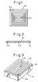
- Fig. 1 shows an example of an antenna unit 20 formed by pressing or etching a thin metal sheet.
- the antenna unit 20 according to this embodiment is designed in such a shape that a coil is laid over the entire surface of the semiconductor element 12.
- the actual operation of working the antenna unit 20 is performed by a method in which a long frame with a multiplicity of pieces of the antenna unit 20 is formed by pressing and each antenna unit 20 is produced from the frame, or by a method in which a frame having a multiplicity of pieces of the antenna unit 20 in two directions is formed by etching so that each antenna unit 20 is produced from this frame.
- Numerals 21a and 21b designate connecting terminals for electrically connecting the antenna unit 20 to the electrode terminals of the semiconductor element 12.
- the connecting terminal 21a is formed at an end of the outer peripheral portion of the antenna unit 20, and the connecting terminal 21b is formed at an end of the inner peripheral portion.
- the connecting terminals 21a and 21b are formed in such a manner as to protrude from the flat surface on which the antenna unit 20 is wound.
- the protrusions can be easily formed in parts of a thin metal sheet punched during the pressing step for forming the coiled antenna unit 20.
- a pattern of the antenna unit 20 is formed by etching the thin metal sheet and the portions to be formed with the connecting terminals 21a and 21b are formed into the protrusions.
- Fig. 2 shows an antenna unit 20 which has an anisotropic conductive adhesive film 16 bonded to the side of the antenna unit 20 from which the connecting terminals 21a and 21b are protruded.
- the anisotropic conductive adhesive film 16 is used for coupling by electrically connecting the antenna unit 20 to the semiconductor element 12.
- Fig. 3 is a perspective view showing the state in which the antenna unit 20 is coupled to the semiconductor element 12 through the anisotropic conductive adhesive film 16, and Fig. 4 is a sectional view of the same.
- connecting pads 13 for coupling with the connecting terminals 21a and 21b of the antenna unit 20 are formed on the surface of the semiconductor element 12 and slightly protrude therefrom.
- the antenna unit 20 to which the anisotropic conductive adhesive film 16 is bonded is set in register with the semiconductor element 12 and, by heating and pressing, the antenna unit 20 is bonded integrally with the semiconductor element 12, while connecting only the connecting pad 13 and the connecting terminals 21a, 21b electrically to each other.
- Fig. 3 shows a semiconductor device with an antenna having the antenna unit 20, which is formed in the same flat shape as the semiconductor element 12, within the surface of the semiconductor element 12.
- This semiconductor device in which the antenna unit 20 is integrally built-in, constitutes a device having a function similar to the conventional contactless IC card. Even in the case where a pattern of the antenna unit 20 is required to be laid with high density within the surface of the semiconductor element 12 to obtain the required communication characteristics, the required antenna pattern can be formed by pressing or etching.
- the outer surface of the antenna unit 20 of the semiconductor device shown in Fig. 3 may be covered with a sealing resin 18 or, as shown in Fig. 5(b), the entire surface of the antenna unit 20 and the semiconductor element 12 may be covered with the sealing resin 18.
- the semiconductor device concerns the case in which the antenna unit 20 is formed in a single layer.
- the single layer cannot provide a sufficient number of turns of the antenna unit 20
- the required number of turns can be obtained by integrating a plurality of the antenna units 20.
- Figs. 6(a) to 6(c) show a method of fabricating a semiconductor device with an antenna comprising a plurality of antenna units integrated and arranged on the surface of the semiconductor element 12.
- Fig. 6(a) shows the state in which anisotropic conductive adhesive films 16 are bonded to the antenna units 20a, 20b and 20c formed with a required pattern by pressing or etching.
- the antenna units 20a, 20b and 20c are each formed with protruded connecting terminals 21 for electrically connecting the layers in which the antenna units 20a, 20b and 20c are set and integrated in register to each other.
- the anisotropic conductive adhesive films 16 are bonded to that side of each of the antenna units 20a, 20b and 20c from which the connecting terminals 21 are projected.
- Fig. 6(b) shows the state in which the antenna units 20a, 20b and 20c with the anisotropic conductive adhesive films 16 bonded thereto are set in register with each other, and by heating and pressing, are integrated into a multilayered member 22.
- the antenna units 20a, 20b and 20c between the adjacent layers are electrically connected to each other with only the portions thereof formed with the connecting terminals 21.
- Fig. 6(c) shows the state in which the multilayered member of the antenna units 20a, 20b and 20c is set in register with and bonded to the semiconductor element 12.
- the anisotropic conductive adhesive film 16 may be used so that the connecting terminals 21 on the adhesive surface of the semiconductor element 12 can be electrically connected and integrated with the connecting pads 13.
- an anisotropic conductive adhesive may be coated to bond the antenna units 20a, 20b and 20c and the antenna multilayered member 22.
- a semiconductor device with antenna units can be obtained with the antenna units 20a, 20b and 20c integrated within the surface of the semiconductor element 12.
- the integration of the antenna units 20a, 20b and 20c can produce a semiconductor device having the same plan as the semiconductor element 12 without enlarging the space in which the antenna units are arranged.
- the antenna units may be integrated in a greater number of layers.
- the integrated antenna units arrangement can produce a semiconductor device having the required communication characteristics.
- the semiconductor device formed using the antenna unit multilayered member 22 constitutes a product having an appearance similar to the semiconductor device shown in Fig. 3.
- the method of fabricating a semiconductor device with antenna according to the embodiments described above is one for fabricating a semiconductor by coupling an antenna unit to each of the semiconductor elements 12 formed individually.
- a semiconductor device with an antenna having the same shape as the semiconductor element as described above can be obtained also by a method in which antenna units are units set in register with and coupled to a semiconductor wafer, after which the semiconductor wafer is cut off in to the device.
- Fig. 7 shows a method of fabricating a semiconductor device with an antenna using a semiconductor wafer 30.
- the semiconductor wafer 30 is formed with semiconductor elements used for sending and receiving signals.
- Numeral 32 designates an antenna frame to be coupled by being electrically connected to each semiconductor element of the semiconductor wafer 30.
- the antenna frame 32 is formed as a large-sized frame in such a manner that each antenna unit 20 is formed into a predetermined pattern in accordance with the arrangement of each semiconductor element of the semiconductor wafer 30 and the adjacent antennas 20 are coupled by tie bars.
- the antenna frame 32 is formed by pressing or etching, and as in the aforementioned case, connecting terminals 21a and 21b are formed on each antenna unit 20.
- the semiconductor wafer 30 and the antenna frame 32 are set in register with each other and, by being heated and pressed through an anisotropic conductive adhesive film 34, the semiconductor 30 is bonded integrally with the antenna frame 32.
- each semiconductor element 12 and the corresponding antenna unit 20 are electrically connected and bonded to each other.
- the semiconductor wafer 30 and the antenna frame 32 after being thus integrally bonded to each other, are sliced at the cutting position of each semiconductor device thereby to produce each semiconductor device with antenna unit.
- the tie bars are cut off so that the antenna unit of each semiconductor device comes to assume an independent form.
- the semiconductor device is obtained as a chip-sized product as in the embodiments described above.
- the outer surface of the antenna frame 32 and the lower surface of the semiconductor wafer 30 are sealed to each other by a sealing resin 18 and then the individual semiconductor devices are cut off, thereby producing a semiconductor device shown in Fig. 8. With this semiconductor device, the outer surface of the antenna unit 20 and the lower surface of the semiconductor element 12 are sealed by the sealing resin 18.
- the aforementioned method of fabricating a semiconductor device with an antenna by coupling the antenna frame 32 to the semiconductor wafer 30 has the advantage that the semiconductor devices can be efficiently fabricated.
- the antenna frame 32 can also be formed efficiently as a large-sized frame by etching thereby contributing to a highly efficient fabrication.
- An individual antenna frame can of course be coupled to each semiconductor element formed on the wafer without using the large-sized antenna frame 32.
- the antenna unit 20 is arranged in the surface of the semiconductor element 12. As shown in Fig. 9, however, the outline of the integrated member 22 formed by integrating the antenna units may be set to a larger size than the semiconductor element 12, so that the semiconductor element 12 is mounted on the integrated member 22.
- the semiconductor element 12 is bonded and mounted on the outer surface of the integrated member 22. Then, the semiconductor element 12 and the antenna 20 are electrically connected by wire bonding.
- Fig. 10 shows antenna patterns formed in the first, second and third layers and a structure for electrically connecting the antenna units 20a, 20b and 20c.
- the antenna units 20a, 20b and 20c are connected in series between the layers through the connecting terminals of each layer.
- the semiconductor element 12 is electrically connected in series to the ends of the antenna units 20a, 20b and 20c.
- the electrical connection between the antenna unit 20 and the semiconductor element 12 can use wire bonding and is not limited to the use of the anisotropic conductive adhesive film 16 by which the connecting terminals and the opposed connecting pads arranged are connected to each other. Also, the connecting terminals and the opposed connecting pads can be connected by solder by way of solder bumps formed on the connecting pads. Also, an ordinary resin adhesive may be used instead of the anisotropic conductive resin film. Further, in the case of the semiconductor device shown in Fig. 9, the outer surface of the antenna unit 20 and the outer surface of the semiconductor element 12 can be sealed with a sealing resin.
- the semiconductor device with an antenna according to this invention is formed with the antenna units by pressing or etching a thin metal sheet and has the advantage that it can be fabricated by using the conventional pressing technique and the conventional etching technique as they are.
- the semiconductor device with an antenna is formed substantially in the same size as the semiconductor element 12 and is therefore very small in size.
- This product can be used as an electronic part much smaller than the conventional IC card by utilization of the communication functions thereof. Also, the smaller size improves the portability, and commercial products easy to carry can be fabricated with a built-in semiconductor device.
- the semiconductor device according to the invention is expected to find wide applications in a variety of fields.
- the semiconductor device with an antenna according to the invention is provided as a product formed substantially in the same size as the semiconductor element.
- This semiconductor device therefore, is expected to find application in contactless types of communications.
- a method of fabricating the semiconductor device according to this invention makes it possible to fabricate a semiconductor device with an antenna both efficiently and easily.
Landscapes
- Engineering & Computer Science (AREA)
- Computer Hardware Design (AREA)
- Microelectronics & Electronic Packaging (AREA)
- Physics & Mathematics (AREA)
- General Physics & Mathematics (AREA)
- Theoretical Computer Science (AREA)
- Computer Networks & Wireless Communication (AREA)
- Credit Cards Or The Like (AREA)
- Dicing (AREA)
- Details Of Aerials (AREA)
- Variable-Direction Aerials And Aerial Arrays (AREA)
Abstract
Description
Claims (10)
- A semiconductor device with an antenna comprising one or more antenna units for sending and receiving signals and a semiconductor element electrically connected to said antenna units,
wherein said antenna units are formed by pressing or etching a thin metal sheet with substantially the same flat surface size as said semiconductor element, and
wherein said antenna units are integrally coupled to the surface of said semiconductor element. - A semiconductor device with an antenna according to claim 1,
wherein said antenna units are formed in a size capable of being arranged within the surface of said semiconductor element and coupled to said surface of said semiconductor element. - A semiconductor device with an antenna according to claim 1 or 2,
wherein said antenna units are formed in a plurality of layers each separated by insulating layers, and the antenna units formed on said respective layers are electrically connected in series with each other. - A semiconductor device with an antenna according to claim 1, 2 or 3,
wherein the outer surface of said antenna is covered with a sealing resin. - A semiconductor device with an antenna according to claim 3,
wherein connecting terminals protruded toward the antenna unit of an adjacent layer are formed on one of the surfaces of antenna units,
wherein said antenna units are electrically connected with each other through said connecting terminals. - A semiconductor device with an antenna according to claim 5,
wherein said antenna units are electrically connected with each other by using an anisotropic conductive adhesive film or an anisotropic conductive adhesive. - A method of fabricating a semiconductor device with an antenna, comprising one or more antenna units for sending and receiving signals and a semiconductor element electrically connected with said antenna units,comprising the steps of forming a plurality of semiconductor elements at predetermined positions on a semiconductor wafer, forming an antenna frame having a plurality of antenna units at the positions corresponding to said predetermined positions by pressing or etching a thin metal sheet, and setting said semiconductor wafer and said antenna frame in register with each other in opposed relation to each other in accordance with the positions of said semiconductor elements and said antenna units, coupling by connecting each of said semiconductor elements and the corresponding antenna units with each other electrically, and cutting off said semiconductor wafer and said antenna frame to the profile of each of said semiconductor devices.
- A method of fabricating a semiconductor device with an antenna, comprising one or more antenna units for sending and receiving signals and a semiconductor element electrically connected with said antenna units,comprising the steps of forming a plurality of semiconductor elements at predetermined positions on a semiconductor wafer, forming an antenna frames, each of which has a plurality of antenna units at the positions corresponding to said predetermined positions, by pressing or etching a thin metal sheet, forming a multilayered member by integrating said antenna frames, each of which is separated by an adhesive film, and by connecting antenna units of said antenna frames electrically in series with each other, and setting said semiconductor wafer and said multilayered member in register with each other in an opposed relation to each other in accordance with the positions of said semiconductor elements and said antenna units, coupling by connecting each of said semiconductor elements and the corresponding antenna units with each other electrically, and cutting off said semiconductor wafer and said multilayered member to the profile of each of said semiconductor devices.
- A method of fabricating a semiconductor device with an antenna according to claim 8,
wherein said antenna units of said antenna frames, each of which is separated by an adhesive film, are electrically connected in series with each other through the connecting terminals on a surface of said antenna unit formed into protrusions toward a surface of an adjacent antenna unit. - A method of fabricating a semiconductor device with an antenna according to claim 7 or 8,
wherein the outer surface of said antenna frame is covered with a sealing resin before said semiconductor wafer, having said antenna frame, is cut off to the profile of each of said semiconductor devices.
Applications Claiming Priority (2)
| Application Number | Priority Date | Filing Date | Title |
|---|---|---|---|
| JP11198618A JP2001024145A (en) | 1999-07-13 | 1999-07-13 | Semiconductor device and manufacturing method thereof |
| JP19861899 | 1999-07-13 |
Publications (2)
| Publication Number | Publication Date |
|---|---|
| EP1069645A2 true EP1069645A2 (en) | 2001-01-17 |
| EP1069645A3 EP1069645A3 (en) | 2002-01-09 |
Family
ID=16394200
Family Applications (1)
| Application Number | Title | Priority Date | Filing Date |
|---|---|---|---|
| EP00305691A Withdrawn EP1069645A3 (en) | 1999-07-13 | 2000-07-06 | Semiconductor device with an antenna and fabrication method therefor |
Country Status (3)
| Country | Link |
|---|---|
| US (1) | US6552694B1 (en) |
| EP (1) | EP1069645A3 (en) |
| JP (1) | JP2001024145A (en) |
Cited By (14)
| Publication number | Priority date | Publication date | Assignee | Title |
|---|---|---|---|---|
| WO2002007260A3 (en) * | 2000-07-19 | 2002-06-06 | Logitech Europ Sa | Three-dimensional geometric space loop antenna |
| WO2005074402A3 (en) * | 2004-02-10 | 2006-01-12 | Cyrips Pte Ltd | An integrated circuit |
| WO2006022836A1 (en) * | 2004-08-06 | 2006-03-02 | International Business Machines Corporation | Apparatus and methods for constructing antennas using wire bonds as radiating elements |
| EP1422658A3 (en) * | 2002-11-21 | 2006-12-13 | Hewlett-Packard Development Company, L.P. | Method of annotating an item with electronic data and apparatus therefor |
| WO2007000245A1 (en) * | 2005-06-24 | 2007-01-04 | Man Roland Druckmaschinen Ag | Direct integration of rfid elements into folding boxes |
| NL1029985C2 (en) * | 2005-09-20 | 2007-03-21 | Sdu Identification Bv | Identity document with chip. |
| EP1788514A1 (en) * | 2005-11-21 | 2007-05-23 | Stmicroelectronics Sa | Electronic micromodule and method of fabrication |
| EP1816591A1 (en) * | 2006-02-03 | 2007-08-08 | Delphi Technologies, Inc. | Antenna arrangement |
| FR2904453A1 (en) * | 2006-07-25 | 2008-02-01 | Oberthur Card Syst Sa | ELECTRONIC ANTENNA WITH MICROCIRCUIT. |
| FR2908207A1 (en) * | 2006-11-03 | 2008-05-09 | Oberthur Card Syst Sa | MICROCIRCUIT CARD, PARTICULARLY OF REDUCED DIMENSION, PROVIDED WITH AN ANTENNA |
| US7586193B2 (en) | 2005-10-07 | 2009-09-08 | Nhew R&D Pty Ltd | Mm-wave antenna using conventional IC packaging |
| FR2940486A1 (en) * | 2008-12-22 | 2010-06-25 | Commissariat Energie Atomique | METHOD FOR MANUFACTURING AN ASSEMBLY OF CHIPS WITH RADIOFREQUENCY TRANSMITTING-RECEPTION MEANS CONNECTED MECHANICALLY BY MEANS OF A RIBBON AND ASSEMBLY |
| CN102780080A (en) * | 2011-05-13 | 2012-11-14 | 吴江华诚复合材料科技有限公司 | Miniaturized ceramic chip antenna |
| EP2926298A1 (en) * | 2012-11-27 | 2015-10-07 | Gemalto SA | Electronic module with three-dimensional communication interface |
Families Citing this family (13)
| Publication number | Priority date | Publication date | Assignee | Title |
|---|---|---|---|---|
| AU2002226093A1 (en) * | 2000-12-15 | 2002-06-24 | Electrox Corp. | Process for the manufacture of novel, inexpensive radio frequency identificationdevices |
| USD502464S1 (en) * | 2003-04-14 | 2005-03-01 | Matsushita Electric Industrial Co., Ltd. | Antenna |
| JP4514497B2 (en) * | 2004-04-12 | 2010-07-28 | パナソニック株式会社 | Manufacturing method of semiconductor device |
| JP4630114B2 (en) * | 2005-04-18 | 2011-02-09 | 新光電気工業株式会社 | Reader / writer and manufacturing method thereof |
| US7398379B1 (en) * | 2005-05-02 | 2008-07-08 | Altera Corporation | Programmable logic device integrated circuits with wireless programming |
| CN100361150C (en) * | 2005-06-24 | 2008-01-09 | 清华大学 | RFID tags with silicon-based integrated antenna |
| JP2007172592A (en) * | 2005-11-25 | 2007-07-05 | Semiconductor Energy Lab Co Ltd | Semiconductor device |
| US7684781B2 (en) * | 2005-11-25 | 2010-03-23 | Semiconductor Energy Laboratory Co., Ltd | Semiconductor device |
| JP2007172198A (en) * | 2005-12-21 | 2007-07-05 | Dainippon Printing Co Ltd | Non-contact data carrier device and files, documents, notebooks and medical records provided with the same |
| JP4848764B2 (en) * | 2005-12-26 | 2011-12-28 | 大日本印刷株式会社 | Non-contact data carrier device |
| JP5023530B2 (en) * | 2006-03-27 | 2012-09-12 | 大日本印刷株式会社 | Non-contact data carrier and wiring substrate for non-contact data carrier |
| TWI380500B (en) * | 2007-02-06 | 2012-12-21 | Mutual Pak Technology Co Ltd | Integrated circuit device having antenna conductors and the mothod for the same |
| FR3073307B1 (en) * | 2017-11-08 | 2021-05-28 | Oberthur Technologies | SECURITY DEVICE SUCH AS A CHIP CARD |
Family Cites Families (7)
| Publication number | Priority date | Publication date | Assignee | Title |
|---|---|---|---|---|
| US4857893A (en) * | 1986-07-18 | 1989-08-15 | Bi Inc. | Single chip transponder device |
| DE9115582U1 (en) * | 1991-12-16 | 1992-12-17 | Siemens AG, 80333 München | PCB antenna |
| DE4306655C2 (en) | 1992-03-04 | 1997-04-30 | Toshiba Kawasaki Kk | Method of manufacturing a planar induction element |
| JP3305843B2 (en) | 1993-12-20 | 2002-07-24 | 株式会社東芝 | Semiconductor device |
| JP2814477B2 (en) | 1995-04-13 | 1998-10-22 | ソニーケミカル株式会社 | Non-contact IC card and method of manufacturing the same |
| FR2753819B1 (en) | 1996-09-20 | 1998-11-27 | INTEGRATED CIRCUIT BOARD WITH MIXED CONNECTION | |
| WO1998006063A1 (en) | 1996-08-02 | 1998-02-12 | Solaic | Integrated circuit card with two connection modes |
-
1999
- 1999-07-13 JP JP11198618A patent/JP2001024145A/en active Pending
-
2000
- 2000-07-06 US US09/609,974 patent/US6552694B1/en not_active Expired - Fee Related
- 2000-07-06 EP EP00305691A patent/EP1069645A3/en not_active Withdrawn
Cited By (25)
| Publication number | Priority date | Publication date | Assignee | Title |
|---|---|---|---|---|
| WO2002007260A3 (en) * | 2000-07-19 | 2002-06-06 | Logitech Europ Sa | Three-dimensional geometric space loop antenna |
| EP1422658A3 (en) * | 2002-11-21 | 2006-12-13 | Hewlett-Packard Development Company, L.P. | Method of annotating an item with electronic data and apparatus therefor |
| US7535359B2 (en) | 2002-11-21 | 2009-05-19 | Hewlett-Packard Development Company, L.P. | Method of annotating an item with electronic data and apparatus therefor |
| WO2005074402A3 (en) * | 2004-02-10 | 2006-01-12 | Cyrips Pte Ltd | An integrated circuit |
| US7295161B2 (en) | 2004-08-06 | 2007-11-13 | International Business Machines Corporation | Apparatus and methods for constructing antennas using wire bonds as radiating elements |
| WO2006022836A1 (en) * | 2004-08-06 | 2006-03-02 | International Business Machines Corporation | Apparatus and methods for constructing antennas using wire bonds as radiating elements |
| WO2007000245A1 (en) * | 2005-06-24 | 2007-01-04 | Man Roland Druckmaschinen Ag | Direct integration of rfid elements into folding boxes |
| US7796042B2 (en) | 2005-06-24 | 2010-09-14 | Man Roland Druckmaschinen Ag | Direct integration of RFID elements into folding boxes |
| WO2007061303A1 (en) * | 2005-09-20 | 2007-05-31 | Sdu Identification B.V. | Identity document comprising a chip |
| NL1029985C2 (en) * | 2005-09-20 | 2007-03-21 | Sdu Identification Bv | Identity document with chip. |
| US8087155B2 (en) | 2005-10-07 | 2012-01-03 | Nhew R&D Pty Ltd | Method of forming an integrated circuit with MM-wave antennas using conventional IC packaging |
| US7586193B2 (en) | 2005-10-07 | 2009-09-08 | Nhew R&D Pty Ltd | Mm-wave antenna using conventional IC packaging |
| FR2893734A1 (en) * | 2005-11-21 | 2007-05-25 | St Microelectronics Sa | ELECTRON MICROMODULE AND METHOD FOR MANUFACTURING SUCH A MICROMODULE |
| EP1788514A1 (en) * | 2005-11-21 | 2007-05-23 | Stmicroelectronics Sa | Electronic micromodule and method of fabrication |
| US7667329B2 (en) | 2005-11-21 | 2010-02-23 | Stmicroelectronics Sa | Electronic micromodule and method for manufacturing the same |
| EP1816591A1 (en) * | 2006-02-03 | 2007-08-08 | Delphi Technologies, Inc. | Antenna arrangement |
| WO2008012416A3 (en) * | 2006-07-25 | 2008-04-03 | Oberthur Card Syst Sa | Electronic entity with microcircuit |
| FR2904453A1 (en) * | 2006-07-25 | 2008-02-01 | Oberthur Card Syst Sa | ELECTRONIC ANTENNA WITH MICROCIRCUIT. |
| WO2008059138A3 (en) * | 2006-11-03 | 2008-10-02 | Oberthur Technologies | Microcircuit card with antenna, particularly having small dimensions |
| FR2908207A1 (en) * | 2006-11-03 | 2008-05-09 | Oberthur Card Syst Sa | MICROCIRCUIT CARD, PARTICULARLY OF REDUCED DIMENSION, PROVIDED WITH AN ANTENNA |
| FR2940486A1 (en) * | 2008-12-22 | 2010-06-25 | Commissariat Energie Atomique | METHOD FOR MANUFACTURING AN ASSEMBLY OF CHIPS WITH RADIOFREQUENCY TRANSMITTING-RECEPTION MEANS CONNECTED MECHANICALLY BY MEANS OF A RIBBON AND ASSEMBLY |
| WO2010072921A1 (en) * | 2008-12-22 | 2010-07-01 | Commissariat A L'energie Atomique Et Aux Energies Alternatives | Method for making an assembly of chips by means of radiofrequency transmission-reception means mechanically connected by a band |
| US8375563B2 (en) | 2008-12-22 | 2013-02-19 | Commissariat A L'energie Atomique Et Aux Energies Alternatives | Method for making an assembly of chips by means of radiofrequency transmission-reception means mechanically connected by a ribbon |
| CN102780080A (en) * | 2011-05-13 | 2012-11-14 | 吴江华诚复合材料科技有限公司 | Miniaturized ceramic chip antenna |
| EP2926298A1 (en) * | 2012-11-27 | 2015-10-07 | Gemalto SA | Electronic module with three-dimensional communication interface |
Also Published As
| Publication number | Publication date |
|---|---|
| US6552694B1 (en) | 2003-04-22 |
| EP1069645A3 (en) | 2002-01-09 |
| JP2001024145A (en) | 2001-01-26 |
Similar Documents
| Publication | Publication Date | Title |
|---|---|---|
| US6552694B1 (en) | Semiconductor device and fabrication method thereof | |
| KR100586049B1 (en) | Integrated circuit boards combined with external contact areas and antennas and their manufacturing processes | |
| JP3557130B2 (en) | Method for manufacturing semiconductor device | |
| JP3238094B2 (en) | Integrated circuit micromodule obtained by a method for continuously assembling strips having a pattern | |
| EP0424530B1 (en) | Resin-sealed semiconductor device | |
| EP0798780A2 (en) | Semiconductor device, manufacturing method thereof and aggregate type semiconductor device | |
| CN100538731C (en) | RFID tag manufacturing method and RFID tag | |
| JP2004265374A (en) | Non-contact communication medium | |
| US8348171B2 (en) | Smartcard interconnect | |
| US7312528B2 (en) | Semiconductor device having antenna connection electrodes | |
| CN108496187B (en) | Method for producing a chip card module and chip card | |
| JP4053231B2 (en) | Wireless communication device | |
| JP2004199114A (en) | IC card, method of manufacturing IC card, and IC module for IC card | |
| KR101151025B1 (en) | Manufacturing method of contact and non-contact card | |
| JPH10157353A (en) | Wireless card and method of manufacturing the same | |
| JP3561117B2 (en) | Wireless module and wireless card | |
| JP3572216B2 (en) | Contactless data carrier | |
| JP2004206736A (en) | Semiconductor device and manufacturing method thereof | |
| JPWO2007057954A1 (en) | Semiconductor device and manufacturing method thereof | |
| JP3557128B2 (en) | Method for manufacturing semiconductor device | |
| KR20010022288A (en) | Ic card and flat coil for ic card | |
| JP2810130B2 (en) | Semiconductor package | |
| US20070132595A1 (en) | Transponder device with mega pads | |
| KR101098289B1 (en) | Rfid tag, method of manufacturing the same, rfid packaging structure using the same and method of manufacturing the rfid packaging structure | |
| JP3483352B2 (en) | Non-contact IC card |
Legal Events
| Date | Code | Title | Description |
|---|---|---|---|
| PUAI | Public reference made under article 153(3) epc to a published international application that has entered the european phase |
Free format text: ORIGINAL CODE: 0009012 |
|
| AK | Designated contracting states |
Kind code of ref document: A2 Designated state(s): AT BE CH CY DE DK ES FI FR GB GR IE IT LI LU MC NL PT SE Kind code of ref document: A2 Designated state(s): DE FR GB |
|
| AX | Request for extension of the european patent |
Free format text: AL;LT;LV;MK;RO;SI |
|
| PUAL | Search report despatched |
Free format text: ORIGINAL CODE: 0009013 |
|
| AK | Designated contracting states |
Kind code of ref document: A3 Designated state(s): AT BE CH CY DE DK ES FI FR GB GR IE IT LI LU MC NL PT SE |
|
| AX | Request for extension of the european patent |
Free format text: AL;LT;LV;MK;RO;SI |
|
| RIC1 | Information provided on ipc code assigned before grant |
Free format text: 7H 01Q 7/00 A, 7H 01Q 1/22 B, 7G 06K 19/077 B, 7H 01Q 1/36 B, 7H 01Q 1/38 B, 7H 01Q 9/27 B |
|
| 17P | Request for examination filed |
Effective date: 20020704 |
|
| AKX | Designation fees paid |
Free format text: DE FR GB |
|
| 17Q | First examination report despatched |
Effective date: 20021018 |
|
| STAA | Information on the status of an ep patent application or granted ep patent |
Free format text: STATUS: THE APPLICATION IS DEEMED TO BE WITHDRAWN |
|
| 18D | Application deemed to be withdrawn |
Effective date: 20031118 |