EP1069476A1 - Belichtungsapparat und Verfahren - Google Patents
Belichtungsapparat und Verfahren Download PDFInfo
- Publication number
- EP1069476A1 EP1069476A1 EP00121341A EP00121341A EP1069476A1 EP 1069476 A1 EP1069476 A1 EP 1069476A1 EP 00121341 A EP00121341 A EP 00121341A EP 00121341 A EP00121341 A EP 00121341A EP 1069476 A1 EP1069476 A1 EP 1069476A1
- Authority
- EP
- European Patent Office
- Prior art keywords
- exposure apparatus
- substrate
- mask
- stage
- wafer
- Prior art date
- Legal status (The legal status is an assumption and is not a legal conclusion. Google has not performed a legal analysis and makes no representation as to the accuracy of the status listed.)
- Withdrawn
Links
- 238000000034 method Methods 0.000 title claims description 17
- 230000003287 optical effect Effects 0.000 claims abstract description 61
- 238000009434 installation Methods 0.000 claims abstract description 43
- 239000000758 substrate Substances 0.000 claims abstract description 42
- 230000007246 mechanism Effects 0.000 claims abstract description 16
- 238000005286 illumination Methods 0.000 abstract description 41
- 235000012431 wafers Nutrition 0.000 description 107
- 239000004065 semiconductor Substances 0.000 description 4
- 238000003384 imaging method Methods 0.000 description 3
- 238000004519 manufacturing process Methods 0.000 description 3
- 230000002411 adverse Effects 0.000 description 2
- 230000005484 gravity Effects 0.000 description 2
- 230000006872 improvement Effects 0.000 description 2
- 239000004973 liquid crystal related substance Substances 0.000 description 2
- 230000009467 reduction Effects 0.000 description 2
- 239000011248 coating agent Substances 0.000 description 1
- 238000000576 coating method Methods 0.000 description 1
- 238000010276 construction Methods 0.000 description 1
- 230000000694 effects Effects 0.000 description 1
- 239000011521 glass Substances 0.000 description 1
- 238000012423 maintenance Methods 0.000 description 1
- 238000012986 modification Methods 0.000 description 1
- 230000004048 modification Effects 0.000 description 1
- 238000000206 photolithography Methods 0.000 description 1
- 229920002120 photoresistant polymer Polymers 0.000 description 1
- 230000008569 process Effects 0.000 description 1
- 230000002035 prolonged effect Effects 0.000 description 1
- 230000003068 static effect Effects 0.000 description 1
Images


Classifications
-
- G—PHYSICS
- G03—PHOTOGRAPHY; CINEMATOGRAPHY; ANALOGOUS TECHNIQUES USING WAVES OTHER THAN OPTICAL WAVES; ELECTROGRAPHY; HOLOGRAPHY
- G03F—PHOTOMECHANICAL PRODUCTION OF TEXTURED OR PATTERNED SURFACES, e.g. FOR PRINTING, FOR PROCESSING OF SEMICONDUCTOR DEVICES; MATERIALS THEREFOR; ORIGINALS THEREFOR; APPARATUS SPECIALLY ADAPTED THEREFOR
- G03F7/00—Photomechanical, e.g. photolithographic, production of textured or patterned surfaces, e.g. printing surfaces; Materials therefor, e.g. comprising photoresists; Apparatus specially adapted therefor
- G03F7/70—Microphotolithographic exposure; Apparatus therefor
- G03F7/70058—Mask illumination systems
-
- G—PHYSICS
- G03—PHOTOGRAPHY; CINEMATOGRAPHY; ANALOGOUS TECHNIQUES USING WAVES OTHER THAN OPTICAL WAVES; ELECTROGRAPHY; HOLOGRAPHY
- G03F—PHOTOMECHANICAL PRODUCTION OF TEXTURED OR PATTERNED SURFACES, e.g. FOR PRINTING, FOR PROCESSING OF SEMICONDUCTOR DEVICES; MATERIALS THEREFOR; ORIGINALS THEREFOR; APPARATUS SPECIALLY ADAPTED THEREFOR
- G03F7/00—Photomechanical, e.g. photolithographic, production of textured or patterned surfaces, e.g. printing surfaces; Materials therefor, e.g. comprising photoresists; Apparatus specially adapted therefor
- G03F7/70—Microphotolithographic exposure; Apparatus therefor
- G03F7/70216—Mask projection systems
- G03F7/70358—Scanning exposure, i.e. relative movement of patterned beam and workpiece during imaging
-
- G—PHYSICS
- G03—PHOTOGRAPHY; CINEMATOGRAPHY; ANALOGOUS TECHNIQUES USING WAVES OTHER THAN OPTICAL WAVES; ELECTROGRAPHY; HOLOGRAPHY
- G03F—PHOTOMECHANICAL PRODUCTION OF TEXTURED OR PATTERNED SURFACES, e.g. FOR PRINTING, FOR PROCESSING OF SEMICONDUCTOR DEVICES; MATERIALS THEREFOR; ORIGINALS THEREFOR; APPARATUS SPECIALLY ADAPTED THEREFOR
- G03F7/00—Photomechanical, e.g. photolithographic, production of textured or patterned surfaces, e.g. printing surfaces; Materials therefor, e.g. comprising photoresists; Apparatus specially adapted therefor
- G03F7/70—Microphotolithographic exposure; Apparatus therefor
- G03F7/70691—Handling of masks or workpieces
- G03F7/70716—Stages
-
- G—PHYSICS
- G03—PHOTOGRAPHY; CINEMATOGRAPHY; ANALOGOUS TECHNIQUES USING WAVES OTHER THAN OPTICAL WAVES; ELECTROGRAPHY; HOLOGRAPHY
- G03F—PHOTOMECHANICAL PRODUCTION OF TEXTURED OR PATTERNED SURFACES, e.g. FOR PRINTING, FOR PROCESSING OF SEMICONDUCTOR DEVICES; MATERIALS THEREFOR; ORIGINALS THEREFOR; APPARATUS SPECIALLY ADAPTED THEREFOR
- G03F7/00—Photomechanical, e.g. photolithographic, production of textured or patterned surfaces, e.g. printing surfaces; Materials therefor, e.g. comprising photoresists; Apparatus specially adapted therefor
- G03F7/70—Microphotolithographic exposure; Apparatus therefor
- G03F7/708—Construction of apparatus, e.g. environment aspects, hygiene aspects or materials
- G03F7/70808—Construction details, e.g. housing, load-lock, seals or windows for passing light in or out of apparatus
- G03F7/70825—Mounting of individual elements, e.g. mounts, holders or supports
Definitions
- the present invention relates to an exposure apparatus for use in producing semiconductor devices and liquid crystal displays.
- a projection exposure apparatus is used for forming a fine circuit pattern on a semiconductor layer or a metallic wiring layer.
- a reticle or a photomask (hereinafter, frequently referred to simply as "reticle") having formed thereon a circuit pattern is provided on a reticle stage, and a wafer stage having provided thereon a semiconductor wafer or a glass substrate (hereinafter, frequently referred to simply as "wafer") with a photoresist coating is moved relative to the reticle along an x-axis and a y-axis in a two-dimensional plane, to thereby transfer the circuit pattern formed on the reticle to a predetermined area on the wafer.
- Types of exposure apparatuses can be roughly classified as a projection exposure apparatus of a step and repeat type in which a pattern on a reticle is projected through a projection optical system as a reduced pattern image and the reduced pattern image is formed on each exposure field on a wafer, and a scanning projection exposure apparatus of a so-called step and scan type in which a part of a pattern on a reticle is projected through a projection optical system on a wafer while moving the reticle and the wafer synchronously in predetermined scanning directions, to thereby transfer the pattern on the reticle to the wafer.
- main components of the exposure apparatus i.e., an illumination optical system, a mask stage and a substrate stage
- main components of the exposure apparatus i.e., an illumination optical system, a mask stage and a substrate stage
- these components are supported relative to an installation surface for the exposure apparatus by four support legs. It is preferred that these components be maintained precisely horizontally. However, it is extremely difficult to maintain these components of the exposure apparatus on a horizontal plane by adjusting the lengths of four support legs, so that dynamic stability of the entire exposure apparatus is likely to be poor. Further, the area of the installation surface for the exposure apparatus, which is included within four support legs, is relatively large.
- the present invention has been made. It is an object of the present invention to provide an exposure apparatus which has an excellent dynamic stability for exposure.
- an exposure apparatus for transferring a pattern of a mask to a substrate comprising:
- an exposure apparatus comprising:
- an exposure apparatus for transferring a pattern of a mask to a substrate comprising:
- a method for supporting an illumination optical system used in an exposure apparatus relative to an installation surface for the exposure apparatus, the illumination optical system having a central axis comprising:
- an exposure method comprising:
- the exposure apparatus of the present invention is supported as a whole at three points, so that the exposure apparatus can be easily adjusted to a datum plane.
- the illumination optical system which has a large weight be supported at a plurality of support points, from the viewpoint of a balance of the entire exposure apparatus.
- the exposure apparatus have an excellent dynamic stability, so that it is preferred that the exposure apparatus be symmetrical with respect to the scanning directions of the mask stage and the substrate stage.
- the conventional exposure apparatus is changed simply by utilizing three support legs, instead of four support legs, in order to ensure that the exposure apparatus is symmetrical with respect to the scanning directions of the mask stage and the substrate stage, problems occur as mentioned below.
- the support leg at the front of the exposure apparatus disturbs conveyance of wafers from the wafer loader to the wafer stage and conveyance of reticles from the reticle loader to the reticle stage. Therefore, it is impossible to minimize a distance for conveying wafers and reticles from the conveying robot to the wafer stage and the reticle stage.
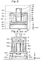
- Fig. 5 shows a conventional projection exposure apparatus viewed from above toward an installation surface therefor.
- Fig. 6 shows a conventional projection exposure apparatus viewed from a front thereof.
- the "front of the projection exposure apparatus” herein means a side of the projection exposure apparatus facing a passage for a conveying robot or the like for conveying a plurality of wafers to a substrate-conveying apparatus (hereinafter, referred to simply as "wafer loader”), which is adjacent to the projection exposure apparatus in a clean room.
- the conveying robot passes through the passage to the wafer loader and supplies the wafers to the wafer loader.
- support legs (hereinafter, referred to as "apparatus-supporting legs") 10a, 10b, 10c and 10d support an apparatus-supporting member 10 relative to the installation surface.
- the apparatus-supporting member 10 supports an entire projection exposure apparatus comprising, as main components, an illumination optical system ILS, a projection optical system PL, a reticle stage RST and a wafer stage WST, which are described later.
- a frame portion (hereinafter, referred to simply as "frame”) of the apparatus-supporting member 10 has a rectangular form as viewed from its top.
- the apparatus-supporting legs 10a, 10b, 10c and 10d are connected to four corner portions of the frame of the rectangular form.
- a coordinate system xyz is defined by an x-axis which is parallel to long sides of the rectangular form of the frame of the apparatus-supporting member 10, a y-axis which is horizontal and perpendicular to the x-axis and a z-axis which is vertical relative to an x-y plane defined by the x-axis and the y-axis.
- the front of the projection exposure apparatus is a visible side when the projection exposure apparatus is viewed in a plus direction of the y-axis.
- the passage for the conveying robot is provided along the x-axis.
- ILS-supporting legs 12a, 12b, 12c and 12d are fixed at their respective ends on the apparatus-supporting member 10. As shown in Fig. 5, the respective fixed ends of the ILS-supporting legs 12a, 12b, 12c and 12d on the apparatus-supporting member 10 constitute four corners of a rectangle. Each of the ILS-supporting legs 12a, 12b, 12c and 12d extends along the z-axis and supports an illumination optical system-supporting member (hereinafter, referred to simply as "ILS-supporting member") 12.
- ILS-supporting member an illumination optical system-supporting member
- a frame of the ILS-supporting member 12 has a rectangular form as viewed from its top and the ILS-supporting legs 12a, 12b, 12c and 12d are connected to four corners of the frame of the rectangular form.
- the ILS-supporting member 12 supports the illumination optical system ILS.
- two short sides determined by the ILS-supporting legs 12a and 12d and the ILS-supporting legs 12b and 12c, respectively are parallel to the y-axis
- two long sides determined by the ILS-supporting legs 12a and 12b and the ILS-supporting legs 12c and 12d, respectively, are parallel to the x-axis.
- the illumination optical system ILS is disposed at the highest position relative to the installation surface.
- An illumination light source and an optical system for obtaining desired illumination light (not shown in the drawings) which extend along the y-axis are provided in the illumination optical system ILS.
- RST-supporting legs 14a, 14b, 14c and 14d are fixed at their respective ends on the apparatus-supporting member 10 inside the rectangle determined by the ILS-supporting legs 12a, 12b, 12c and 12d.
- the respective fixed ends of the RST-supporting legs 14a, 14b, 14c and 14d on the apparatus-supporting member 10 constitute four corners of a rectangle.
- Each of the RST-supporting legs 14a, 14b, 14c and 14d extends along the z-axis and supports a reticle stage-supporting member (hereinafter, referred to simply as "RST-supporting member") 14.
- a frame of the RST-supporting member 14 has a rectangular form as viewed from its top and the RST-supporting legs 14a, 14b, 14c and 14d are connected to four corners of the rectangular frame.
- the rectangle determined by the RST-supporting legs 14a, 14b, 14c and 14d two short sides determined by the RST-supporting legs 14a and 14d and the RST-supporting legs 14b and 14c, respectively, are parallel to the y-axis, and two long sides determined by the RST-supporting legs 14a and 14b and the RST-supporting legs 14c and 14d, respectively, are parallel to the x-axis.
- the RST-supporting member 14 supports the reticle stage RST.
- the reticle stage RST is adapted to move in the x-y plane while having a reticle (not shown in the drawings) provided thereon. During exposure by a so-called step and scan type method, the reticle stage RST is moved along the y-axis. The reticle has formed thereon a predetermined circuit pattern.
- the projection optical system PL is provided below the RST-supporting member 14.
- the projection optical system PL has an optical axis along the z-axis and is supported on the apparatus-supporting member 10.
- the circuit pattern formed on the reticle provided on the reticle stage RST on the RST-supporting member 14 is illuminated with illumination light from the illumination optical system ILS.
- the illumination light passes through the reticle and is collected by the projection optical system PL.
- An image of the circuit pattern on the reticle is formed on an image plane of the projection optical system PL.
- the wafer stage WST is supported on a wafer stage-supporting member (hereinafter, referred to simply as "WST-supporting member") 8.
- the wafer stage WST is adapted to move in the x-y plane while having a wafer in a state such that a surface of the wafer coincides with the above-mentioned image plane of the projection optical system PL.
- the WST-supporting member 8 is provided below the apparatus-supporting member 10 and supported by the apparatus-supporting legs 10a, 10b, 10c and 10d.
- the wafer stage WST is moved along the y-axis synchronously with movement of the reticle stage RST.
- a wafer loader WL is disposed adjacent to the front of the projection exposure apparatus.
- the wafer loader WL takes out a plurality of wafers successively from a wafer library and conveys each wafer to a wafer holder (not shown in the drawings) on the wafer stage WST.
- the projection exposure apparatus, together with the wafer loader WL, is accommodated in a rectangular parallelepiped chamber 20 which is thermostatic.
- each of the apparatus-supporting member 10, the RST-supporting member 14, the ILS-supporting member 12 and the WST-supporting member 8 is supported at four points by four support legs, to thereby support the main components of the exposure apparatus.
- the projection optical system PL is disposed at a position as close to the center (center of gravity) of the exposure apparatus as possible and, in order to move the reticle and the wafer in the x-y plane, especially along the y-axis synchronously, a drive shaft for each of the reticle stage RST and the wafer stage WST is determined as being parallel to a lateral direction or a longitudinal direction of the exposure apparatus, i.e., a direction of the x-axis or a direction of the y-axis in the coordinate system xyz in Figs. 5 and 6.
- auxiliary machines for the illumination optical system ILS and various devices are disposed, such that their long sides are parallel to or perpendicular to the longitudinal direction of the exposure apparatus, that is, a direction of the y-axis.
- a number of exposure apparatuses are installed in a single clean room, so that it is desired that a floor space for installing the exposure apparatus per unit be small, from the viewpoint of costs.
- a chamber in which the conventional exposure apparatuses and the wafer loaders are accommodated must have an area which is slightly larger than the total area of the exposure apparatuses and the wafer loaders, in consideration of a working space for maintenance by an operator. Thus, it is difficult to reduce the floor space for installing the exposure apparatus.
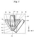
- Fig. 1 shows the exposure apparatus in this embodiment, viewed from above toward an installation surface therefor.
- Fig. 2 shows the exposure apparatus in this embodiment, viewed from a front thereof.
- the "front of the exposure apparatus” means a side of the exposure apparatus facing a passage for allowing a conveying robot or the like to pass therethrough to a wafer loader adjacent to the exposure apparatus in a clean room and supply a plurality of wafers to the wafer loader.
- the exposure apparatus in this embodiment is a scanning projection exposure apparatus of a step and scan type in which a part of a pattern on a reticle is projected through a projection optical system onto a wafer while moving the reticle and the wafer synchronously, to thereby transfer the pattern on the reticle to the wafer.
- an apparatus-supporting member 3 is supported relative to the installation surface at three points by apparatus-supporting legs 3a, 3b and 3c.
- the apparatus-supporting member 3 supports an entire projection exposure apparatus comprising, as main components, an illumination optical system ILS, a projection optical system PL, a reticle stage RST and a wafer stage WST, which are described later.
- a control device 1 is employed to control the entire projection exposure apparatus, especially, to move the reticle stage RST and the wafer stage WST synchronously in opposite directions (the plus and minus directions of the y-axis).
- a frame of the apparatus-supporting member 3 has a substantially isosceles triangular form as viewed from its top, and the apparatus-supporting legs 3a, 3b and 3c are connected to three corner portions of the frame of the substantially isosceles triangular form.
- Each of the apparatus-supporting legs 3a, 3b and 3c has a horizontal cross-section in a substantially square form, and the corner portion of the frame of the apparatus-supporting member 3 is a portion which is cut along one side of the substantially square form of the horizontal cross-section of each of the apparatus-supporting legs 3a, 3b and 3c. Therefore, accurately, the frame of the apparatus-supporting member 3 has a hexagonal form as viewed from its top, as shown in Fig. 1. However, in order to make the present invention to be easily understood by simple explanation, in the following description, it is assumed that the frame of the apparatus-supporting member 3 has an isosceles triangular form as viewed from its top. As shown in Fig.
- a base of the isosceles triangular form of the frame of the apparatus-supporting member 3 is defined by the apparatus-supporting legs 3a and 3c.
- the vertex opposite the base is constituted by the apparatus-supporting leg 3b.
- the side determined by the apparatus-supporting legs 3a and 3b and the side determined by the apparatus-supporting legs 3b and 3c are equal in length.
- a coordinate system xyz is defined by an x-axis which is parallel to one side of the isosceles triangular form of the frame of the apparatus-supporting member 3, a y-axis which is horizontal and perpendicular to the x-axis and a z-axis which is vertical relative to an x-y plane defined by the x-axis and the y-axis.
- the front of the exposure apparatus is a visible side when the exposure apparatus is viewed from the apparatus-supporting leg 3b in the plus direction of the y-axis.
- the passage for the conveying robot is provided along the x-axis and on the side in the minus direction of the y-axis relative to the apparatus-supporting leg 3b.
- the base of the isosceles triangular form which is defined by the apparatus-supporting legs 3a and 3c, is parallel to the x-axis.
- ILS-supporting legs 4a, 4b and 4c are fixed at their respective ends on the apparatus-supporting member 3 in line with or spaced inwardly from the axes of the apparatus-supporting legs 3a, 3b and 3c.
- the respective fixed ends of the ILS-supporting legs 4a, 4b and 4c on the apparatus-supporting member 3 constitute three vertexes of an isosceles triangle.
- Each of the ILS-supporting legs 4a, 4b and 4c extends along the z-axis and supports an ILS-supporting member 4.
- a frame of the ILS-supporting member 4 has a substantially isosceles triangular form as viewed from its top, and the ILS-supporting legs 4a, 4b and 4c are connected to three corner portions of the substantially isosceles triangular form of the frame.
- the frame of the ILS-supporting member 4 has a hexagonal form for the same reasons as mentioned above in connection with the frame of the apparatus-supporting member 3.
- the ILS-supporting member 4 has an isosceles triangular form as viewed from its top.
- the ILS-supporting member 4 supports the illumination optical system ILS.
- a base defined by the ILS-supporting legs 4a and 4c is parallel to the x-axis, and the ILS-supporting leg 4b constituting one vertex opposite the base is located at the front of the exposure apparatus.
- the illumination optical system ILS is disposed at the highest position relative to the installation surface.
- the illumination optical system ILS is disposed at a position such that it is substantially symmetrical with respect to a straight line drawn from the ILS-supporting leg 4b which constitutes one vertex of the isosceles triangle (determined by the ILS-supporting legs 4a, 4b and 4c) toward the middle point between the ILS-supporting legs 4a and 4c defining the base of the isosceles triangle as a side opposite the one vertex constituted by the ILS-supporting leg 4b.
- RST-supporting legs 6a, 6b and 6c are fixed at their respective ends on the apparatus-supporting member 3 inside the isosceles triangle determined by the ILS-supporting legs 4a, 4b and 4c. As shown in Fig. 1, the respective fixed ends of the RST-supporting legs 6a, 6b and 6c on the apparatus-supporting member 3 constitute three vertexes of an isosceles triangle. Each of the RST-supporting legs 6a, 6b and 6c extends along the z-axis and supports an RST-supporting member 6.
- a frame of the RST-supporting member 6 has an isosceles triangular form as viewed from its top and the RST-supporting legs 6a, 6b and 6c are connected to three vertexes of the isosceles triangular form of the frame.
- the frame of the RST-supporting member 6 has a hexagonal form for the same reasons as mentioned above in connection with the frame of the apparatus-supporting member 3.
- it is assumed that the frame of the RST-supporting member 6 has an isosceles triangular form as viewed from its top.
- a base defined by RST-supporting legs 6a and 6c is parallel to the x-axis.
- the RST-supporting member 6 supports the reticle stage RST.
- the reticle stage RST is adapted to move in the x-y plane while having a reticle (not shown in the drawings) provided thereon. During exposure by the step and scan type method, the reticle stage RST is moved in the plus direction of the y-axis.
- the scanning direction of the reticle stage RST is substantially parallel to a straight line drawn from one vertex of the isosceles triangle determined by the three support legs supporting the RST-supporting member toward the middle point in a side opposite the vertex.
- the projection optical system PL is provided below the RST-supporting member 6.
- the projection optical system PL has an optical axis along the z-axis and is supported on the apparatus-supporting member 3.
- the circuit pattern formed on the reticle provided on the reticle stage RST on the RST-supporting member 6 is illuminated with illumination light from the illumination optical system ILS.
- the illumination light passes through the reticle and is collected by the projection optical system PL.
- An image of the circuit pattern on the reticle is formed on an imaging plane of the projection optical system PL.
- the wafer stage WST is supported on a WST-supporting member 8.
- the wafer stage WST is adapted to move in the x-y plane while having a wafer in a state such that a surface of the wafer coincides with the above-mentioned imaging plane of the projection optical system PL.
- the WST-supporting member 8 is provided below the apparatus-supporting member 3 and supported by the apparatus-supporting legs 3a, 3b and 3c.
- the wafer stage WST is moved in the minus direction of the y-axis synchronously with movement of the reticle stage RST.
- the scanning direction of the wafer stage WST is substantially parallel to a straight line drawn from one vertex of the isosceles of the triangle determined by the three support legs supporting the WST-supporting member toward the middle point in a side opposite the vertex.
- a wafer loader WL is disposed adjacent to one side determined by the apparatus-supporting legs 3b and 3c on the right side of the exposure apparatus in Figs. 1 and 2. That is, the wafer loader WL for loading and unloading a wafer with respect to the wafer stage WST is disposed along one side of the isosceles triangle determined by three support legs, as viewed in a vertical direction relative to the installation surface.
- the projection exposure apparatus, together with the wafer loader WL, is accommodated in a chamber 20 which is thermostatic.
- the exposure apparatus in the first embodiment of the present invention is supported as a whole at three points. Therefore, differing from the conventional exposure apparatus which is supported as a whole at four points, wherein cumbersome operations for adjustment of the length of each support leg must be conducted when the exposure apparatus is installed, the exposure apparatus in this embodiment of the present invention can be easily adjusted to a datum plane.
- the wafer stage WST and the reticle stage RST are moved along the x-axis and the y-axis shown in Figs. 1 and 2.
- the illumination optical system ILS which has a large weight and is provided at the highest position in the exposure apparatus, is symmetrical with respect to the y-axis along which the wafer stage WST and the reticle stage RST are moved synchronously during exposure, and is stably supported by two support legs. More particularly, as shown in Fig.
- the illumination optical system ILS is an elongated structure which extends from a central portion of the isosceles triangle determined by three support legs (supporting the ILS-supporting member at three support points) across one side of the isosceles triangle.
- the center of gravity of the illumination optical system ILS is shifted toward one side across which the illumination optical system ILS extends, the weight of a portion of the illumination optical system ILS around that side of the isosceles triangle is satisfactorily stably supported by two support legs.
- the exposure apparatus as a whole is symmetrical with respect to the y-axis along which the wafer stage WST and the reticle stage RST are moved synchronously during exposure, so that the exposure apparatus has an excellent ability to withstand vibration thereof due to movement of the wafer stage WST and the reticle stage RST during exposure.
- the wafer loader WL is not symmetrical with respect to the y-axis at its position. However, because the wafer loader WL can be provided separately from the exposure apparatus, it is possible to prevent the wafer loader WL from adversely affecting the stability of the exposure apparatus.
- a distance between the wafer loader WL and the wafer stage WST is small, so that it has become possible to effectively utilize a space within the exposure apparatus and hence, an improvement in performance of the exposure apparatus and reduction in the floor space for installing the exposure apparatus can be achieved.
- Fig. 3 shows the exposure apparatus in this embodiment, viewed from above toward an installation surface therefor.
- Fig. 4 shows the exposure apparatus in this embodiment, viewed from a front thereof.
- the "front of the exposure apparatus” means a side of the exposure apparatus facing a passage for allowing a conveying robot or the like to pass therethrough to a wafer loader adjacent to the exposure apparatus in a clean room and supply a plurality of wafers to the wafer loader.
- the exposure apparatus in this embodiment is of the same type as that of the exposure apparatus in the first embodiment, that is, a scanning projection exposure apparatus of a step and scan type.
- the members and portions of the exposure apparatus have the same function and effects as those in the first embodiment of the present invention. Therefore, in Figs. 3 and 4, the members and portions of the exposure apparatus are denoted by the same reference numerals as used in the first embodiment of the present invention and descriptions of those members and portions are omitted to avoid overlapping.
- the same coordinate system xyz as used in the first embodiment of the present invention is employed, that is, the coordinate system defined by an x-axis which is parallel to one side of the isosceles triangular form of the frame of the apparatus-supporting member 3, a y-axis which is horizontal and perpendicular to the x-axis and a z-axis which is vertical relative to an x-y plane defined by the x-axis and the y-axis.
- the coordinate system xyz is rotated about the z-axis at a predetermined angle. Therefore, in the second embodiment, the front of the exposure apparatus corresponds to a side determined by the apparatus-supporting legs 3a and 3b, and the passage for the conveying robot is provided in parallel to the side determined by the apparatus-supporting legs 3a and 3b.
- the illumination optical system ILS is disposed at a position such that it is substantially symmetrical with respect to a straight line drawn from the ILS-supporting leg 4b which constitutes one vertex of the isosceles triangle (determined by the ILS-supporting legs 4a, 4b and 4c) toward the middle point between the ILS-supporting legs 4a and 4c determining the base of the isosceles triangle, i.e., a side opposite the vertex constituted by the ILS-supporting leg 4b.
- the reticle stage RST is adapted to move in the x-y plane while having a reticle (not shown in the drawings) provided thereon.
- the reticle stage RST is moved in a direction of the y-axis. That is, as viewed in a direction of the z-axis (i.e., a vertical direction relative to the installation surface), the scanning direction of the reticle stage RST is substantially parallel to a straight line drawn from one vertex of the isosceles triangle determined by the three support legs supporting the RST-supporting member toward the middle point in a side opposite the vertex.
- the wafer stage WST is moved in a direction of the y-axis synchronously with movement of the reticle stage RST. That is, as viewed in a direction of the z-axis (i.e., a vertical direction relative to the installation surface), the scanning direction of the wafer stage WST is substantially parallel to a straight line drawn from one vertex of the isosceles triangle determined by the three support legs supporting the WST-supporting member toward the middle point in a side opposite the vertex.
- a wafer loader WL is disposed adjacent to the side determined by the apparatus-supporting legs 3a and 3b at the front of the exposure apparatus, as shown in Fig. 3. That is, the wafer loader WL for loading and unloading a wafer with respect to the wafer stage WST is disposed along one side of the isosceles triangle determined by three support legs, as viewed in a vertical direction relative to the installation surface.
- the projection exposure apparatus, together with the wafer loader WL, is accommodated in a chamber 20 which is thermostatic.
- One wall surface of the chamber 20 is disposed in parallel to one side of the isosceles triangle determined by the apparatus-supporting legs 3a, 3b and 3c, along which the wafer loader WL is disposed.
- the illumination optical system ILS which has a large weight and is provided at the highest position in the exposure apparatus, is symmetrical with respect to the y-axis along which the wafer stage WST and the reticle stage RST are moved synchronously during exposure, and is stably supported by two support legs. Further, the exposure apparatus is symmetrical as a whole with respect to the y-axis along which the wafer stage WST and the reticle stage RST are moved synchronously during exposure, so that the exposure apparatus has an excellent ability to withstand vibration thereof due to movement of the wafer stage WST and the reticle stage RST during exposure.
- the wafer loader WL is not symmetrical with respect to the y-axis at its position. However, because the wafer loader WL can be provided separately from the exposure apparatus, it is possible to prevent the wafer loader WL from adversely affecting the stability of the exposure apparatus.
- the exposure apparatus in the second embodiment of the present invention is rotated about the z-axis at a predetermined angle relative to the exposure apparatus in the first embodiment of the present invention.
- problems are likely to occur, such that the position of an interface between the wafer loader and a wafer coater/a wafer developer in a production line is limited to one side of the exposure apparatus (e.g., the right side in Fig. 1), leading to a lack of flexibility in arrangement of the production line, and that when a plurality of exposure apparatuses are employed, accessibility of the exposure apparatuses is poor.
- the exposure apparatus in the second embodiment of the present invention is free from these problems.
- the illumination optical system ILS which protrudes backward in the conventional exposure apparatus, is disposed obliquely relative to the front of the exposure apparatus, so that the length of the entire exposure apparatus can be reduced.
- the wafer loader WL can be disposed adjacent to the front of the exposure apparatus as in the conventional exposure apparatus. Therefore, flexibility in installing the exposure apparatus can be ensured. In addition, symmetry of the exposure apparatus can be maintained, so that the exposure apparatus has an excellent dynamic stability.
- the present invention is not limited to the above-mentioned embodiments. Various modifications are possible, as long as they fall within the scope of the present invention defined in the appended claims.
- the present invention is applied to a scanning project exposure apparatus of a so-called step and scan type.
- the present invention may be applied to a projection exposure apparatus of a so-called step and repeat type in which a pattern on a reticle is projected through a projection optical system as a reduced pattern image and the reduced pattern image is formed on each shot area on a wafer.
- the exposure apparatus of the present invention is an exposure apparatus which comprises an illumination optical system ILS for illuminating a reticle, a reticle stage RST for holding thereon the reticle, a projection optical system PL for projecting therethrough a pattern on the reticle and a wafer stage WST for holding thereon a wafer, which is adapted to move along an x-axis and a y-axis in a two-dimensional plane so as to position the wafer at an imaging position of the pattern, and is supported as a whole relative to an installation surface at three points by three support legs, wherein as viewed in a vertical direction relative to the installation surface, either of the x-axis and the y-axis with respect to the wafer stage WST is parallel to a straight line drawn from one vertex of a triangle determined by the three support legs toward the middle point in a side opposite the vertex.
- the three support legs determine an isosceles triangle.
- the support legs may determine a triangle other than an isosceles triangle.
Landscapes
- Physics & Mathematics (AREA)
- General Physics & Mathematics (AREA)
- Health & Medical Sciences (AREA)
- Engineering & Computer Science (AREA)
- Environmental & Geological Engineering (AREA)
- Epidemiology (AREA)
- Public Health (AREA)
- Exposure And Positioning Against Photoresist Photosensitive Materials (AREA)
- Exposure Of Semiconductors, Excluding Electron Or Ion Beam Exposure (AREA)
Applications Claiming Priority (3)
| Application Number | Priority Date | Filing Date | Title |
|---|---|---|---|
| JP9024332A JPH10209035A (ja) | 1997-01-23 | 1997-01-23 | 露光装置 |
| JP2433297 | 1997-01-23 | ||
| EP98300240A EP0855624B1 (de) | 1997-01-23 | 1998-01-14 | Belichtungsapparat und -verfahren |
Related Parent Applications (1)
| Application Number | Title | Priority Date | Filing Date |
|---|---|---|---|
| EP98300240A Division EP0855624B1 (de) | 1997-01-23 | 1998-01-14 | Belichtungsapparat und -verfahren |
Publications (1)
| Publication Number | Publication Date |
|---|---|
| EP1069476A1 true EP1069476A1 (de) | 2001-01-17 |
Family
ID=12135238
Family Applications (2)
| Application Number | Title | Priority Date | Filing Date |
|---|---|---|---|
| EP00121341A Withdrawn EP1069476A1 (de) | 1997-01-23 | 1998-01-14 | Belichtungsapparat und Verfahren |
| EP98300240A Revoked EP0855624B1 (de) | 1997-01-23 | 1998-01-14 | Belichtungsapparat und -verfahren |
Family Applications After (1)
| Application Number | Title | Priority Date | Filing Date |
|---|---|---|---|
| EP98300240A Revoked EP0855624B1 (de) | 1997-01-23 | 1998-01-14 | Belichtungsapparat und -verfahren |
Country Status (4)
| Country | Link |
|---|---|
| US (1) | US6008883A (de) |
| EP (2) | EP1069476A1 (de) |
| JP (1) | JPH10209035A (de) |
| DE (1) | DE69807536D1 (de) |
Families Citing this family (3)
| Publication number | Priority date | Publication date | Assignee | Title |
|---|---|---|---|---|
| US6621556B2 (en) * | 2000-02-28 | 2003-09-16 | Nikon Corporation | Projection exposure apparatus and manufacturing and adjusting methods thereof |
| US6646719B2 (en) * | 2001-01-31 | 2003-11-11 | Nikon Corporation | Support assembly for an exposure apparatus |
| CN119414676B (zh) * | 2024-12-19 | 2025-06-03 | 江苏富港智能科技有限公司 | 一种具有多工位转换机构的曝光机 |
Citations (5)
| Publication number | Priority date | Publication date | Assignee | Title |
|---|---|---|---|---|
| US4226569A (en) * | 1977-04-20 | 1980-10-07 | Thomson-Csf | Wafer loading and positioning device |
| US4786947A (en) * | 1985-01-10 | 1988-11-22 | Canon Kabushiki Kaisha | Projection exposure apparatus |
| US5187519A (en) * | 1990-10-05 | 1993-02-16 | Canon Kabushiki Kaisha | Exposure apparatus having mount means to suppress vibrations |
| GB2299867A (en) * | 1995-04-14 | 1996-10-16 | Nikon Corp | Exposure apparatus |
| WO1996038764A1 (en) * | 1995-05-30 | 1996-12-05 | Philips Electronics N.V. | Lithographic device with a three-dimensionally positionable mask holder |
Family Cites Families (7)
| Publication number | Priority date | Publication date | Assignee | Title |
|---|---|---|---|---|
| DE148911C (de) * | ||||
| NL9100202A (nl) * | 1991-02-05 | 1992-09-01 | Asm Lithography Bv | Lithografische inrichting met een hangende objecttafel. |
| NL9100421A (nl) * | 1991-03-08 | 1992-10-01 | Asm Lithography Bv | Ondersteuningsinrichting met een kantelbare objecttafel alsmede optisch lithografische inrichting voorzien van een dergelijke ondersteuningsinrichting. |
| WO1996038765A1 (en) * | 1995-05-30 | 1996-12-05 | Philips Electronics N.V. | A positioning device with a reference frame for a measuring system |
| TW316874B (de) * | 1995-05-30 | 1997-10-01 | Philips Electronics Nv | |
| TW318255B (de) * | 1995-05-30 | 1997-10-21 | Philips Electronics Nv | |
| JP3659529B2 (ja) * | 1996-06-06 | 2005-06-15 | キヤノン株式会社 | 露光装置およびデバイス製造方法 |
-
1997
- 1997-01-23 JP JP9024332A patent/JPH10209035A/ja active Pending
-
1998
- 1998-01-14 DE DE69807536T patent/DE69807536D1/de not_active Expired - Lifetime
- 1998-01-14 EP EP00121341A patent/EP1069476A1/de not_active Withdrawn
- 1998-01-14 EP EP98300240A patent/EP0855624B1/de not_active Revoked
- 1998-01-21 US US09/010,500 patent/US6008883A/en not_active Expired - Fee Related
Patent Citations (5)
| Publication number | Priority date | Publication date | Assignee | Title |
|---|---|---|---|---|
| US4226569A (en) * | 1977-04-20 | 1980-10-07 | Thomson-Csf | Wafer loading and positioning device |
| US4786947A (en) * | 1985-01-10 | 1988-11-22 | Canon Kabushiki Kaisha | Projection exposure apparatus |
| US5187519A (en) * | 1990-10-05 | 1993-02-16 | Canon Kabushiki Kaisha | Exposure apparatus having mount means to suppress vibrations |
| GB2299867A (en) * | 1995-04-14 | 1996-10-16 | Nikon Corp | Exposure apparatus |
| WO1996038764A1 (en) * | 1995-05-30 | 1996-12-05 | Philips Electronics N.V. | Lithographic device with a three-dimensionally positionable mask holder |
Also Published As
| Publication number | Publication date |
|---|---|
| EP0855624A2 (de) | 1998-07-29 |
| EP0855624A3 (de) | 1998-12-23 |
| DE69807536D1 (de) | 2002-10-10 |
| EP0855624B1 (de) | 2002-09-04 |
| JPH10209035A (ja) | 1998-08-07 |
| US6008883A (en) | 1999-12-28 |
Similar Documents
| Publication | Publication Date | Title |
|---|---|---|
| JP7384242B2 (ja) | 露光装置、露光方法、フラットパネルディスプレイの製造方法、及びデバイス製造方法 | |
| TWI744251B (zh) | 曝光裝置、平面顯示器之製造方法、元件製造方法、及曝光方法 | |
| US20110244396A1 (en) | Exposure apparatus, exchange method of object, exposure method, and device manufacturing method | |
| JP6791154B2 (ja) | 露光装置、フラットパネルディスプレイの製造方法、及びデバイス製造方法 | |
| CN1469193B (zh) | 载台装置及曝光装置 | |
| TWI765918B (zh) | 搬運裝置、曝光裝置、曝光方法、平板顯示器的製造方法、元件製造方法以及搬運方法 | |
| TW202030827A (zh) | 物體搬送裝置、曝光裝置、平面顯示器之製造方法、及元件製造方法 | |
| TWI726917B (zh) | 曝光裝置及曝光方法、以及平面顯示器製造方法 | |
| TWI784440B (zh) | 曝光裝置、平面顯示器之製造方法、元件製造方法、及曝光方法 | |
| US10935894B2 (en) | Movable body apparatus, exposure apparatus, manufacturing method of flat-panel display and device manufacturing method, and movement method of object | |
| JP2013051237A (ja) | 物体処理装置、フラットパネルディスプレイの製造方法、デバイス製造方法、物体搬送装置、及び物体の搬入方法 | |
| JP2005092137A (ja) | 露光装置及び露光方法 | |
| US6008883A (en) | Apparatus and method for exposure | |
| JPH09148219A (ja) | 基板アダプタ | |
| KR102549056B1 (ko) | 노광 장치, 플랫 패널 디스플레이의 제조 방법, 디바이스 제조 방법, 및 노광 방법 | |
| JP2012238776A (ja) | 物体交換システム、露光装置、フラットパネルディスプレイの製造方法、デバイス製造方法、及び物体交換方法 | |
| JP2001332600A (ja) | 搬送方法、露光装置 | |
| JP2008227424A (ja) | 露光装置及びデバイス製造方法 | |
| JP6015983B2 (ja) | 物体交換システム、露光装置、フラットパネルディスプレイの製造方法及びデバイス製造方法 | |
| CN108139679A (zh) | 曝光装置、平面显示器的制造方法、组件制造方法、及曝光方法 | |
| JPH11249317A (ja) | 露光装置 | |
| JPH11145048A (ja) | 露光装置 | |
| HK1231184A1 (en) | Exposure apparatus, exchange method of object, exposure method, and device manufacturing method | |
| HK1179750B (en) | Exposure apparatus, exchange method of object, exposure method, and device manufacturing method | |
| KR20080054642A (ko) | 트윈 스캔 노광설비 및 그의 노광방법 |
Legal Events
| Date | Code | Title | Description |
|---|---|---|---|
| PUAI | Public reference made under article 153(3) epc to a published international application that has entered the european phase |
Free format text: ORIGINAL CODE: 0009012 |
|
| 17P | Request for examination filed |
Effective date: 20001030 |
|
| AC | Divisional application: reference to earlier application |
Ref document number: 855624 Country of ref document: EP |
|
| AK | Designated contracting states |
Kind code of ref document: A1 Designated state(s): DE FR GB IT NL |
|
| AKX | Designation fees paid |
Free format text: DE FR GB IT NL |
|
| 17Q | First examination report despatched |
Effective date: 20030826 |
|
| GRAP | Despatch of communication of intention to grant a patent |
Free format text: ORIGINAL CODE: EPIDOSNIGR1 |
|
| STAA | Information on the status of an ep patent application or granted ep patent |
Free format text: STATUS: THE APPLICATION IS DEEMED TO BE WITHDRAWN |
|
| 18D | Application deemed to be withdrawn |
Effective date: 20070210 |