EP1066680B1 - Generateur de predistorsion - Google Patents
Generateur de predistorsion Download PDFInfo
- Publication number
- EP1066680B1 EP1066680B1 EP99907736A EP99907736A EP1066680B1 EP 1066680 B1 EP1066680 B1 EP 1066680B1 EP 99907736 A EP99907736 A EP 99907736A EP 99907736 A EP99907736 A EP 99907736A EP 1066680 B1 EP1066680 B1 EP 1066680B1
- Authority
- EP
- European Patent Office
- Prior art keywords
- signal
- order
- circuit
- input
- input signal
- Prior art date
- Legal status (The legal status is an assumption and is not a legal conclusion. Google has not performed a legal analysis and makes no representation as to the accuracy of the status listed.)
- Expired - Lifetime
Links
Images


Classifications
-
- H—ELECTRICITY
- H03—ELECTRONIC CIRCUITRY
- H03F—AMPLIFIERS
- H03F1/00—Details of amplifiers with only discharge tubes, only semiconductor devices or only unspecified devices as amplifying elements
- H03F1/32—Modifications of amplifiers to reduce non-linear distortion
- H03F1/3241—Modifications of amplifiers to reduce non-linear distortion using predistortion circuits
- H03F1/3258—Modifications of amplifiers to reduce non-linear distortion using predistortion circuits based on polynomial terms
Definitions
- This invention relates to a circuit for deriving a third order signal from an input signal.
- the invention relates to a circuit for use in a polynomial predistorter.
- a linear amplifier provides uniform gain throughout its dynamic range in order that the output signal of the amplifier is a correct, amplified version of the input signal.
- all linear amplifiers exhibit non-ideal properties such as amplitude and phase distortion, which are undesirable and can seriously deteriorate the performance of a system.
- One effect of this non-linearity of the amplifier is the generation of output frequencies equal to the sums and differences of integer multiples of the input frequency components. This effect is known as intermodulation distortion (IMD) and is particularly undesirable in high-power radio frequency (RF) amplifiers designed for use in broadband systems.
- IMD intermodulation distortion
- RF radio frequency
- a broadband amplifier used in the TDMA cellular system will generate various intermodulation products as a result of amplifying a multitude of TDMA channels occurring at fixed frequency intervals across a TDMA band, with coincident active frames.
- a number of linearisation techniques have been developed to overcome the above distortion problems associated with a linear amplifier.
- a few of these techniques operate in real-time to account for time dependent changes in the non-linear characteristics of the amplifier. Such changes may result from, for example, temperature variations in the amplifier, aging of amplifier components, power supply fluctuations, or, most importantly, the input carriers.
- RF-based linearisation techniques the two most commonly used are feed forward linearisation and predistorter linearisation.
- a feed forward linearisation mechanism relies on creating an error signal representative of the IMD products introduced by the linear amplifier, and feeding this signal forward to combine with the output spectrum of the amplifier, cancelling out the unwanted distortion.
- the mechanism In order for the cancellation process to operate correctly, it is necessary for the mechanism to accurately adjust the amplitude and phase of the error signal prior to combining it with the output of the amplifier. This typically involves the use of additional amplifiers and lossy delay lines and couplers appearing in the output path from the main amplifier. These losses and the requirement for additional amplifiers, which are not adding to the output power of the system, result in a low-efficiency solution.
- predistortion linearisation mechanisms involve deliberate alteration of the relatively low level input signal to the amplifier in anticipation of the undesired distortion process occurring within the amplifier. Specifically, the mechanism predistorts the input signal in a inverse sense to the distortion produced by the amplifier such that in series the overall distortion is minimised. Accordingly, the transfer characteristic of the predistorter is approximated as closely as possible to the inverse or complementary function of the transfer characteristic of the amplifier. If the linear amplifier is compressive, i.e. the gain tails off at higher power levels, then the predistorter will compensate for this compression by correspondingly expanding the input signal.
- One approach approximates the inverse function with the exponential characteristics of a diode.
- One or more diodes may be used together with appropriate biasing to achieve a reduction of the distortion in the order of 10 dB.
- a second approach is to perform a piece-wise approximation of the inverse function using a series of linear gain, straight line elements interconnected end-to-end.
- a drawback with this approach is that the alignment and control of the line elements requires complex circuitry owing to the interconnection points having two degrees of freedom.
- the term a is an offset which may be set to zero in a practical polynomial predistorter.
- the term bx represents the gain of the predistorter which is linear and merely contributes to the gain of the main amplifier.
- the terms containing even powers of x represent harmonic distortion components generated in the main amplifier which may be removed using frequency filtering, and therefore these terms may also be set to zero.
- the remaining terms containing odd powers of x represent in-band distortion caused by the main amplifier (in addition to harmonics which can be filtered as above). In fact, each of these odd-power terms may be considered to represent the equivalent order of intermodulation distortion generated in the main amplifier.
- a circuit implementing this approach is disclosed in DE-A-2 306 294.
- a circuit for deriving a third order signal from an input signal comprising input means for providing an input signal to the circuit along first, second and third paths, means for combining the input signal from the first and second paths to produce a second order signal on a squared signal path, means for low-pass filtering the second order signal to remove components at the frequency of the input signal and harmonics thereof, and means for combining the filtered second order signal from the squared signal path with the input signal from the third path to produce a third order signal.
- a circuit in accordance with the first aspect of the present invention provides the advantage that the third order signal generation may take place using relatively low frequency technology to combine the second and first order signals.
- the generation of second and third order signals may also enable the generation of higher-order terms of distortion component such as fifth or seventh order.
- the input signal is a radio frequency (RF) signal which may contain a plurality of channels across a signal bandwidth.
- RF radio frequency
- the third order signal is provided as a third order distortion component at an output of the circuit.
- the circuit further comprising means for providing the second order signal along a second squared path, and means for combining the second order signal from the second squared path with the third order signal to produce a fifth order signal.
- the circuit is for deriving a fifth order signal from an input signal, whereby the input means provides the input signal along fourth and fifth paths, and further comprises means for combining the input signal from the fourth path with the third order signal to produce a fourth order signal, and means for combining the input signal from the fifth path with the fourth order signal to produce a fifth order signal.
- a similar approach may be used in the generation of a seventh order distortion component at an output of the circuit.
- the third order signal may contain input signal energy.
- the fifth order signal may contain both input signal energy and third order signal energy.
- the circuit further comprising means for injecting a direct current (DC) signal either directly into at least one of the signal paths and/or into at least one of the means for combining the signals.
- DC direct current
- the effect of the DC signal is to remove input signal energy from the third order signal, or to remove input signal energy and third order signal energy from the fifth order signal.
- the DC signal is ideally injected into the squared path to add to the second order signal.
- the DC signal may also be injected in the first, second or third paths to achieve the same effect.
- the DC signal is ideally injected into the second squared path to add to the second order signal.
- the DC injection may be controlled (maintained) by an error correction or feedback loop.
- the feedback loop is arranged so as to optimise removal of unwanted signal energies which occur in the third and fifth order signals.
- the feedback loop makes use of digital signal processing (DSP) techniques to reduce the effect of DC offsets produced by analogue components.
- DSP digital signal processing
- the means for combining may be a mixer or a multiplier, and the means for providing a signal along more than one path may include at least one splitter for splitting an incoming signal.
- a multiple order polynomial predistorter 200 having an input for receiving an RF input signal and an output for supplying a predistorted signal to an RF power amplifier 100.
- the RF input signal received at the input of the predistorter is split by the splitter 205 between two channels or paths, the main path 210 supplying the main RF input signal for subsequent amplification, and the distortion path 215 supplying multiple orders of distortion for adding to the main RF input signal.
- the main RF input signal from the main path 210 and the distortion signal from the distortion path 215 are summed in the adder 220 prior to being amplified in the RF power amplifier 100.
- the main path includes a time delay component 225 to ensure that the main RF signal and the distortion signal coincide at the adder 220.
- the output signal from the RF power amplifier 100 will represent a linearly amplified version of the RF input signal as discussed previously.
- An example of a possible RF input signal in the form of two closely spaced frequency tones is shown in Figure 11a.
- the RF signal entering the distortion path 215 is fed into a distortion generation circuit 230 which operates on the RF input signal to generate a set of non-linear distortion components each corresponding to a particular order of distortion.
- the orders of distortion generated at the three output paths of the distortion generation circuit 230 are third order, fifth order, and seventh order, illustrated as frequency spectra in Figures 11b, 11c and 11d respectively. It is also possible for the distortion generation circuit to generate higher order distortion components such as ninth order, or to generate only third order, or third and fifth order distortion components.
- the signals output from the distortion generating circuit 230 are independently adjusted in phase by the set of variable phase-shift components 235 to compensate for any differing phase shifts occurring in the distortion generating circuit 230.
- the distortion signals are then independently adjusted in amplitude by the set of variable attenuators 240.
- the amplitude adjustment ensures that the relative levels of the separate distortion components are set to correctly correspond to the relative levels of the orders of distortion generated intrinsically in the RF power amplifier 100.
- the correctly adjusted signals representing the third, fifth and seventh orders of distortion are then summed in the adder 245 to produce a single multiple order distortion signal.
- This signal is fed into an RF amplifier 250 which controls the level of the multiple order distortion signal relative to the main RF signal on the main path 210.
- FIG 2 shows a block diagram of a circuit for generating a third order distortion component.
- the RF input signal entering the circuit is split three ways by the splitter 405.
- One of the RF signals is then fed into the first input of a mixer or multiplier 410 via a directional coupler 415.
- the directional coupler samples a portion of the RF signal which is fed into the second input of the mixer 410 via an attenuator 420.
- the output of the mixer 410 ideally generates a squared RF signal which contains frequency components in a DC zone, i.e. at low frequencies, and frequency components in a first harmonic zone, i.e. at double the original frequencies.
- the frequency spectra of the squared RF signal is represented in Figure 11e.
- the squared RF signal output from the mixer 410 is then fed into the first input of a mixer 425 via an attenuator 430 and a DC injection summer 435.
- Another RF input signal from the splitter forms the second input to the mixer 425 and may be supplied via a path 440 including a time delay element (not shown) to ensure that the two mixer input signals are in phase.
- the output of the mixer 425 ideally produces a pure cubic signal.
- the frequency spectra of the cubed RF signal is represented in Figure 11f (after filtering to eliminate the DC-zone, harmonic and third harmonic components)
- the cubed RF signal should, ideally, consist of only input RF signal energy, plus in-band third-order components. In practice however other higher orders of in-band distortion will also be present in the output of the mixer 425, together with more input signal energy than would be expected from a theoretical analysis.
- the attenuation values for the attenuators 420 and 430, and the coupling factor for the coupler 415 are chosen to optimise performance with the type of mixers 410 and 425. Optimum performance is a compromise between minimising the unwanted input signal energy, caused by leakage through the mixers, and minimising the higher orders of in-band distortion, caused by non-ideal performance of the mixers 410 and 425.
- the squared RF signal output from the mixer 410 is filtered before entering the mixer 425.
- This enables selection of either the DC zone frequency components of the squared RF signal by means of a low pass filter (as illustrated: LPF432), or the second harmonic zone frequency components of the squared RF signal by means of a high pass filter.
- LPF432 low pass filter
- LPF432 the second harmonic zone frequency components of the squared RF signal by means of a high pass filter.
- Each selection scheme has its own particular benefits, however, both schemes advantageously provide attenuation of the input tone energy at the output, when used in conjunction with the DC-based input tone rejection mechanism described below.
- the selection of the DC zone in practice provides a better behaved response in terms of gain and phase flatness than the second harmonic zone and as a result can provide better coherence between the two third order distortion components shown in Figure 11b.
- the gain and phase flatness of the second harmonic zone version is effected by the high frequency response of the circuit elements, this version has the benefit of producing a output spectrum in which the input tone level is at a similar level to the third order distortion components, without additional correction.
- an alternative position for DC injection could be into the path 440 carrying the RF input signal to the mixer 425.
- the DC signal would then cancel any leakage of a spurious RF input signal present in the squared RF signal resulting from leakage through the mixer 410.
- DC signal injection may also be possible in the signal paths leading to the mixer 410.
- the distortion generation circuit therefore includes an automatic control mechanism 445 for initialising, maintaining, and controlling the DC signal at the correct level for maximum cancellation of the input signal energy.
- the automatic control mechanism operates using a feedback loop principle.
- the output of the distortion generation circuit is sampled by a splitter 450 and is fed into an input of the control mechanism.
- a second input of the control mechanism receives an RF input signal from the splitter 405, preferably via a time delay element (not shown), and functions as a reference signal for the RF input.
- the automatic control mechanism compares the sample from the output with the RF input reference signal, and provides as an output a DC signal level dependent on the level of RF input energy detected in the output sample.
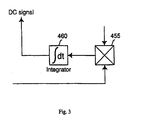
- Figure 3 shows one implementation of the automatic control mechanism in which a detection mixer 455 receives at one input the sample of the output signal and at another input the reference input signal.
- the detection mixer outputs a signal containing components across a range of frequencies. However, the output of the detection mixer of interest is the DC signal component, which provides a measure of the overlap of the unwanted input signal energy in the output with the reference input signal.
- This DC output is isolated from the other signal components in the detection mixer output by integration of the output in the integrator 460.
- the integrator has a time constant long enough to remove the unwanted non-DC signal components but short enough to provide millisecond response in the feedback.
- the DC output of the integrator provides the DC signal for injection into the adder 435.
- a drawback with this control mechanism is that the detection mixer and the integrator may generate DC offset signals which become dominant over the feed back control DC signals. This typically occurs when the level of rejection of the input energy is in the order of 10 - 15 dB. It is possible to use more accurate mixers and integrators to achieve lower DC offsets to counteract this effect. However, mixers and integrators of this kind tend to be rarer and more expensive.
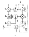
- FIG 4 shows a modified automatic control mechanism which incorporates offset frequency and digital signal processing (DSP) techniques to eliminate the DC offset problem referred to above.
- DSP digital signal processing
- the automatic control mechanism includes the same two inputs and one output as the circuit of Figure 3, and operates as follows.
- a low frequency (LF) fixed oscillator 465 operating in the digital domain of a digital signal processor (DSP) 470 provides via a digital-to-analogue converter 475 a low frequency tone signal to an input of a mixer 480.
- the LF tone signal is ideally at an audio frequency f LF of between 1 and 5 kHz.
- the second input to the mixer 480 is the output sample supplied by the splitter 450 shown in Figure 2, and contains signal components at a relatively higher frequency than the LF tone signal, e.g. between 500 to 2000 MHz.
- the effect of mixing the output sample with the LF tone signal is to generate an image of the output sample shifted down in frequency by f LF and an image of the output sample shifted up in frequency by f LF .
- the output of the mixer 480 is processed by a high pass filter 485 which has a cutoff frequency chosen such that the filter 485 removes any LF tone signal leaking through the mixer 480.
- the frequency offset output sample is then fed into an input of a detection mixer 490, whilst a second input receives the reference RF input signal.
- the detection mixer 490 provides at its output a signal containing components across a range of frequencies. However, in this mechanism it is the signal component at the tone frequency f LF which provides a measure of the overlap of the unwanted input signal energy in the output with the reference input signal.
- the signal After converting the output of the detection mixer 490 back into the digital domain of the digital signal processing (DSP) using the analogue-to-digital converter 495, the signal is fed into a digital mixer 500.
- the digital signal processor and the analogue-to digital converter are ideally suited to dealing with signals at audio frequency and can therefore accurately process the required signal component at the tone frequency f LF .
- the digital mixer 500 mixes the output of the detection mixer 490 with the LF tone signal from the LF fixed oscillator 465 to convert the required signal component also at the tone frequency to a DC signal. As in the mechanism of Figure 3, this DC signal is isolated from the other signal components produced in the detection mixer by integration of the digital mixer output in a digital integrator 505.
- this offset-frequency mechanism is immune to any build up of spurious DC signals in the analogue domain, i.e. in the mixers 480, 490, the D/A 475, the A/D 495 and the high-pass filter 485.
- the potentially damaging DC signals enter the digital signal processor via the analogue to digital converter (A/D) 495, but are immediately converted to the tone signal frequency f LF by the digital mixer 500 and are subsequently cancelled in the integrator 505.
- the digital mixer 500 and the integrator 505 both operate in the digital domain of the digital signal processor (DSP) they do not experience the problems of their analogue counterparts such as signal leakage or spurious DC offset generation due to temperature or power supply fluctuations.
- the DC signal output from the integrator provides via the digital-to-analogue converter 510 the DC signal for injection into the adder 435 of Figure 2.
- Figures 5 and 6 are block diagrams of two alternative embodiments of a circuit for generating third and fifth order distortion components, and are based on the design and basic principles of operation of the third order generation circuit of Figure 2. Like components have therefore been labelled with like references.
- the second order signal is divided into a second path 515 by a splitter 520, and the third order signal is divided into a second path 525 by a splitter 530.
- the second order signal level on the path 515, and the third order signal level on the path 525, are adjusted by an RF amplifier 535 and an attenuator 540 respectively.
- the adjusted second and third order signals are then mixed in the mixer 545 to produce a fifth order RF output.
- a second DC injection signal is added to the second order signal path 515 for mixing with the third order signal on the path 525.
- the RF input signal is further divided by a splitter 550 into paths 555 and 560, and the third order signal is divided by a splitter 530 into a path 525.
- the third order signal is suitably attenuated by attenuators 565 and 570 which in turn feed the mixers 575 and 580.
- the mixers 575 and 580 mix the third order signal with the RF input signals on the paths 555 and 560 respectively.
- the output of the first mixer 575 generates a fourth order signal
- the output of the second mixer 580 generates the fifth order distortion signal for outputting.
- Figure 7 shows the circuit of Figure 5 with a feedback control mechanism which controls and maintains the second DC injection to the adder.
- This feedback control mechanism performs in a similar way as in the third order generation circuit, except that a sample of the fifth order output is compared with a reference signal sampled from the third order output.
- the feedback DC signal therefore provides a measure of the overlap of both the unwanted input signal energy and third order signal energy in the fifth order output.
- the feedback control mechanism may be implemented using the feedback circuits of Figures 3 or 4.
- Figure 8 is a block diagram showing a third order and a fifth order distortion generation circuit with a combined control.
- the circuit is a combination of the third order generation circuit of Figure 2 and the fifth order generation circuit of Figure 7.
- the combined feedback control mechanism for this circuit is shown in Figure 9 and is based on the offset frequency mechanism of Figure 4.
- Figure 10 is a block diagram showing a circuit for generating a seventh order distortion signal based on the principle used in the fifth order generation circuit of Figure 5.
- the fifth order signal is combined with the second order signal to generate a seventh order distortion output.
Landscapes
- Physics & Mathematics (AREA)
- Algebra (AREA)
- General Physics & Mathematics (AREA)
- Mathematical Analysis (AREA)
- Mathematical Optimization (AREA)
- Pure & Applied Mathematics (AREA)
- Nonlinear Science (AREA)
- Engineering & Computer Science (AREA)
- Power Engineering (AREA)
- Amplifiers (AREA)
Claims (18)
- Circuit pour dériver un signal de troisième ordre à partir d'un signal d'entrée, comportant des moyens d'entrée (405) pour délivrer un signal d'entrée au circuit le long de premier, deuxième et troisième trajets, des moyens (410) pour combiner le signal d'entrée provenant des premier et deuxième trajets afin de produire un signal de deuxième ordre sur un trajet de signal élevé au carré, des moyens pour réaliser un filtrage passe-bas du signal de deuxième ordre pour supprimer des composantes à la fréquence du signal d'entrée et à des harmoniques de celle-ci, et des moyens (425) pour combiner le signal de deuxième ordre filtré provenant du trajet de signal élevé au carré avec le signal d'entrée provenant du troisième trajet afin de produire un signal de troisième ordre.
- Circuit selon la revendication 1, pour dériver de plus un signal de cinquième ordre à partir d'un signal d'entrée, comportant en outre des moyens pour délivrer le signal de deuxième ordre le long d'un deuxième trajet de signal élevé au carré (515), et des moyens (545) pour combiner le signal de deuxième ordre provenant du deuxième trajet de signal élevé au carré avec le signal de troisième ordre afin de produire un signal de cinquième ordre.
- Circuit selon la revendication 1, pour dériver de plus un signal de cinquième ordre à partir d'un signal d'entrée, dans lequel les moyens d'entrée délivrent le signal d'entrée le long de quatrième (555) et cinquième (560) trajets, et comportent en outre des moyens pour combiner le signal d'entrée provenant du quatrième trajet avec le signal de troisième ordre afin de produire un signal de quatrième ordre, et des moyens (550) pour combiner le signal d'entrée provenant du cinquième trajet avec le signal de quatrième ordre afin de produire un signal de cinquième ordre.
- Circuit selon l'une quelconque des revendications précédentes, dans lequel le signal d'entrée est un signal radiofréquence.
- Circuit selon l'une quelconque des revendications précédentes, comportant en outre des moyens pour injecter un signal à courant continu dans au moins l'un des trajets de signal.
- Circuit selon la revendication 5, dans lequel les moyens d'injection de courant continu sont agencés pour injecter le signal à courant continu dans le trajet de signal élevé au carré pour l'ajouter au signal de deuxième ordre afin d'annuler l'énergie du signal d'entrée dans le signal de troisième ordre.
- Circuit selon la revendication 6, comportant en outre des moyens de correction d'erreur agencés pour comparer le signal de troisième ordre au signal d'entrée afin de produire un signal de correction d'erreur pour commander l'injection du signal à courant continu dans le trajet de signal élevé au carré.
- Circuit selon la revendication 7, dans lequel les moyens de correction d'erreur sont agençés pour transposer la fréquence du signal de troisième ordre par un signal d'oscillation avant la corrélation avec le signal d'entrée afin de produire un signal de corrélation qui est traité dans un processeur de signaux numériques par comparaison au signal d'oscillation afin de produire le signal de correction d'erreur.
- Circuit selon la revendication 5, comportant en outre des moyens pour injecter le signal à courant continu dans le deuxième trajet de signal élevé au carré pour l'ajouter au signal de deuxième ordre afin d'annuler l'énergie du signal d'entrée et l'énergie du signal de troisième ordre dans le signal de cinquième ordre.
- Circuit selon la revendication 7, comportant de plus des moyens de correction d'erreur agencés pour comparer le signal de cinquième ordre au signal de troisième ordre afin de produire un signal de correction d'erreur pour commander l'injection du signal à courant continu dans le deuxième trajet de signal élevé au carré.
- Circuit selon l'une quelconque des revendications précédentes, dans lequel les moyens de combinaison sont des mélangeurs ou des multiplieurs.
- Circuit selon l'une quelconque des revendications précédentes, dans lequel les moyens d'entrée comportent au moins un diviseur pour délivrer le signal d'entrée le long des trajets de signal.
- Circuit selon l'une quelconque des revendications précédentes, dans lequel les moyens d'entrée comportent au moins un coupleur directif pour délivrer le signal d'entrée le long des trajets de signal.
- Générateur de prédistorsion polynomial incluant un circuit selon la revendication 1.
- Procédé de dérivation d'un signal de prédistorsion de troisième ordre à partir d'un signal d'entrée, comportant la délivrance d'un signal d'entrée à un circuit le long de premier, deuxième et troisième trajets, la combinaison du signal d'entrée provenant des premier et deuxième trajets pour produire un signal de deuxième ordre sur un trajet de signal élevé au carré, le filtrage passe-bas du signal de deuxième ordre pour supprimer des composantes à la fréquence du signal d'entrée et à des harmoniques de celle-ci, et la combinaison du signal de deuxième ordre filtré provenant du trajet de signal élevé au carré avec le signal d'entrée provenant du troisième trajet afin de produire un signal de troisième ordre.
- Circuit selon l'une quelconque des revendications 1 à 13, comportant en outre des moyens pour créer au moins un signal supplémentaire distinct d'ordre impair, chacun desdits signaux supplémentaires distincts d'ordre impair étant créé en combinant le signal d'entrée à lui-même.
- Générateur de prédistorsion polynomial selon la revendication 14, comportant en outre des moyens pour créer au moins un signal supplémentaire distinct d'ordre impair, chacun desdits signaux supplémentaires distincts d'ordre impair étant créé en combinant le signal d'entrée à lui-même.
- Procédé selon la revendication 15, comportant en outre la création d'au moins un signal supplémentaire distinct d'ordre impair, chacun desdits signaux supplémentaires distincts d'ordre impair étant créé en combinant le signal d'entrée à lui-même.
Applications Claiming Priority (3)
| Application Number | Priority Date | Filing Date | Title |
|---|---|---|---|
| GB9804745 | 1998-03-06 | ||
| GBGB9804745.9A GB9804745D0 (en) | 1998-03-06 | 1998-03-06 | Predistorter |
| PCT/GB1999/000695 WO1999045638A1 (fr) | 1998-03-06 | 1999-03-08 | Generateur de predistorsion |
Publications (2)
| Publication Number | Publication Date |
|---|---|
| EP1066680A1 EP1066680A1 (fr) | 2001-01-10 |
| EP1066680B1 true EP1066680B1 (fr) | 2003-06-11 |
Family
ID=10828077
Family Applications (1)
| Application Number | Title | Priority Date | Filing Date |
|---|---|---|---|
| EP99907736A Expired - Lifetime EP1066680B1 (fr) | 1998-03-06 | 1999-03-08 | Generateur de predistorsion |
Country Status (7)
| Country | Link |
|---|---|
| EP (1) | EP1066680B1 (fr) |
| JP (1) | JP2002506305A (fr) |
| CN (1) | CN1158753C (fr) |
| AU (1) | AU2737099A (fr) |
| DE (1) | DE69908763T2 (fr) |
| GB (1) | GB9804745D0 (fr) |
| WO (1) | WO1999045638A1 (fr) |
Families Citing this family (12)
| Publication number | Priority date | Publication date | Assignee | Title |
|---|---|---|---|---|
| US6580320B1 (en) * | 1999-02-12 | 2003-06-17 | Andrew Corporation | Signal processing apparatus |
| GB2354126B (en) | 1999-09-13 | 2004-07-21 | Wireless Systems Int Ltd | Signal processing |
| EP1104093A1 (fr) | 1999-11-24 | 2001-05-30 | Telefonaktiebolaget Lm Ericsson | Procédé et dispositif de génération d'un signal radiofréquence |
| US6934341B2 (en) | 2000-08-29 | 2005-08-23 | Telefonaktiebolaget Lm Ericsson (Publ) | Method and apparatus for plurality signal generation |
| JP2007521700A (ja) * | 2003-10-20 | 2007-08-02 | トムソン ライセンシング | 無線送信機に使用するための前置補償器 |
| JP4638268B2 (ja) * | 2005-04-14 | 2011-02-23 | ソニー・エリクソン・モバイルコミュニケーションズ株式会社 | 歪み補償装置及び無線通信装置 |
| JP5184754B2 (ja) * | 2005-05-12 | 2013-04-17 | ソニーモバイルコミュニケーションズ株式会社 | 歪み補償装置及び無線通信装置 |
| JP5041158B2 (ja) * | 2005-06-24 | 2012-10-03 | 日本電気株式会社 | 高周波電力増幅器の歪み補償装置 |
| CN101841304B (zh) * | 2010-04-02 | 2012-02-29 | 北京交通大学 | 带有线性校正器的功率放大装置 |
| CN101841303B (zh) * | 2010-04-02 | 2012-02-29 | 北京交通大学 | 基于多项式的预失真估计方法 |
| CN101841302B (zh) * | 2010-04-02 | 2012-02-29 | 北京交通大学 | 一种预失真器的有效阶估计器 |
| WO2014004525A1 (fr) | 2012-06-27 | 2014-01-03 | Analog Devices, Inc. | Pré-distorsion numérique |
Family Cites Families (5)
| Publication number | Priority date | Publication date | Assignee | Title |
|---|---|---|---|---|
| US3732502A (en) * | 1971-06-17 | 1973-05-08 | Bell Telephone Labor Inc | Distortion compensated electromagnetic wave circuits |
| DE2306294A1 (de) * | 1973-02-08 | 1974-08-15 | Rohde & Schwarz | Schaltung zur kompensation der nichtlinearitaet eines verstaerkers, insbesondere des leistungsverstaerkers eines fernsehsenders |
| DE3002995C2 (de) * | 1979-02-13 | 1983-09-29 | Nippon Telegraph & Telephone Public Corp., Tokyo | Anpassbares Entzerrungssystem |
| GB9009295D0 (en) * | 1990-04-25 | 1990-06-20 | Kenington Peter B | Apparatus and method for reducing distortion in amplification |
| EP0465709A1 (fr) * | 1990-07-12 | 1992-01-15 | Thomcast Ag | Procédé de compensation des produits non linéaires d'un amplificateur |
-
1998
- 1998-03-06 GB GBGB9804745.9A patent/GB9804745D0/en not_active Ceased
-
1999
- 1999-03-08 WO PCT/GB1999/000695 patent/WO1999045638A1/fr active IP Right Grant
- 1999-03-08 CN CNB99805190XA patent/CN1158753C/zh not_active Expired - Fee Related
- 1999-03-08 EP EP99907736A patent/EP1066680B1/fr not_active Expired - Lifetime
- 1999-03-08 JP JP2000535085A patent/JP2002506305A/ja active Pending
- 1999-03-08 DE DE69908763T patent/DE69908763T2/de not_active Expired - Fee Related
- 1999-03-08 AU AU27370/99A patent/AU2737099A/en not_active Abandoned
Also Published As
| Publication number | Publication date |
|---|---|
| WO1999045638A1 (fr) | 1999-09-10 |
| GB9804745D0 (en) | 1998-04-29 |
| JP2002506305A (ja) | 2002-02-26 |
| DE69908763D1 (de) | 2003-07-17 |
| DE69908763T2 (de) | 2004-04-22 |
| AU2737099A (en) | 1999-09-20 |
| CN1158753C (zh) | 2004-07-21 |
| CN1297607A (zh) | 2001-05-30 |
| EP1066680A1 (fr) | 2001-01-10 |
Similar Documents
| Publication | Publication Date | Title |
|---|---|---|
| EP1066682B1 (fr) | Generateur de predistorsion | |
| JP4236814B2 (ja) | ディジタル相互変調制御フィード・フォワード増幅器 | |
| US5570063A (en) | RF power amplifier with signal predistortion for improved linearity | |
| US5644268A (en) | Feed forward RF amplifier for combined signal and error amplification | |
| JP3342018B2 (ja) | 適応型予歪付与回路を有するrfアンプ | |
| KR100345620B1 (ko) | 자동교정 알.에프. 상관기를 사용한 오류 추출 | |
| EP1293039A1 (fr) | Amplificateur radioelectrique a ondes porteuses multiples a grande linearite | |
| EP1066680B1 (fr) | Generateur de predistorsion | |
| US6081156A (en) | Method and apparatus for amplifying feedforward linear power using pilot tone hopping | |
| US6429738B1 (en) | Feed forward amplifier | |
| EP1092274B1 (fr) | Generateur de predistorsion | |
| KR20020008456A (ko) | 피드포워드 방식의 선형화기를 갖는 기지국 송신장치 | |
| US6757338B1 (en) | Predistortion linearizer using even order intermodulation components | |
| WO1995004400A1 (fr) | Systeme de retour adaptatif | |
| US6363120B1 (en) | Apparatus and method for extending the dynamic range of a mixer using feed forward distortion reduction | |
| GB2335812A (en) | Linearizing an amplifier using a feedback controlled predistorter | |
| JP2000261252A (ja) | 歪補償電力増幅回路 | |
| GB2335813A (en) | A cubic and higher order predistorter for linearizing an amplifier | |
| KR100371531B1 (ko) | 에러 피드백을 이용한 피드포워드 선형 전력 증폭기 | |
| JP2004320185A (ja) | 前置歪補償電力増幅装置 | |
| GB2335811A (en) | A feedforward distortion correction arrangement in which a pilot signal is derived from the input signal | |
| KR100291146B1 (ko) | 선형전력증폭장치 | |
| GB2347033A (en) | A predistortion arrangement controlled by signals derived from squared input and output signals | |
| KR20000066112A (ko) | 혼 변조 왜곡 신호 궤환형 선형화기 |
Legal Events
| Date | Code | Title | Description |
|---|---|---|---|
| PUAI | Public reference made under article 153(3) epc to a published international application that has entered the european phase |
Free format text: ORIGINAL CODE: 0009012 |
|
| 17P | Request for examination filed |
Effective date: 20001004 |
|
| AK | Designated contracting states |
Kind code of ref document: A1 Designated state(s): DE FI FR SE |
|
| GRAG | Despatch of communication of intention to grant |
Free format text: ORIGINAL CODE: EPIDOS AGRA |
|
| 17Q | First examination report despatched |
Effective date: 20020628 |
|
| GRAG | Despatch of communication of intention to grant |
Free format text: ORIGINAL CODE: EPIDOS AGRA |
|
| GRAH | Despatch of communication of intention to grant a patent |
Free format text: ORIGINAL CODE: EPIDOS IGRA |
|
| GRAH | Despatch of communication of intention to grant a patent |
Free format text: ORIGINAL CODE: EPIDOS IGRA |
|
| GRAA | (expected) grant |
Free format text: ORIGINAL CODE: 0009210 |
|
| AK | Designated contracting states |
Designated state(s): DE FI FR SE |
|
| PG25 | Lapsed in a contracting state [announced via postgrant information from national office to epo] |
Ref country code: FR Free format text: LAPSE BECAUSE OF FAILURE TO SUBMIT A TRANSLATION OF THE DESCRIPTION OR TO PAY THE FEE WITHIN THE PRESCRIBED TIME-LIMIT Effective date: 20030611 Ref country code: FI Free format text: LAPSE BECAUSE OF FAILURE TO SUBMIT A TRANSLATION OF THE DESCRIPTION OR TO PAY THE FEE WITHIN THE PRESCRIBED TIME-LIMIT Effective date: 20030611 |
|
| REF | Corresponds to: |
Ref document number: 69908763 Country of ref document: DE Date of ref document: 20030717 Kind code of ref document: P |
|
| PG25 | Lapsed in a contracting state [announced via postgrant information from national office to epo] |
Ref country code: SE Free format text: LAPSE BECAUSE OF FAILURE TO SUBMIT A TRANSLATION OF THE DESCRIPTION OR TO PAY THE FEE WITHIN THE PRESCRIBED TIME-LIMIT Effective date: 20030911 |
|
| PLBE | No opposition filed within time limit |
Free format text: ORIGINAL CODE: 0009261 |
|
| STAA | Information on the status of an ep patent application or granted ep patent |
Free format text: STATUS: NO OPPOSITION FILED WITHIN TIME LIMIT |
|
| 26N | No opposition filed |
Effective date: 20040312 |
|
| EN | Fr: translation not filed | ||
| PGFP | Annual fee paid to national office [announced via postgrant information from national office to epo] |
Ref country code: DE Payment date: 20090306 Year of fee payment: 11 |
|
| PG25 | Lapsed in a contracting state [announced via postgrant information from national office to epo] |
Ref country code: DE Free format text: LAPSE BECAUSE OF NON-PAYMENT OF DUE FEES Effective date: 20101001 |