EP1065715A2 - Procédé BiCMOS avec résisteur à faible coefficient de température - Google Patents
Procédé BiCMOS avec résisteur à faible coefficient de température Download PDFInfo
- Publication number
- EP1065715A2 EP1065715A2 EP00401889A EP00401889A EP1065715A2 EP 1065715 A2 EP1065715 A2 EP 1065715A2 EP 00401889 A EP00401889 A EP 00401889A EP 00401889 A EP00401889 A EP 00401889A EP 1065715 A2 EP1065715 A2 EP 1065715A2
- Authority
- EP
- European Patent Office
- Prior art keywords
- layer
- forming
- devices
- regions
- bipolar
- Prior art date
- Legal status (The legal status is an assumption and is not a legal conclusion. Google has not performed a legal analysis and makes no representation as to the accuracy of the status listed.)
- Withdrawn
Links
- 238000000034 method Methods 0.000 title claims abstract description 57
- 229910021420 polycrystalline silicon Inorganic materials 0.000 claims abstract description 49
- 229920005591 polysilicon Polymers 0.000 claims abstract description 48
- 239000007943 implant Substances 0.000 claims abstract description 38
- 125000006850 spacer group Chemical group 0.000 claims abstract description 33
- 238000000151 deposition Methods 0.000 claims abstract description 19
- 229910052581 Si3N4 Inorganic materials 0.000 claims abstract description 13
- HQVNEWCFYHHQES-UHFFFAOYSA-N silicon nitride Chemical compound N12[Si]34N5[Si]62N3[Si]51N64 HQVNEWCFYHHQES-UHFFFAOYSA-N 0.000 claims abstract description 13
- 239000002019 doping agent Substances 0.000 claims abstract description 11
- 238000000137 annealing Methods 0.000 claims abstract description 10
- VYPSYNLAJGMNEJ-UHFFFAOYSA-N Silicium dioxide Chemical compound O=[Si]=O VYPSYNLAJGMNEJ-UHFFFAOYSA-N 0.000 claims abstract description 9
- 238000009792 diffusion process Methods 0.000 claims abstract description 8
- 230000009977 dual effect Effects 0.000 claims abstract description 5
- 235000012239 silicon dioxide Nutrition 0.000 claims abstract description 4
- 239000000377 silicon dioxide Substances 0.000 claims abstract description 4
- 239000000758 substrate Substances 0.000 claims description 30
- XUIMIQQOPSSXEZ-UHFFFAOYSA-N Silicon Chemical compound [Si] XUIMIQQOPSSXEZ-UHFFFAOYSA-N 0.000 claims description 13
- 230000015572 biosynthetic process Effects 0.000 claims description 13
- 229910052796 boron Inorganic materials 0.000 claims description 13
- 229910052710 silicon Inorganic materials 0.000 claims description 13
- 239000010703 silicon Substances 0.000 claims description 13
- ZOXJGFHDIHLPTG-UHFFFAOYSA-N Boron Chemical compound [B] ZOXJGFHDIHLPTG-UHFFFAOYSA-N 0.000 claims description 12
- 150000004767 nitrides Chemical class 0.000 claims description 12
- 230000003647 oxidation Effects 0.000 claims description 12
- 238000007254 oxidation reaction Methods 0.000 claims description 12
- 150000002500 ions Chemical class 0.000 claims description 10
- 238000000059 patterning Methods 0.000 claims description 7
- 238000012545 processing Methods 0.000 claims description 7
- 238000005530 etching Methods 0.000 claims description 5
- 238000005498 polishing Methods 0.000 claims description 3
- 239000006117 anti-reflective coating Substances 0.000 claims description 2
- 230000007547 defect Effects 0.000 claims description 2
- 230000000873 masking effect Effects 0.000 claims description 2
- 239000010410 layer Substances 0.000 claims 31
- 239000004065 semiconductor Substances 0.000 claims 13
- 239000003989 dielectric material Substances 0.000 claims 4
- 239000000463 material Substances 0.000 claims 2
- 230000001590 oxidative effect Effects 0.000 claims 1
- WFKWXMTUELFFGS-UHFFFAOYSA-N tungsten Chemical compound [W] WFKWXMTUELFFGS-UHFFFAOYSA-N 0.000 claims 1
- 229910052721 tungsten Inorganic materials 0.000 claims 1
- 239000010937 tungsten Substances 0.000 claims 1
- 238000004519 manufacturing process Methods 0.000 abstract description 13
- 230000008021 deposition Effects 0.000 abstract description 11
- 238000002955 isolation Methods 0.000 abstract description 8
- 239000010409 thin film Substances 0.000 abstract description 7
- 238000013461 design Methods 0.000 abstract description 4
- 238000009413 insulation Methods 0.000 abstract description 3
- 230000009258 tissue cross reactivity Effects 0.000 description 21
- 229920002120 photoresistant polymer Polymers 0.000 description 17
- 238000004151 rapid thermal annealing Methods 0.000 description 12
- 239000010408 film Substances 0.000 description 10
- 108091008874 T cell receptors Proteins 0.000 description 6
- 230000007704 transition Effects 0.000 description 5
- 238000002513 implantation Methods 0.000 description 4
- 238000013459 approach Methods 0.000 description 3
- 238000005516 engineering process Methods 0.000 description 3
- 238000001465 metallisation Methods 0.000 description 3
- 230000001681 protective effect Effects 0.000 description 3
- KRHYYFGTRYWZRS-UHFFFAOYSA-N Fluorane Chemical compound F KRHYYFGTRYWZRS-UHFFFAOYSA-N 0.000 description 2
- 230000004913 activation Effects 0.000 description 2
- 229910021417 amorphous silicon Inorganic materials 0.000 description 2
- 239000000969 carrier Substances 0.000 description 2
- 238000012512 characterization method Methods 0.000 description 2
- 230000007423 decrease Effects 0.000 description 2
- 238000011161 development Methods 0.000 description 2
- 230000000694 effects Effects 0.000 description 2
- 238000011835 investigation Methods 0.000 description 2
- 238000005468 ion implantation Methods 0.000 description 2
- 238000005259 measurement Methods 0.000 description 2
- BASFCYQUMIYNBI-UHFFFAOYSA-N platinum Chemical compound [Pt] BASFCYQUMIYNBI-UHFFFAOYSA-N 0.000 description 2
- 230000035945 sensitivity Effects 0.000 description 2
- 238000012360 testing method Methods 0.000 description 2
- ZXEYZECDXFPJRJ-UHFFFAOYSA-N $l^{3}-silane;platinum Chemical compound [SiH3].[Pt] ZXEYZECDXFPJRJ-UHFFFAOYSA-N 0.000 description 1
- BRUQQQPBMZOVGD-XFKAJCMBSA-N Oxycodone Chemical compound O=C([C@@H]1O2)CC[C@@]3(O)[C@H]4CC5=CC=C(OC)C2=C5[C@@]13CCN4C BRUQQQPBMZOVGD-XFKAJCMBSA-N 0.000 description 1
- NRTOMJZYCJJWKI-UHFFFAOYSA-N Titanium nitride Chemical compound [Ti]#N NRTOMJZYCJJWKI-UHFFFAOYSA-N 0.000 description 1
- 229910052785 arsenic Inorganic materials 0.000 description 1
- RQNWIZPPADIBDY-UHFFFAOYSA-N arsenic atom Chemical compound [As] RQNWIZPPADIBDY-UHFFFAOYSA-N 0.000 description 1
- -1 boron ions Chemical class 0.000 description 1
- 230000015556 catabolic process Effects 0.000 description 1
- 238000004891 communication Methods 0.000 description 1
- 239000002131 composite material Substances 0.000 description 1
- 239000004020 conductor Substances 0.000 description 1
- 238000000280 densification Methods 0.000 description 1
- 238000011156 evaluation Methods 0.000 description 1
- 238000002474 experimental method Methods 0.000 description 1
- 230000002349 favourable effect Effects 0.000 description 1
- 239000011810 insulating material Substances 0.000 description 1
- 230000010354 integration Effects 0.000 description 1
- 229910052751 metal Inorganic materials 0.000 description 1
- 239000002184 metal Substances 0.000 description 1
- 230000003071 parasitic effect Effects 0.000 description 1
- 238000002161 passivation Methods 0.000 description 1
- 229910052697 platinum Inorganic materials 0.000 description 1
- 229910021339 platinum silicide Inorganic materials 0.000 description 1
- 238000004544 sputter deposition Methods 0.000 description 1
- 239000000126 substance Substances 0.000 description 1
- WQJQOUPTWCFRMM-UHFFFAOYSA-N tungsten disilicide Chemical compound [Si]#[W]#[Si] WQJQOUPTWCFRMM-UHFFFAOYSA-N 0.000 description 1
- 229910021342 tungsten silicide Inorganic materials 0.000 description 1
- 239000011800 void material Substances 0.000 description 1
- 238000001039 wet etching Methods 0.000 description 1
Images


Classifications
-
- H—ELECTRICITY
- H01—ELECTRIC ELEMENTS
- H01L—SEMICONDUCTOR DEVICES NOT COVERED BY CLASS H10
- H01L27/00—Devices consisting of a plurality of semiconductor or other solid-state components formed in or on a common substrate
- H01L27/02—Devices consisting of a plurality of semiconductor or other solid-state components formed in or on a common substrate including semiconductor components specially adapted for rectifying, oscillating, amplifying or switching and having potential barriers; including integrated passive circuit elements having potential barriers
-
- H—ELECTRICITY
- H01—ELECTRIC ELEMENTS
- H01L—SEMICONDUCTOR DEVICES NOT COVERED BY CLASS H10
- H01L28/00—Passive two-terminal components without a potential-jump or surface barrier for integrated circuits; Details thereof; Multistep manufacturing processes therefor
- H01L28/20—Resistors
-
- H—ELECTRICITY
- H01—ELECTRIC ELEMENTS
- H01L—SEMICONDUCTOR DEVICES NOT COVERED BY CLASS H10
- H01L21/00—Processes or apparatus adapted for the manufacture or treatment of semiconductor or solid state devices or of parts thereof
- H01L21/70—Manufacture or treatment of devices consisting of a plurality of solid state components formed in or on a common substrate or of parts thereof; Manufacture of integrated circuit devices or of parts thereof
- H01L21/71—Manufacture of specific parts of devices defined in group H01L21/70
- H01L21/76—Making of isolation regions between components
- H01L21/763—Polycrystalline semiconductor regions
-
- H—ELECTRICITY
- H01—ELECTRIC ELEMENTS
- H01L—SEMICONDUCTOR DEVICES NOT COVERED BY CLASS H10
- H01L21/00—Processes or apparatus adapted for the manufacture or treatment of semiconductor or solid state devices or of parts thereof
- H01L21/70—Manufacture or treatment of devices consisting of a plurality of solid state components formed in or on a common substrate or of parts thereof; Manufacture of integrated circuit devices or of parts thereof
- H01L21/77—Manufacture or treatment of devices consisting of a plurality of solid state components or integrated circuits formed in, or on, a common substrate
- H01L21/78—Manufacture or treatment of devices consisting of a plurality of solid state components or integrated circuits formed in, or on, a common substrate with subsequent division of the substrate into plural individual devices
- H01L21/82—Manufacture or treatment of devices consisting of a plurality of solid state components or integrated circuits formed in, or on, a common substrate with subsequent division of the substrate into plural individual devices to produce devices, e.g. integrated circuits, each consisting of a plurality of components
- H01L21/822—Manufacture or treatment of devices consisting of a plurality of solid state components or integrated circuits formed in, or on, a common substrate with subsequent division of the substrate into plural individual devices to produce devices, e.g. integrated circuits, each consisting of a plurality of components the substrate being a semiconductor, using silicon technology
- H01L21/8248—Combination of bipolar and field-effect technology
- H01L21/8249—Bipolar and MOS technology
-
- H—ELECTRICITY
- H01—ELECTRIC ELEMENTS
- H01L—SEMICONDUCTOR DEVICES NOT COVERED BY CLASS H10
- H01L27/00—Devices consisting of a plurality of semiconductor or other solid-state components formed in or on a common substrate
- H01L27/02—Devices consisting of a plurality of semiconductor or other solid-state components formed in or on a common substrate including semiconductor components specially adapted for rectifying, oscillating, amplifying or switching and having potential barriers; including integrated passive circuit elements having potential barriers
- H01L27/04—Devices consisting of a plurality of semiconductor or other solid-state components formed in or on a common substrate including semiconductor components specially adapted for rectifying, oscillating, amplifying or switching and having potential barriers; including integrated passive circuit elements having potential barriers the substrate being a semiconductor body
- H01L27/06—Devices consisting of a plurality of semiconductor or other solid-state components formed in or on a common substrate including semiconductor components specially adapted for rectifying, oscillating, amplifying or switching and having potential barriers; including integrated passive circuit elements having potential barriers the substrate being a semiconductor body including a plurality of individual components in a non-repetitive configuration
- H01L27/0611—Devices consisting of a plurality of semiconductor or other solid-state components formed in or on a common substrate including semiconductor components specially adapted for rectifying, oscillating, amplifying or switching and having potential barriers; including integrated passive circuit elements having potential barriers the substrate being a semiconductor body including a plurality of individual components in a non-repetitive configuration integrated circuits having a two-dimensional layout of components without a common active region
- H01L27/0617—Devices consisting of a plurality of semiconductor or other solid-state components formed in or on a common substrate including semiconductor components specially adapted for rectifying, oscillating, amplifying or switching and having potential barriers; including integrated passive circuit elements having potential barriers the substrate being a semiconductor body including a plurality of individual components in a non-repetitive configuration integrated circuits having a two-dimensional layout of components without a common active region comprising components of the field-effect type
- H01L27/0635—Devices consisting of a plurality of semiconductor or other solid-state components formed in or on a common substrate including semiconductor components specially adapted for rectifying, oscillating, amplifying or switching and having potential barriers; including integrated passive circuit elements having potential barriers the substrate being a semiconductor body including a plurality of individual components in a non-repetitive configuration integrated circuits having a two-dimensional layout of components without a common active region comprising components of the field-effect type in combination with bipolar transistors and diodes, or resistors, or capacitors
Definitions
- Advanced wireless communications products demand integrated circuit technologies with high performance, high levels of system integration, low power and low cost.
- silicon BiCMOS technology is uniquely suited to meet these requirements.
- Of critical important to RF design is the availability of high quality passive components.
- existing techniques for polysilicon thin film resistors generally result in thin film resistors with relatively large temperature coefficients of resistance.
- the invention comprises a polysilicon thin film low temperature coefficient resistor and a method for the resistor's fabrication that overcome the coefficient of resistance problem of the prior art, while at the same time eliminating steps from the BiCMOS fabrication process, optimizing bipolar design tradeoffs, and improving passive device isolation.
- the low temperature coefficient of resistance resistor (TCRL) is formed on a layer of insulation, typically silicon dioxide or silicon nitride.
- the layer comprises polysilicon that has a relatively high concentration of dopants of one or more species, and has a substantial amount of unannealed implant damage. Contrary to prior art methods, the implanted resistor is annealed less than typical prior art implanted resistors in order to leave some planned unannealed damage in the resistor.
- the planned damage gives the TCRL a higher resistance without increasing its temperature coefficient.
- the resistor is more precise than others produced with current methods, and may be used where precision requirements for high quality RF devices apply.
- a process for fabrication of the resistor is used which combines separate spacer oxide depositions, provides buried layers having different diffusion coefficients, incorporates dual dielectric trench sidewalls that double as a polish stop, supplies a spacer structure that controls precisely the emitter-base dimension, and integrates bipolar and CMOS devices with negligible compromise to the features of either type.
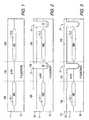
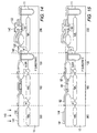
- Figures 1-19 show sequential process steps in the formation of a TCRL in a BiCMOS process.
- Figures 20-25 show experimental results for the TCRL.
- Figure 26 shows a more-detailed cross-section of the NPN bipolar device formed in the invention's BiCMOS process.
- a P-type substrate has its upper surface covered with a suitable ion implantation mask such as deposited oxide, thermally-grown oxide or photoresist. Openings are made in the resist mask to define the N+ buried layer regions 12.1 and 12.2. Those regions are implanted with a first N-type dopant such as Arsenic. The implantation mask is then stripped.
- a suitable ion implantation mask such as deposited oxide, thermally-grown oxide or photoresist. Openings are made in the resist mask to define the N+ buried layer regions 12.1 and 12.2. Those regions are implanted with a first N-type dopant such as Arsenic. The implantation mask is then stripped.
- the substrate is then covered with a second suitable ion implantation mask such as deposited oxide, thermally-grown oxide or photoresist. Openings are made in the mask to define other buried layer regions, into which are implanted a second N-type dopant with a significantly different diffusion coefficient than the first.
- a second suitable ion implantation mask such as deposited oxide, thermally-grown oxide or photoresist. Openings are made in the mask to define other buried layer regions, into which are implanted a second N-type dopant with a significantly different diffusion coefficient than the first.
- the two different buried layer dopants enable the fabricating of transistors with varying collector profiles, which can be tailored to address speed versus breakdown voltage tradeoffs in the RF devices.
- Two different collector profiles, coupled with the use of the selectively implanted collector provide for an integrated circuit with four NPN devices.
- N+ buried layers 12.1 and 12.2 are driven in with a suitable annealing operation and an N-type epitaxial layer 11 is grown on top of the substrate 10.
- the substrate 10 is patterned into CMOS regions 100 that are separated from bipolar NPN regions 200 by transition regions 150.
- the N-type buried layers 12.1 and 12.2 are formed beneath regions that will receive P-type wells. No buried layer is required for the N-type wells.
- the initial trench formation step is shown in Figure 2. Isolation trenches are formed between transition region 150 and the NPN transistor region as well as in other locations as needed for improved lateral isolation.
- a trench photoresist mask 20 is uniformly deposited and patterned on the substrate 10. The photoresist is developed to expose the trench regions 21.
- a suitable wet or dry etch operation etches the trenches 21 down to a level below the N+ buried layers 12.1 and 12.2. The bottoms of the trenches are then implanted with a suitable P+ channel stop 22.
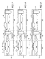
- the next step includes stripping the photoresist 20, performing thermal oxidation on the trench sidewalls and depositing and patterning a sidewall dielectric layer 23 such as an oxide nitride sandwich.
- Oxidation layer 23 is densified, providing a polish stop for planarization.
- Nitride in this layer has the feature of closely matching the thermal characteristics of silicon.
- the layer is formed at a thickness which is thin enough to prevent any overhang of the trench cavity, thereby allowing complete trench fill during subsequent deposition steps.
- Oxidation layer 23 also provides a pad oxide for LOCOS at a later stage. The combination of thermal oxidation, oxide deposition and oxide densification allows the trench sidewall to match the thermal expansion rate of the silicon substrate.
- An alternate embodiment would be to deposit the sidewall dielectric layer in such a way that would cause subsequent trench fill to form a void in the trench which is below the surface of the silicon substrate. This feature provides stress relief and eliminates silicon defect generation in the silicon adjacent the trench.
- the substrate 10 is then subjected to a polysilicon deposition step that deposits a polysilicon layer 24 over the substrate 10 and epitaxial layer 11 and fills the trenches 21.
- the undoped polysilicon fill is a semi-insulating material, which provides a favorable electrical characteristic for RF parasitic capacitances.
- Figure 4 shows completion of the trenches.
- the substrate 10 and epitaxial layer 11 are planarized to remove the layers of polysilicon 24 and the thermal oxide 23 from the surface of the substrate 10 and epitaxial layer 11 in all areas except above the trenches.
- Such planarization is accomplished with a conventional chemical mechanical polishing operation.
- the nitride underneath the polysilicon serves as a hard stop during the polish operation and protects the underlying oxide and silicon from damage.
- the thinness of the oxide nitride sandwich also assures the precise match of the polished trench polysilicon surface to the original silicon surface.
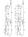
- the trenches are initially protected from the subsequent CMOS processing steps.
- This protection includes forming a pad oxide layer 51 over the trenches.
- Pad oxide layer 51 is followed by an N+ sinker photoresist deposition, patterning, and implantation step to form the N+ sinker 52 for the future collector of the NPN transistors 200.
- a layer of silicon nitride 54 is deposited over the pad oxide 51 on the surface of the substrate 10 and epitaxial layer 11.
- the silicon nitride is initially patterned to expose local oxidation (LOCOS) regions 50. Following LOCOS patterning, a conventional LOCOS operation fabricates LOCOS regions 50 that provide surface lateral isolation of the NMOS and PMOS devices 100 and separate the sinker diffusion 52 from the rest of the NPN transistor 200. The silicon nitride is stripped from the rest of the surface of the substrate 10 and epitaxial layer 11 except for regions above the trenches 21.
- LOCOS local oxidation
- a 'skin' layer of silicon dioxide forms on the surface of the nitride oxidation mask.
- This skin layer is patterned using conventional photoresist and wet etch, leaving the skin layer over the trench regions. After photoresist removal, the nitride is removed in a suitable wet etch chemistry except for regions above the trenches 21.
- This oxide layer allows simultaneous protection of the trench areas and removal of the nitride in a manner completely benign to the underlying pad ox and silicon substrate regions. Protection of these regions from further stress-generating thermal oxidation is important to the successful fabrication of shallow transistor structures, which follows as taught in U.S. Patent #5,892,264.
- the pad oxide is then removed from the surface of substrate 10 and epitaxial layer 11 to expose the surface for further fabrication.
- a sacrificial oxidation is performed on the surface of epitaxial layer 11.
- the oxidation is a typical first step in the formation of N-wells and P-wells for the CMOS devices 100.
- Suitable photoresist masks and implants 62 provide the N-wells and P-wells for the CMOS devices.
- a heavier P-type implant 64 provides junction isolation to separate PMOS and NMOS devices.
- a gate oxide layer 65 typically a thermal oxide, is grown on the surface of epitaxial layer 11. That step is followed by uniform, deposition of a layer of polysilicon which is subsequently patterned and doped to form polysilicon gates 66.
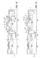
- the NMOS and PMOS drains receive a typical lightly-doped drain implant 72 (N) or (P) respectively (the P-type implant is not shown here) for forming the N-type lightly-doped drain regions and the P-type lightly-doped drain regions.
- An annealing step drives the lightly doped drains slightly under the sidewall of the gates.
- the lightly doped drain regions use the sidewalls of the gate as masks. These regions are self-aligned in a conventional manner using the gate as masks followed by suitable P-type and N-type implants.
- a typical P+ resistor is formed in the N-type epitaxial region 11 using a suitable photoresist and implant.
- an NPN protection spacer oxide layer 78 is uniformly deposited over epitaxial layer 11.
- the spacer oxide 78 covers the transition region 150 and NPN region 200 of layer 11, Without this spacer oxide coverage, subsequent CMOS processing steps would interfere with the formation of the NPN transistor.
- the spacer oxide layer over the gate 66 is patterned and removed to leave sidewall spacers 70.1, 70.2 at the edges of the gate 66.
- the spacer oxide layer 78 not only provides the sidewall spacers for the CMOS devices but also provides a hard mask and surface isolation for the active elements of the NPN transistor. Performing this deposition step early in the process saves one or more deposition and masking steps later in the process. As a result, the spacer oxide layer 78 forms the mask for the self aligned sources and drains of the CMOS devices and the mask for the collector and emitter openings 126, 127, respectively. See Figure 12 for these later process effects.
- CMOS processing step is shown in Figure 8.
- a screen oxide layer 80 is deposited and patterned to cover the lightly doped source and drain regions of the CMOS device. Those regions are then suitably implanted with either P+ or N+ ions to form sources 81 and drains 82. The respective P-type and N-type sources and drains are then subjected to an annealing operation where the diffusion time is set to adjust the depth of the sources and drains. While the figures show only one MOS device, those skilled in the art understand that the process disclosed herein can be used to form multiple transistors including pluralities of NMOS, PMOS and bipolar devices.
- CMOS nitride etch stop protection layer 90 As shown in Figure 9, is uniformly deposited over epitaxial layer 11. On top of the nitride protection layer, there is deposited a CMOS oxide protection layer 92. Since the two protection layers can be selectively etched with respect to each other, the combination of deposited layers in two sequential steps saves a substantial number of future process steps by using the two layers as different etch stops.
- a photoresist layer 94 is deposited and patterned to cover the CMOS devices and at least part of the LOCOS region that extends from the transition region 150 into the CMOS region 100.
- the CMOS oxide protection layer 92 and nitride protection layer 90 are stripped from the exposed NPN region 200 using suitable wet etchings. As a result of sequential etching operations, the spacer oxide layer 78 is exposed as shown in Figure 10.
- a thermal oxide photoresist layer 110 is uniformly deposited over spacer oxide layer 78 and patterned to have openings 112 and 114 in the NPN section 200. With the photoresist 110 in place, the spacer oxide in exposed regions 112 and 114 is removed in order to expose the surface of the sinker diffusion 52 and the surface of the subsequent NPN transistor 200.
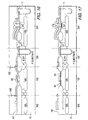
- the extrinsic base comprises a stack of layers that are deposited on the epitaxial layer 11.
- these layers include a doped polysilicon layer 120, a tungsten silicide layer 121, a polysilicon cap layer 122, an inter-poly oxide layer 123 and a titanium nitride anti-reflective coating 124.
- the polysilicon layer 120, WSi layer 121 and polysilicon cap layer 122 are deposited followed by an implant of boron that will form the doping for the extrinsic base 222.
- the polysilicon cap layer is included to prevent the boron doping from segregating heavily at the top of the poly/ WSi layer and not adequately diffusing into the silicon to create the extrinsic base. It also prevents unwanted sputtering of the WSi layer during the boron implant, which could potentially contaminate the implant tool with heavy metallics.
- the stack is suitably patterned to form the emitter opening 127.
- dopants from layer 120 form the extrinsic base 222.
- a further boron implant through the emitter opening forms the intrinsic base 220.
- a SIC (Selectively Implanted Collector) implant 224 is also made through the intrinsic base 220 and the emitter hole 127.
- the stack pattern mask helps mask the high energy SIC implant and creates a perfect self-alignment of the SIC to the transistor.
- the SIC implant 224 contacts the N+ buried layer 12.2.
- the SIC implant 224 is annealed, the emitter surface is oxidized and a P-type implant completes the intrinsic base 220.
- a layer of base spacer oxide 130 is deposited to mask the base region.
- a nitride spacer layer 131 is deposited and etched to open the emitter region.
- the base spacer oxide is etched with suitable hydrofluoric acid.
- the structure of the composite spacer allows the emitter-to-extrinsic-base spacing, and hence, speed-versus-breakdown device tradeoffs, to be varied easily by changing the nitride spacer deposition thickness, the base spacer oxide etch time, or both.
- an emitter polysilicon layer 132 is deposited and patterned to form the emitter contact 134 and the collector contact 133.
- the N-type dopants from the emitter poly layer 132 diffuse into the surface of the epitaxial layer 11 in order to form the collector surface contact and the emitter of the NPN transistors 200.
- FIGs 14 and 15 show the formation of the polysilicon resistor with a relatively low temperature coefficient of resistance (TCRL) resistor 141.
- TCRL temperature coefficient of resistance
- a protective oxide 140 is deposited over the emitter polysilicon layer 132. This layer protects any exposed emitter polysilicon layer 132 from etching when the TCRL regions are defined.
- a polysilicon layer 142 is deposited in the opening.
- the polysilicon layer is implanted with a BF 2 implant 143.
- the TCRL 141 is covered with a photoresist and etched to its suitable size.
- the TCRL layer 141 is then covered with a protective oxide 144.
- the oxide is suitably patterned and masked to protect the underlying portion of the TCRL 141, while uncovering the contact regions of the resistor.
- the TCRL poly layer is deposited late in the process. As such, it is possible to deposit an amorphous silicon film and then adjust its resistivity by adding dopants.
- This process of the invention forms a TCRL resistor 141 that has a resistance of 750 ohms per square and a temperature coefficient of resistance that is less than 100 parts per million (ppm).
- the resistor is formed using a non-selective BF 2 implant to dope the polysilicon layer.
- a 900°C rapid thermal annealing (RTA) step activates the resistor implant and sets the final doping profiles for the bipolar and MOS devices 200, 100.
- RTA rapid thermal annealing
- a TCRL poly layer is deposited late in the process.
- the invention's process deposits an amorphous silicon film and then adjusts its resistivity by adding dopants.
- a non-selective BF 2 implant is used to dope the film.
- a mask is used to clear oxide from all contact areas and a 900°C RTA step activates resistor implants to set the final doping. Resistor contacts are i consequently silicided before final back end processing.
- the TCRL resistor 141 separates the resistance from temperature sensitivity.
- high resistivity resulted in a greater temperature sensitivity.
- Antecedents to the inventive process attempted to separate those two characteristics by providing a relatively thin film with dopings adjusted to set the resistivity to 750 ohms per square.
- dopings adjusted to set the resistivity to 750 ohms per square.
- BF 2 implants approach a high level, an unanticipated and counter-intuitive increase in resistance was observed. This behavior was not observed when only boron was used to dope this film. Normal expectations were that higher implant levels would decrease resistance, not increase it.
- the polysilicon layer 142 has a thickness of 70nm and may be in a range of from 65nm to 75nm.
- the implant concentration of boron ions 142 is 1.3 x 10 16 and may be in a range from 9 x 10 15 to 1.5 x 10 16 .
- Yamaguchi, et al. [Yamaguchi, et al., " Process and Device Characterization for a 30-GHz ft Submicrometer Double Poly-Si Bipolar Technology Using BF2-Implanted Base with Rapid Thermal Process", IEEE TED, August 1993.] observed the same relationship between TCR and sheet resistance.
- TCRs of boron-doped P-type polysilicon resistors fabricated with a 150nm amorphous layer approach zero at sheet resistances of 600-800 ohms per square.
- resistance declines with increasing boron doses.
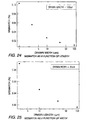
- Table 2 shows the effects of RTA temperature on sheet resistance and TCR as a function of implant dose.
- Figure 21 is a scatter plot of a 30 x 30 micron resistor showing the relationship of TCR to sheet resistance at 50°C was chosen as the lowest measurement point.
- the TCR is calculated by fitting a line to values measured from 50-125°C at 25° intervals.
- the dashed lines denote the objectives that were set for this development project.
- Figure 22 shows average changes in sheet resistance for nine parts measured over this temperature range while Figure 23 is a plot of the calculated TCRs for this set of measurements.
- the solid line represents a linear fit while the dashed line is a polynomial fit.
- the upward "hook" observed at lower temperature is typical to that of diffused resistors.
- Figure 24 shows the percent mismatch as a function of length for a fixed width resistor and Figure 25 represents the same parameter as a function of width with a fixed length.
- the data, as expected, show improved matching with increasing dimensions.
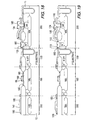
- the TCRL resistor 141 and the NPN transistor regions 200 are protected with a layer of photoresist 160.
- the photoresist is patterned to open a region above the CMOS devices 100.
- the protective oxide 92 (Fig. 15) is removed.
- the photoresist layer 160 is removed, followed by removal of the nitride protect layer 90.
- the emitter 170 and the resistor 141 are subjected to an RTA step.
- the step is carried out at approximately 900°C for 0.5 minutes, and completes the fabrication of the emitter first prepared in the steps shown previously in Figure 13.
- the screen oxide layer 80 over the lightly doped source and drain regions of the CMOS device is then removed.
- the exposed polysilicon regions of the resistor 141, the gate 66, the source and drain regions, and the collector and emitter contacts 133, 134 are silicided with platinum 180 to form a platinum silicide layer on the exposed polysilicon.
- a sidewall spacer oxide 190 is applied to the sidewalls of the emitter contact 134 and the collector contact 133.
- the substrate is subjected to suitable metallization layers, including the formation of three metal layers separated from each other by suitable insulating layers and separate layers being selectively interconnected, one to the other, by the formation of vias that are filled with conductive material.
- suitable metallization layers including the formation of three metal layers separated from each other by suitable insulating layers and separate layers being selectively interconnected, one to the other, by the formation of vias that are filled with conductive material.
- a passivation layer typically silicon nitride
- a substrate including the integrated circuits and devices made thereon are then further processed for testing and assembly.
- a low temperature coefficient resistor has some unrepaired ion implant damage. The damaged portion raises the resistance and renders the resistor less sensitive to operating temperature fluctuations.
- a polysilicon thin film low temperature coefficient resistor and a method for the resistor's fabrication overcomes the coefficient of resistance problem of the prior art, while at the same time eliminating steps from the BiCMOS fabrication process, optimizing bipolar design tradeoffs, and improving passive device isolation.
- a low temperature coefficient of resistance resistor (TCRL) is formed on a layer of insulation, typically silicon dioxide or silicon nitride, the layer comprising polysilicon having a relatively high concentration of dopants of one or more species.
- An annealing process is used for the implanted resistor which is shorter than that for typical prior art implanted resistors, leaving some intentional unannealed damage in the resistor.
- the planned damage gives the TCRL a higher resistance without increasing its temperature coefficient.
- a process for fabrication of the resistor is used which combines separate spacer oxide depositions, provides buried layers having different diffusion coefficients, incorporates dual dielectric trench sidewalls that double as a polish stop, supplies a spacer structure that controls precisely the emitter-base dimension, and integrates bipolar and CMOS devices with negligible compromise to the features of either type.
Landscapes
- Engineering & Computer Science (AREA)
- Power Engineering (AREA)
- Computer Hardware Design (AREA)
- Microelectronics & Electronic Packaging (AREA)
- General Physics & Mathematics (AREA)
- Physics & Mathematics (AREA)
- Condensed Matter Physics & Semiconductors (AREA)
- Manufacturing & Machinery (AREA)
- Chemical & Material Sciences (AREA)
- Crystallography & Structural Chemistry (AREA)
- Metal-Oxide And Bipolar Metal-Oxide Semiconductor Integrated Circuits (AREA)
- Bipolar Transistors (AREA)
- Semiconductor Integrated Circuits (AREA)
- Bipolar Integrated Circuits (AREA)
- Non-Adjustable Resistors (AREA)
- Internal Circuitry In Semiconductor Integrated Circuit Devices (AREA)
Applications Claiming Priority (2)
| Application Number | Priority Date | Filing Date | Title |
|---|---|---|---|
| US09/345,929 US6351021B1 (en) | 1999-07-01 | 1999-07-01 | Low temperature coefficient resistor (TCRL) |
| US345929 | 2000-06-29 |
Publications (2)
| Publication Number | Publication Date |
|---|---|
| EP1065715A2 true EP1065715A2 (fr) | 2001-01-03 |
| EP1065715A3 EP1065715A3 (fr) | 2005-01-05 |
Family
ID=23357144
Family Applications (2)
| Application Number | Title | Priority Date | Filing Date |
|---|---|---|---|
| EP00401828A Withdrawn EP1065704A3 (fr) | 1999-07-01 | 2000-06-27 | Resistance à faible coefficient de température |
| EP00401889A Withdrawn EP1065715A3 (fr) | 1999-07-01 | 2000-06-30 | Procédé BiCMOS avec résisteur à faible coefficient de température |
Family Applications Before (1)
| Application Number | Title | Priority Date | Filing Date |
|---|---|---|---|
| EP00401828A Withdrawn EP1065704A3 (fr) | 1999-07-01 | 2000-06-27 | Resistance à faible coefficient de température |
Country Status (5)
| Country | Link |
|---|---|
| US (1) | US6351021B1 (fr) |
| EP (2) | EP1065704A3 (fr) |
| JP (1) | JP2001057410A (fr) |
| KR (2) | KR20010015135A (fr) |
| TW (2) | TW465073B (fr) |
Cited By (1)
| Publication number | Priority date | Publication date | Assignee | Title |
|---|---|---|---|---|
| US6936529B2 (en) | 2003-06-30 | 2005-08-30 | Hynix Semiconductor Inc. | Method for fabricating gate-electrode of semiconductor device with use of hard mask |
Families Citing this family (7)
| Publication number | Priority date | Publication date | Assignee | Title |
|---|---|---|---|---|
| SE0103036D0 (sv) | 2001-05-04 | 2001-09-13 | Ericsson Telefon Ab L M | Semiconductor process and integrated circuit |
| DE10322588B4 (de) * | 2003-05-20 | 2006-10-05 | Infineon Technologies Ag | Verfahren zum Herstellen einer Widerstandsschicht |
| US7285472B2 (en) * | 2005-01-27 | 2007-10-23 | International Business Machines Corporation | Low tolerance polysilicon resistor for low temperature silicide processing |
| US7241663B2 (en) * | 2005-04-19 | 2007-07-10 | Texas Instruments Incorporated | Maskless multiple sheet polysilicon resistor |
| CN102074474B (zh) * | 2009-11-24 | 2013-07-10 | 无锡华润上华半导体有限公司 | 双极晶体管的制造方法 |
| CN103151312B (zh) * | 2011-12-07 | 2014-12-10 | 上海华虹宏力半导体制造有限公司 | 一种在cmos源漏注入前进行多晶硅掺杂的方法 |
| US9761581B1 (en) | 2016-03-03 | 2017-09-12 | Texas Instruments Incorporated | Single mask level including a resistor and a through-gate implant |
Citations (6)
| Publication number | Priority date | Publication date | Assignee | Title |
|---|---|---|---|---|
| JPS58106855A (ja) * | 1981-12-18 | 1983-06-25 | Fujitsu Ltd | 半導体装置の製造方法 |
| US4467519A (en) * | 1982-04-01 | 1984-08-28 | International Business Machines Corporation | Process for fabricating polycrystalline silicon film resistors |
| JPS60116160A (ja) * | 1983-11-29 | 1985-06-22 | Sony Corp | 半導体装置の製造方法 |
| US4579600A (en) * | 1983-06-17 | 1986-04-01 | Texas Instruments Incorporated | Method of making zero temperature coefficient of resistance resistors |
| US5240511A (en) * | 1987-02-20 | 1993-08-31 | National Semiconductor Corporation | Lightly doped polycrystalline silicon resistor having a non-negative temperature coefficient |
| US5489547A (en) * | 1994-05-23 | 1996-02-06 | Texas Instruments Incorporated | Method of fabricating semiconductor device having polysilicon resistor with low temperature coefficient |
Family Cites Families (2)
| Publication number | Priority date | Publication date | Assignee | Title |
|---|---|---|---|---|
| FR2681978B1 (fr) * | 1991-09-26 | 1993-12-24 | Sgs Thomson Microelectronics Sa | Resistance de precision et procede de fabrication. |
| KR100292851B1 (ko) | 1991-09-27 | 2001-09-17 | 스콧 티. 마이쿠엔 | 높은얼리전압,고주파성능및고항복전압특성을구비한상보형바이폴라트랜지스터및그제조방법 |
-
1999
- 1999-07-01 US US09/345,929 patent/US6351021B1/en not_active Expired - Lifetime
-
2000
- 2000-06-12 TW TW089111416A patent/TW465073B/zh not_active IP Right Cessation
- 2000-06-27 EP EP00401828A patent/EP1065704A3/fr not_active Withdrawn
- 2000-06-30 JP JP2000199797A patent/JP2001057410A/ja active Pending
- 2000-06-30 EP EP00401889A patent/EP1065715A3/fr not_active Withdrawn
- 2000-07-01 KR KR1020000037587A patent/KR20010015135A/ko not_active Application Discontinuation
- 2000-07-01 KR KR1020000037588A patent/KR20010015136A/ko not_active Application Discontinuation
- 2000-07-28 TW TW089113089A patent/TW495921B/zh not_active IP Right Cessation
Patent Citations (6)
| Publication number | Priority date | Publication date | Assignee | Title |
|---|---|---|---|---|
| JPS58106855A (ja) * | 1981-12-18 | 1983-06-25 | Fujitsu Ltd | 半導体装置の製造方法 |
| US4467519A (en) * | 1982-04-01 | 1984-08-28 | International Business Machines Corporation | Process for fabricating polycrystalline silicon film resistors |
| US4579600A (en) * | 1983-06-17 | 1986-04-01 | Texas Instruments Incorporated | Method of making zero temperature coefficient of resistance resistors |
| JPS60116160A (ja) * | 1983-11-29 | 1985-06-22 | Sony Corp | 半導体装置の製造方法 |
| US5240511A (en) * | 1987-02-20 | 1993-08-31 | National Semiconductor Corporation | Lightly doped polycrystalline silicon resistor having a non-negative temperature coefficient |
| US5489547A (en) * | 1994-05-23 | 1996-02-06 | Texas Instruments Incorporated | Method of fabricating semiconductor device having polysilicon resistor with low temperature coefficient |
Non-Patent Citations (2)
| Title |
|---|
| PATENT ABSTRACTS OF JAPAN vol. 0072, no. 14 (E-199), 21 September 1983 (1983-09-21) & JP 58 106855 A (FUJITSU KK), 25 June 1983 (1983-06-25) * |
| PATENT ABSTRACTS OF JAPAN vol. 0092, no. 70 (E-353), 26 October 1985 (1985-10-26) & JP 60 116160 A (SONY KK), 22 June 1985 (1985-06-22) * |
Cited By (1)
| Publication number | Priority date | Publication date | Assignee | Title |
|---|---|---|---|---|
| US6936529B2 (en) | 2003-06-30 | 2005-08-30 | Hynix Semiconductor Inc. | Method for fabricating gate-electrode of semiconductor device with use of hard mask |
Also Published As
| Publication number | Publication date |
|---|---|
| JP2001057410A (ja) | 2001-02-27 |
| EP1065715A3 (fr) | 2005-01-05 |
| KR20010015135A (ko) | 2001-02-26 |
| TW495921B (en) | 2002-07-21 |
| KR20010015136A (ko) | 2001-02-26 |
| EP1065704A2 (fr) | 2001-01-03 |
| EP1065704A3 (fr) | 2005-01-12 |
| US6351021B1 (en) | 2002-02-26 |
| TW465073B (en) | 2001-11-21 |
Similar Documents
| Publication | Publication Date | Title |
|---|---|---|
| KR100918716B1 (ko) | 반도체 공정 및 집적회로 | |
| US5219784A (en) | Spacer formation in a bicmos device | |
| US5880502A (en) | Low and high voltage CMOS devices and process for fabricating same | |
| KR100691036B1 (ko) | 횡형 바이폴라 트랜지스터를 구비하는 집적 회로 및 그 제조 방법 | |
| JPH04226066A (ja) | Bicmos装置及びその製造方法 | |
| US6670228B2 (en) | Method of fabricating a polysilicon capacitor utilizing FET and bipolar base polysilicon layers | |
| EP1273036B1 (fr) | Procede de fabrication d'un circuit integre a heterojonction bicmos | |
| EP0418670B1 (fr) | Procédé pour la fabrication de circuits BiMOS de haute performance | |
| EP0768709A2 (fr) | Procédé BiCMOS avec transistor bipolaire ayant un faible courant de recombinaison de base | |
| JPH04226064A (ja) | 半導体装置用の相互接続体及びその製造方法 | |
| US6812108B2 (en) | BICMOS process with low temperature coefficient resistor (TCRL) | |
| US6767797B2 (en) | Method of fabricating complementary self-aligned bipolar transistors | |
| EP1065715A2 (fr) | Procédé BiCMOS avec résisteur à faible coefficient de température | |
| EP1214737B1 (fr) | Procede de production d'une diode a capacite variable de schottky | |
| US6798024B1 (en) | BiCMOS process with low temperature coefficient resistor (TCRL) | |
| US5998843A (en) | Semiconductor device with stable threshold voltages | |
| US20040209433A1 (en) | Method for manufacturing and structure of semiconductor device with shallow trench collector contact region | |
| US11984362B1 (en) | Control of locos structure thickness without a mask | |
| KR20020006583A (ko) | 저온 계수 저항기를 갖는 개선된 비씨모스 공정 | |
| JPH04255231A (ja) | バイポーラトランジスタの製造方法 | |
| SE522527C2 (sv) | Halvledarprocess och integrerad krets | |
| JPH077096A (ja) | 完全封入式セルフアライン分離工程 |
Legal Events
| Date | Code | Title | Description |
|---|---|---|---|
| PUAI | Public reference made under article 153(3) epc to a published international application that has entered the european phase |
Free format text: ORIGINAL CODE: 0009012 |
|
| AK | Designated contracting states |
Kind code of ref document: A2 Designated state(s): AT BE CH CY DE DK ES FI FR GB GR IE IT LI LU MC NL PT SE |
|
| AX | Request for extension of the european patent |
Free format text: AL;LT;LV;MK;RO;SI |
|
| RIC1 | Information provided on ipc code assigned before grant |
Ipc: 7H 01L 21/8249 B Ipc: 7H 01L 27/06 B Ipc: 7H 01L 27/02 B Ipc: 7H 01L 27/08 B Ipc: 7H 01L 21/02 A |
|
| PUAL | Search report despatched |
Free format text: ORIGINAL CODE: 0009013 |
|
| AK | Designated contracting states |
Kind code of ref document: A3 Designated state(s): AT BE CH CY DE DK ES FI FR GB GR IE IT LI LU MC NL PT SE |
|
| AX | Request for extension of the european patent |
Extension state: AL LT LV MK RO SI |
|
| STAA | Information on the status of an ep patent application or granted ep patent |
Free format text: STATUS: THE APPLICATION IS DEEMED TO BE WITHDRAWN |
|
| 18D | Application deemed to be withdrawn |
Effective date: 20050104 |