Advanced wireless communications products demand integrated circuit technologies
with high performance, high levels of system integration, low power and low cost. For
wireless applications up to several GHz, silicon BiCMOS technology is uniquely suited to
meet these requirements. Of critical important to RF design is the availability of high quality
passive components. In particular, it is desirable to have implanted thin film resistors that
have a low temperature coefficient of resistance. Unfortunately, existing techniques for
polysilicon thin film resistors generally result in thin film resistors with relatively large
temperature coefficients of resistance.
The invention comprises a polysilicon thin film low temperature coefficient resistor
and a method for the resistor's fabrication that overcome the coefficient of resistance problem
of the prior art, while at the same time eliminating steps from the BiCMOS fabrication
process, optimizing bipolar design tradeoffs, and improving passive device isolation. The
low temperature coefficient of resistance resistor (TCRL) is formed on a layer of insulation,
typically silicon dioxide or silicon nitride. The layer comprises polysilicon that has a
relatively high concentration of dopants of one or more species, and has a substantial amount
of unannealed implant damage. Contrary to prior art methods, the implanted resistor is
annealed less than typical prior art implanted resistors in order to leave some planned
unannealed damage in the resistor. The planned damage gives the TCRL a higher resistance
without increasing its temperature coefficient. Thus, even though the temperature may
increase, the relative value of the resistance remains the same. As such, the resistor is more
precise than others produced with current methods, and may be used where precision
requirements for high quality RF devices apply. A process for fabrication of the resistor is
used which combines separate spacer oxide depositions, provides buried layers having
different diffusion coefficients, incorporates dual dielectric trench sidewalls that double as
a polish stop, supplies a spacer structure that controls precisely the emitter-base dimension,
and integrates bipolar and CMOS devices with negligible compromise to the features of either
type.
In order to highlight features of the invention by way of example, while showing them
in their proper context, the proportions shown in the figures are not to scale.
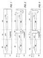
Figures 1-19 show sequential process steps in the formation of a TCRL in a BiCMOS
process.
Figures 20-25 show experimental results for the TCRL.
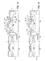
Figure 26 shows a more-detailed cross-section of the NPN bipolar device formed in
the invention's BiCMOS process.
All figures show the lateral division of the regions of the substrate into CMOS regions
100, bipolar NPN regions 200, and transition regions 150 between the CMOS and bipolar
regions. The regional divisions are shown by dotted lines.
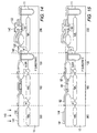
Refer first to Figure 1. A P-type substrate has its upper surface covered with a suitable
ion implantation mask such as deposited oxide, thermally-grown oxide or photoresist.
Openings are made in the resist mask to define the N+ buried layer regions 12.1 and 12.2.
Those regions are implanted with a first N-type dopant such as Arsenic. The implantation
mask is then stripped.
The substrate is then covered with a second suitable ion implantation mask such as
deposited oxide, thermally-grown oxide or photoresist. Openings are made in the mask to
define other buried layer regions, into which are implanted a second N-type dopant with a
significantly different diffusion coefficient than the first. The two different buried layer
dopants enable the fabricating of transistors with varying collector profiles, which can be
tailored to address speed versus breakdown voltage tradeoffs in the RF devices. Two
different collector profiles, coupled with the use of the selectively implanted collector,
provide for an integrated circuit with four NPN devices.
N+ buried layers 12.1 and 12.2 are driven in with a suitable annealing operation and
an N-type epitaxial layer 11 is grown on top of the substrate 10. As a result, the substrate 10
is patterned into CMOS regions 100 that are separated from bipolar NPN regions 200 by
transition regions 150. The N-type buried layers 12.1 and 12.2 are formed beneath regions
that will receive P-type wells. No buried layer is required for the N-type wells.
The initial trench formation step is shown in Figure 2. Isolation trenches are formed
between transition region 150 and the NPN transistor region as well as in other locations as
needed for improved lateral isolation. A trench photoresist mask 20 is uniformly deposited
and patterned on the substrate 10. The photoresist is developed to expose the trench regions
21. A suitable wet or dry etch operation etches the trenches 21 down to a level below the N+
buried layers 12.1 and 12.2. The bottoms of the trenches are then implanted with a suitable
P+ channel stop 22.
As shown in Figure 3, the next step includes stripping the photoresist 20, performing
thermal oxidation on the trench sidewalls and depositing and patterning a sidewall dielectric
layer 23 such as an oxide nitride sandwich. Oxidation layer 23 is densified, providing a polish
stop for planarization. Nitride in this layer has the feature of closely matching the thermal
characteristics of silicon. The layer is formed at a thickness which is thin enough to prevent
any overhang of the trench cavity, thereby allowing complete trench fill during subsequent
deposition steps. Oxidation layer 23 also provides a pad oxide for LOCOS at a later stage.
The combination of thermal oxidation, oxide deposition and oxide densification allows the
trench sidewall to match the thermal expansion rate of the silicon substrate.
An alternate embodiment would be to deposit the sidewall dielectric layer in such a
way that would cause subsequent trench fill to form a void in the trench which is below the
surface of the silicon substrate. This feature provides stress relief and eliminates silicon defect
generation in the silicon adjacent the trench.
The substrate 10 is then subjected to a polysilicon deposition step that deposits a
polysilicon layer 24 over the substrate 10 and epitaxial layer 11 and fills the trenches 21. The
undoped polysilicon fill is a semi-insulating material, which provides a favorable electrical
characteristic for RF parasitic capacitances.
Figure 4 shows completion of the trenches. The substrate 10 and epitaxial layer 11 are
planarized to remove the layers of polysilicon 24 and the thermal oxide 23 from the surface
of the substrate 10 and epitaxial layer 11 in all areas except above the trenches. Such
planarization is accomplished with a conventional chemical mechanical polishing operation.
The nitride underneath the polysilicon serves as a hard stop during the polish operation and
protects the underlying oxide and silicon from damage. The thinness of the oxide nitride
sandwich also assures the precise match of the polished trench polysilicon surface to the
original silicon surface.
It is important both to protect the trenches 21 and to cover the NPN region 200 during
formation of the CMOS devices. Likewise, it is a goal of this process to combine as many of
the CMOS and bipolar processing steps as possible. Accordingly, turning to Figure 5, the
trenches are initially protected from the subsequent CMOS processing steps. This protection
includes forming a pad oxide layer 51 over the trenches. Pad oxide layer 51 is followed by
an N+ sinker photoresist deposition, patterning, and implantation step to form the N+ sinker
52 for the future collector of the NPN transistors 200. Next, a layer of silicon nitride 54 is
deposited over the pad oxide 51 on the surface of the substrate 10 and epitaxial layer 11. The
silicon nitride is initially patterned to expose local oxidation (LOCOS) regions 50. Following
LOCOS patterning, a conventional LOCOS operation fabricates LOCOS regions 50 that
provide surface lateral isolation of the NMOS and PMOS devices 100 and separate the sinker
diffusion 52 from the rest of the NPN transistor 200. The silicon nitride is stripped from the
rest of the surface of the substrate 10 and epitaxial layer 11 except for regions above the
trenches 21.
During the LOCOS operation, a 'skin' layer of silicon dioxide forms on the surface of
the nitride oxidation mask. This skin layer is patterned using conventional photoresist and
wet etch, leaving the skin layer over the trench regions. After photoresist removal, the nitride
is removed in a suitable wet etch chemistry except for regions above the trenches 21. The use
of this oxide layer allows simultaneous protection of the trench areas and removal of the
nitride in a manner completely benign to the underlying pad ox and silicon substrate regions.
Protection of these regions from further stress-generating thermal oxidation is important to
the successful fabrication of shallow transistor structures, which follows as taught in U.S.
Patent #5,892,264.
The pad oxide is then removed from the surface of substrate 10 and epitaxial layer 11
to expose the surface for further fabrication.
Refer now to Figure 6. In the next step, a sacrificial oxidation is performed on the
surface of epitaxial layer 11. The oxidation is a typical first step in the formation of N-wells
and P-wells for the CMOS devices 100. Suitable photoresist masks and implants 62 provide
the N-wells and P-wells for the CMOS devices. A heavier P-type implant 64 provides
junction isolation to separate PMOS and NMOS devices. Following removal of the sacrificial
oxide, a gate oxide layer 65, typically a thermal oxide, is grown on the surface of epitaxial
layer 11. That step is followed by uniform, deposition of a layer of polysilicon which is
subsequently patterned and doped to form polysilicon gates 66.
The next stage in the fabrication of the CMOS transistors is shown in Figure 7. Next,
the NMOS and PMOS drains receive a typical lightly-doped drain implant 72 (N) or (P)
respectively (the P-type implant is not shown here) for forming the N-type lightly-doped
drain regions and the P-type lightly-doped drain regions. An annealing step drives the
lightly doped drains slightly under the sidewall of the gates. The lightly doped drain regions
use the sidewalls of the gate as masks. These regions are self-aligned in a conventional
manner using the gate as masks followed by suitable P-type and N-type implants. Following
that step, in a region not shown in the figure, a typical P+ resistor is formed in the N-type
epitaxial region 11 using a suitable photoresist and implant. Next, an NPN protection spacer
oxide layer 78 is uniformly deposited over epitaxial layer 11. The spacer oxide 78 covers the
transition region 150 and NPN region 200 of layer 11, Without this spacer oxide coverage,
subsequent CMOS processing steps would interfere with the formation of the NPN transistor.
The spacer oxide layer over the gate 66 is patterned and removed to leave sidewall spacers
70.1, 70.2 at the edges of the gate 66.
The spacer oxide layer 78 not only provides the sidewall spacers for the CMOS devices
but also provides a hard mask and surface isolation for the active elements of the NPN
transistor. Performing this deposition step early in the process saves one or more deposition
and masking steps later in the process. As a result, the spacer oxide layer 78 forms the mask
for the self aligned sources and drains of the CMOS devices and the mask for the collector
and emitter openings 126, 127, respectively. See Figure 12 for these later process effects.
The next CMOS processing step is shown in Figure 8. A screen oxide layer 80 is
deposited and patterned to cover the lightly doped source and drain regions of the CMOS
device. Those regions are then suitably implanted with either P+ or N+ ions to form sources
81 and drains 82. The respective P-type and N-type sources and drains are then subjected to
an annealing operation where the diffusion time is set to adjust the depth of the sources and
drains. While the figures show only one MOS device, those skilled in the art understand that
the process disclosed herein can be used to form multiple transistors including pluralities of
NMOS, PMOS and bipolar devices.
Having completed the formation of the CMOS transistors, the process protects the
CMOS transistors while fabricating the NPN transistors. As a first step, a CMOS nitride etch
stop protection layer 90, as shown in Figure 9, is uniformly deposited over epitaxial layer 11.
On top of the nitride protection layer, there is deposited a CMOS oxide protection layer 92.
Since the two protection layers can be selectively etched with respect to each other, the
combination of deposited layers in two sequential steps saves a substantial number of future
process steps by using the two layers as different etch stops.
A photoresist layer 94 is deposited and patterned to cover the CMOS devices and at
least part of the LOCOS region that extends from the transition region 150 into the CMOS
region 100. The CMOS oxide protection layer 92 and nitride protection layer 90 are stripped
from the exposed NPN region 200 using suitable wet etchings. As a result of sequential
etching operations, the spacer oxide layer 78 is exposed as shown in Figure 10.
Turning to Figure 11, a thermal oxide photoresist layer 110 is uniformly deposited
over spacer oxide layer 78 and patterned to have openings 112 and 114 in the NPN section
200. With the photoresist 110 in place, the spacer oxide in exposed regions 112 and 114 is
removed in order to expose the surface of the sinker diffusion 52 and the surface of the
subsequent NPN transistor 200.
In the formation of the NPN transistor, the process forms the extrinsic base first, then
the intrinsic base, and finally the emitter. The extrinsic base comprises a stack of layers that
are deposited on the epitaxial layer 11. Turning to Figure 12, these layers include a doped
polysilicon layer 120, a tungsten silicide layer 121, a polysilicon cap layer 122, an inter-poly
oxide layer 123 and a titanium nitride anti-reflective coating 124. The polysilicon layer 120,
WSi layer 121 and polysilicon cap layer 122 are deposited followed by an implant of boron
that will form the doping for the extrinsic base 222. The polysilicon cap layer is included to
prevent the boron doping from segregating heavily at the top of the poly/ WSi layer and not
adequately diffusing into the silicon to create the extrinsic base. It also prevents unwanted
sputtering of the WSi layer during the boron implant, which could potentially contaminate
the implant tool with heavy metallics.
The stack is suitably patterned to form the emitter opening 127. As a result of thermal
processing, dopants from layer 120 form the extrinsic base 222. A further boron implant
through the emitter opening forms the intrinsic base 220. With the patterning mask for the
stack still in place, a SIC (Selectively Implanted Collector) implant 224 is also made through
the intrinsic base 220 and the emitter hole 127. The stack pattern mask helps mask the high
energy SIC implant and creates a perfect self-alignment of the SIC to the transistor. The SIC
implant 224 contacts the N+ buried layer 12.2. The SIC implant 224 is annealed, the emitter
surface is oxidized and a P-type implant completes the intrinsic base 220.
Turning to Figure 13, a layer of base spacer oxide 130 is deposited to mask the base
region. A nitride spacer layer 131 is deposited and etched to open the emitter region. The
base spacer oxide is etched with suitable hydrofluoric acid. The structure of the composite
spacer allows the emitter-to-extrinsic-base spacing, and hence, speed-versus-breakdown
device tradeoffs, to be varied easily by changing the nitride spacer deposition thickness, the
base spacer oxide etch time, or both. Next, an emitter polysilicon layer 132 is deposited and
patterned to form the emitter contact 134 and the collector contact 133. In a subsequent
annealing operation (see Figure 17), the N-type dopants from the emitter poly layer 132
diffuse into the surface of the epitaxial layer 11 in order to form the collector surface contact
and the emitter of the NPN transistors 200.
Figures 14 and 15 show the formation of the polysilicon resistor with a relatively low
temperature coefficient of resistance (TCRL) resistor 141. As a first step, a protective oxide
140 is deposited over the emitter polysilicon layer 132. This layer protects any exposed
emitter polysilicon layer 132 from etching when the TCRL regions are defined. A polysilicon
layer 142 is deposited in the opening. Next, the polysilicon layer is implanted with a BF2
implant 143. Finally, the TCRL 141 is covered with a photoresist and etched to its suitable
size. As shown in Figure 15, the TCRL layer 141 is then covered with a protective oxide 144.
The oxide is suitably patterned and masked to protect the underlying portion of the TCRL
141, while uncovering the contact regions of the resistor. It will be noted that the TCRL poly
layer is deposited late in the process. As such, it is possible to deposit an amorphous silicon
film and then adjust its resistivity by adding dopants.
This process of the invention forms a TCRL resistor 141 that has a resistance of 750
ohms per square and a temperature coefficient of resistance that is less than 100 parts per
million (ppm). The resistor is formed using a non-selective BF2 implant to dope the
polysilicon layer. A 900°C rapid thermal annealing (RTA) step activates the resistor implant
and sets the final doping profiles for the bipolar and MOS devices 200, 100. It will be noted
that a TCRL poly layer is deposited late in the process. The invention's process deposits an
amorphous silicon film and then adjusts its resistivity by adding dopants. A non-selective
BF2 implant is used to dope the film. A mask is used to clear oxide from all contact areas and
a 900°C RTA step activates resistor implants to set the final doping. Resistor contacts are
i consequently silicided before final back end processing.
The TCRL resistor 141 separates the resistance from temperature sensitivity. In the
prior art, it was assumed that high resistivity resulted in a greater temperature sensitivity.
Antecedents to the inventive process attempted to separate those two characteristics by
providing a relatively thin film with dopings adjusted to set the resistivity to 750 ohms per
square. As BF2 implants approach a high level, an unanticipated and counter-intuitive
increase in resistance was observed. This behavior was not observed when only boron was
used to dope this film. Normal expectations were that higher implant levels would decrease
resistance, not increase it. It appears that the heavier ion (BF2) in high doses creates a large
amount of damage in the polysilicon film and that this damage cannot be annealed at a
) relatively low temperature (900°C) with short thermal annealing (RTA) to activate the
implants. The implant damage apparently creates additional trapping sites for carriers
resulting in increased resistance at higher implant doses. It is believed that co-implantation
of other ions could produce similar results making it possible to use the same high dose boron
implant to produce even higher value resistors as well as emitters for PNP's or low resistivity
extrinsic bases for NPN's or the sources and drains of MOS devices. In our preferred
embodiment, the polysilicon layer 142 has a thickness of 70nm and may be in a range of from
65nm to 75nm. The implant concentration of boron ions 142 is 1.3 x 10¹⁶ and may be in a
range from 9 x 10¹⁵ to 1.5 x 10¹⁶.
Early in the invention's development, three film thicknesses with a medium boron
dose were chosen for evaluation, As shown in table 1, the thinnest film came the closest to
the objective of 750 ohms per square. However, the TCRs of all cells were above the goal of
100 ppm. A second set of tests left the film thickness at the thin setting and varied the
implant dose over more than one decade with the expectation that the higher doses would
result in lower sheet resistances and lower TCRs.
| TCR/RS vs. Poly Thickness |
| Poly Th. | Rs | TCR |
| Thin | 650 | 228 |
| Med. | 532 | 238 |
| Thick | 431 | 292 |
At first, as indicated in Figure 20, there was very little change in sheet resistance and
TCR with increasing doses. However, as the implant levels started to approach the highest
levels, an unanticipated increase in resistance was observed while the TCRs experienced a
sharp decline until they became negative at the highest dose.
Yamaguchi, et al. [Yamaguchi, et al., "Process and Device Characterization for a 30-GHz
ft Submicrometer Double Poly-Si Bipolar Technology Using BF2-Implanted Base with Rapid Thermal
Process", IEEE TED, August 1993.] observed the same relationship between TCR and sheet
resistance. In this study, TCRs of boron-doped P-type polysilicon resistors fabricated with
a 150nm amorphous layer approach zero at sheet resistances of 600-800 ohms per square.
However, within the range of doses in the cited investigation, resistance declines with
increasing boron doses.
In a parallel experiment aimed at lowering TCR, boron and boron plus another species
(BF2) were implanted into a medium thickness film. The implant energies were adjusted to
compensate for the different ranges of the species. The results, once again, were quite
unexpected: the average resistance of the boron by itself was 200 ohms per square with a TCR
of 445 ppm while the values for the BF2 resistors were 525 and 221 respectively.
Based on these results, it is believed that the heavier ion and the extremely high doses
create a large amount of damage in the polysilicon film which cannot be annealed by the
relatively short 900°C RTA. This damage creates additional trapping sites for the carriers
resulting in increased resistance at higher implant doses. Therefore, it is believed that co-implantation
of other ions could produce similar results thus making it possible to use the
same high dose boronimplantto produce high value resistors as well as the emitters for PNPs
or low resistivity extrinsic bases for NPNs or the sources and drains of MOS devices.
Table 2 shows the effects of RTA temperature on sheet resistance and TCR as a
function of implant dose. Once again, the higher sheet resistances obtained with the lower
temperature yield reduced TCRs except at the lower dose where a resistance of 763 results in
a TCR of 168.
This lends support to the theory that damage is a major part of the previously
observed TCR behavior, The lower RTA temperature leads to suppressed carrier activation
and higher sheets. Concurrently, there is less annealing of the implant damage. However,
at the low dose, there is insufficient implant damage to degrade carrier mobility to the point
where it becomes less sensitive to the temperature variations.
| TCR/RS vs. RTA Temp |
| Dose | Rs | TCR | RTA |
| Low | 637 | 293 | 900C |
| Low | 763 | 168 | 800C |
| Med. | 628 | 271 | 900C |
| Med. | 849 | 76 | 800C |
| High | 726 | 90 | 900C |
| High | 832 | 22 | 800C |
Figure 21 is a scatter plot of a 30 x 30 micron resistor showing the relationship of
TCR to sheet resistance at 50°C was chosen as the lowest measurement point. The TCR is
calculated by fitting a line to values measured from 50-125°C at 25° intervals. The dashed
lines denote the objectives that were set for this development project.
Parts from two different runs were packaged and measured from -50 to 150°C.
Figure 22 shows average changes in sheet resistance for nine parts measured over this
temperature range while Figure 23 is a plot of the calculated TCRs for this set of
measurements. The solid line represents a linear fit while the dashed line is a polynomial
fit. The upward "hook" observed at lower temperature is typical to that of diffused
resistors.
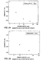
Since matching is of particular interest to analog and mixed signal designers,
Figure 24 shows the percent mismatch as a function of length for a fixed width resistor
and Figure 25 represents the same parameter as a function of width with a fixed length.
The data, as expected, show improved matching with increasing dimensions.
The feasibility of fabricating a high value polysilicon resistor with low TCR has
been demonstrated. The investigation has uncovered a relationship between ion species,
sheet resistance and TCR which can result in reduced process complexity, Since 800°C
RTA is a benign temperature for present bipolar processes, it is possible if desired to decouple
the resistor activation step from the RTA used to set the device electrical
parameters.
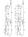
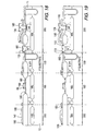
With the Bipolar and TCRL components processed to this point, it is now
appropriate to remove the protection layers from the CMOS portions of the wafer so that
the remaining metalization operations can be performed on all devices. Turning next to
Figure 16, the TCRL resistor 141 and the NPN transistor regions 200 are protected with a
layer of photoresist 160. The photoresist is patterned to open a region above the CMOS
devices 100. Next, the protective oxide 92 (Fig. 15) is removed.
Now refer to Figure 17. The photoresist layer 160 is removed, followed by removal
of the nitride protect layer 90. At this time, the emitter 170 and the resistor 141 are
subjected to an RTA step. The step is carried out at approximately 900°C for 0.5 minutes,
and completes the fabrication of the emitter first prepared in the steps shown previously
in Figure 13.
The screen oxide layer 80 over the lightly doped source and drain regions of the
CMOS device is then removed. As shown in Figure 18, the exposed polysilicon regions of
the resistor 141, the gate 66, the source and drain regions, and the collector and emitter
contacts 133, 134 are silicided with platinum 180 to form a platinum silicide layer on the
exposed polysilicon. As shown in Figure 19, a sidewall spacer oxide 190 is applied to the
sidewalls of the emitter contact 134 and the collector contact 133. The rest of the spacer
oxide is etched and removed, Thereafter, the substrate is subjected to suitable
metallization layers, including the formation of three metal layers separated from each
other by suitable insulating layers and separate layers being selectively interconnected,
one to the other, by the formation of vias that are filled with conductive material. After
metallization the entire device is covered with a passivation layer, typically silicon nitride,
and a substrate including the integrated circuits and devices made thereon are then
further processed for testing and assembly.
A low temperature coefficient resistor (TCRL) has some unrepaired ion implant
damage. The damaged portion raises the resistance and renders the resistor less sensitive
to operating temperature fluctuations. A polysilicon thin film low temperature coefficient
resistor and a method for the resistor's fabrication overcomes the coefficient of resistance
problem of the prior art, while at the same time eliminating steps from the BiCMOS
fabrication process, optimizing bipolar design tradeoffs, and improving passive device
isolation. A low temperature coefficient of resistance resistor (TCRL) is formed on a layer
of insulation, typically silicon dioxide or silicon nitride, the layer comprising polysilicon
having a relatively high concentration of dopants of one or more species. An annealing
process is used for the implanted resistor which is shorter than that for typical prior art
implanted resistors, leaving some intentional unannealed damage in the resistor. The
planned damage gives the TCRL a higher resistance without increasing its temperature
coefficient. A process for fabrication of the resistor is used which combines separate
spacer oxide depositions, provides buried layers having different diffusion coefficients,
incorporates dual dielectric trench sidewalls that double as a polish stop, supplies a spacer
structure that controls precisely the emitter-base dimension, and integrates bipolar and
CMOS devices with negligible compromise to the features of either type.