EP1062689B1 - Solarzellenanordnung und verfahren zur herstellung einer solarzellenanordnung - Google Patents
Solarzellenanordnung und verfahren zur herstellung einer solarzellenanordnung Download PDFInfo
- Publication number
- EP1062689B1 EP1062689B1 EP99920548A EP99920548A EP1062689B1 EP 1062689 B1 EP1062689 B1 EP 1062689B1 EP 99920548 A EP99920548 A EP 99920548A EP 99920548 A EP99920548 A EP 99920548A EP 1062689 B1 EP1062689 B1 EP 1062689B1
- Authority
- EP
- European Patent Office
- Prior art keywords
- solar cell
- subcells
- solar
- cell arrangement
- series
- Prior art date
- Legal status (The legal status is an assumption and is not a legal conclusion. Google has not performed a legal analysis and makes no representation as to the accuracy of the status listed.)
- Expired - Lifetime
Links
- 238000004519 manufacturing process Methods 0.000 title claims description 24
- 239000000463 material Substances 0.000 claims abstract description 56
- 239000004065 semiconductor Substances 0.000 claims abstract description 43
- 238000000034 method Methods 0.000 claims description 44
- 238000005530 etching Methods 0.000 claims description 21
- 239000012212 insulator Substances 0.000 claims description 17
- 238000007373 indentation Methods 0.000 claims description 14
- 239000004020 conductor Substances 0.000 claims description 9
- 239000011810 insulating material Substances 0.000 claims description 6
- XLYOFNOQVPJJNP-UHFFFAOYSA-N water Substances O XLYOFNOQVPJJNP-UHFFFAOYSA-N 0.000 claims description 2
- 238000009210 therapy by ultrasound Methods 0.000 claims 1
- 210000004027 cell Anatomy 0.000 description 221
- 235000012431 wafers Nutrition 0.000 description 131
- 239000010410 layer Substances 0.000 description 60
- 238000001465 metallisation Methods 0.000 description 41
- 239000000758 substrate Substances 0.000 description 41
- 150000004767 nitrides Chemical class 0.000 description 35
- HEMHJVSKTPXQMS-UHFFFAOYSA-M Sodium hydroxide Chemical compound [OH-].[Na+] HEMHJVSKTPXQMS-UHFFFAOYSA-M 0.000 description 24
- 238000009792 diffusion process Methods 0.000 description 24
- 229910052751 metal Inorganic materials 0.000 description 19
- 239000002184 metal Substances 0.000 description 19
- 238000005520 cutting process Methods 0.000 description 18
- 238000007650 screen-printing Methods 0.000 description 17
- XUIMIQQOPSSXEZ-UHFFFAOYSA-N Silicon Chemical compound [Si] XUIMIQQOPSSXEZ-UHFFFAOYSA-N 0.000 description 15
- 229910052710 silicon Inorganic materials 0.000 description 15
- 230000008569 process Effects 0.000 description 14
- 239000010703 silicon Substances 0.000 description 13
- 238000000926 separation method Methods 0.000 description 11
- 238000002955 isolation Methods 0.000 description 10
- 230000004888 barrier function Effects 0.000 description 9
- OAICVXFJPJFONN-UHFFFAOYSA-N Phosphorus Chemical compound [P] OAICVXFJPJFONN-UHFFFAOYSA-N 0.000 description 8
- 229910052782 aluminium Inorganic materials 0.000 description 8
- XAGFODPZIPBFFR-UHFFFAOYSA-N aluminium Chemical compound [Al] XAGFODPZIPBFFR-UHFFFAOYSA-N 0.000 description 8
- 230000015572 biosynthetic process Effects 0.000 description 8
- 238000000151 deposition Methods 0.000 description 8
- 230000008021 deposition Effects 0.000 description 8
- 238000005755 formation reaction Methods 0.000 description 8
- KRHYYFGTRYWZRS-UHFFFAOYSA-N hydrofluoric acid Substances F KRHYYFGTRYWZRS-UHFFFAOYSA-N 0.000 description 8
- 238000000623 plasma-assisted chemical vapour deposition Methods 0.000 description 8
- 239000004642 Polyimide Substances 0.000 description 7
- BQCADISMDOOEFD-UHFFFAOYSA-N Silver Chemical compound [Ag] BQCADISMDOOEFD-UHFFFAOYSA-N 0.000 description 7
- 238000005334 plasma enhanced chemical vapour deposition Methods 0.000 description 7
- 229920001721 polyimide Polymers 0.000 description 7
- 229910052709 silver Inorganic materials 0.000 description 7
- 239000004332 silver Substances 0.000 description 7
- 229910000679 solder Inorganic materials 0.000 description 7
- 238000011049 filling Methods 0.000 description 6
- 150000001875 compounds Chemical class 0.000 description 5
- 230000002950 deficient Effects 0.000 description 5
- 238000009413 insulation Methods 0.000 description 5
- 229910052698 phosphorus Inorganic materials 0.000 description 5
- 239000011574 phosphorus Substances 0.000 description 5
- 239000011248 coating agent Substances 0.000 description 4
- 238000000576 coating method Methods 0.000 description 4
- QPJSUIGXIBEQAC-UHFFFAOYSA-N n-(2,4-dichloro-5-propan-2-yloxyphenyl)acetamide Chemical compound CC(C)OC1=CC(NC(C)=O)=C(Cl)C=C1Cl QPJSUIGXIBEQAC-UHFFFAOYSA-N 0.000 description 4
- 239000000853 adhesive Substances 0.000 description 3
- 230000001070 adhesive effect Effects 0.000 description 3
- 238000003491 array Methods 0.000 description 3
- 239000002800 charge carrier Substances 0.000 description 3
- 229910021419 crystalline silicon Inorganic materials 0.000 description 3
- 239000000945 filler Substances 0.000 description 3
- 238000007639 printing Methods 0.000 description 3
- 238000005476 soldering Methods 0.000 description 3
- 239000007858 starting material Substances 0.000 description 3
- 239000000126 substance Substances 0.000 description 3
- 239000010409 thin film Substances 0.000 description 3
- 229910052581 Si3N4 Inorganic materials 0.000 description 2
- 238000004026 adhesive bonding Methods 0.000 description 2
- 239000010953 base metal Substances 0.000 description 2
- 239000000969 carrier Substances 0.000 description 2
- 238000006243 chemical reaction Methods 0.000 description 2
- 239000006059 cover glass Substances 0.000 description 2
- 230000007547 defect Effects 0.000 description 2
- 238000010292 electrical insulation Methods 0.000 description 2
- 238000005516 engineering process Methods 0.000 description 2
- 230000002349 favourable effect Effects 0.000 description 2
- 238000010304 firing Methods 0.000 description 2
- 239000012774 insulation material Substances 0.000 description 2
- 239000004922 lacquer Substances 0.000 description 2
- 230000000873 masking effect Effects 0.000 description 2
- 229910021421 monocrystalline silicon Inorganic materials 0.000 description 2
- 238000001020 plasma etching Methods 0.000 description 2
- 239000000243 solution Substances 0.000 description 2
- 239000002344 surface layer Substances 0.000 description 2
- GLGNXYJARSMNGJ-VKTIVEEGSA-N (1s,2s,3r,4r)-3-[[5-chloro-2-[(1-ethyl-6-methoxy-2-oxo-4,5-dihydro-3h-1-benzazepin-7-yl)amino]pyrimidin-4-yl]amino]bicyclo[2.2.1]hept-5-ene-2-carboxamide Chemical compound CCN1C(=O)CCCC2=C(OC)C(NC=3N=C(C(=CN=3)Cl)N[C@H]3[C@H]([C@@]4([H])C[C@@]3(C=C4)[H])C(N)=O)=CC=C21 GLGNXYJARSMNGJ-VKTIVEEGSA-N 0.000 description 1
- OKTJSMMVPCPJKN-UHFFFAOYSA-N Carbon Chemical compound [C] OKTJSMMVPCPJKN-UHFFFAOYSA-N 0.000 description 1
- RYGMFSIKBFXOCR-UHFFFAOYSA-N Copper Chemical compound [Cu] RYGMFSIKBFXOCR-UHFFFAOYSA-N 0.000 description 1
- 239000002253 acid Substances 0.000 description 1
- 239000012670 alkaline solution Substances 0.000 description 1
- 229910021417 amorphous silicon Inorganic materials 0.000 description 1
- 238000013459 approach Methods 0.000 description 1
- 230000000712 assembly Effects 0.000 description 1
- 238000000429 assembly Methods 0.000 description 1
- 238000010344 co-firing Methods 0.000 description 1
- 229940125758 compound 15 Drugs 0.000 description 1
- 229910052802 copper Inorganic materials 0.000 description 1
- 239000010949 copper Substances 0.000 description 1
- 230000008878 coupling Effects 0.000 description 1
- 238000010168 coupling process Methods 0.000 description 1
- 238000005859 coupling reaction Methods 0.000 description 1
- 239000013078 crystal Substances 0.000 description 1
- 230000006735 deficit Effects 0.000 description 1
- 230000001419 dependent effect Effects 0.000 description 1
- 230000006866 deterioration Effects 0.000 description 1
- 238000005553 drilling Methods 0.000 description 1
- 238000001312 dry etching Methods 0.000 description 1
- 230000000694 effects Effects 0.000 description 1
- 239000011152 fibreglass Substances 0.000 description 1
- 239000010408 film Substances 0.000 description 1
- 239000011521 glass Substances 0.000 description 1
- 229910002804 graphite Inorganic materials 0.000 description 1
- 239000010439 graphite Substances 0.000 description 1
- BHEPBYXIRTUNPN-UHFFFAOYSA-N hydridophosphorus(.) (triplet) Chemical compound [PH] BHEPBYXIRTUNPN-UHFFFAOYSA-N 0.000 description 1
- 230000010354 integration Effects 0.000 description 1
- 150000002500 ions Chemical class 0.000 description 1
- 238000005304 joining Methods 0.000 description 1
- 238000011031 large-scale manufacturing process Methods 0.000 description 1
- 230000007246 mechanism Effects 0.000 description 1
- 239000000203 mixture Substances 0.000 description 1
- 230000005693 optoelectronics Effects 0.000 description 1
- 239000003973 paint Substances 0.000 description 1
- 238000002161 passivation Methods 0.000 description 1
- 238000001782 photodegradation Methods 0.000 description 1
- 238000013082 photovoltaic technology Methods 0.000 description 1
- 238000005498 polishing Methods 0.000 description 1
- 229910021420 polycrystalline silicon Inorganic materials 0.000 description 1
- 238000005215 recombination Methods 0.000 description 1
- 230000006798 recombination Effects 0.000 description 1
- 230000009467 reduction Effects 0.000 description 1
- 230000000717 retained effect Effects 0.000 description 1
- HQVNEWCFYHHQES-UHFFFAOYSA-N silicon nitride Chemical compound N12[Si]34N5[Si]62N3[Si]51N64 HQVNEWCFYHHQES-UHFFFAOYSA-N 0.000 description 1
- 239000002904 solvent Substances 0.000 description 1
- 210000002023 somite Anatomy 0.000 description 1
- 238000000527 sonication Methods 0.000 description 1
- 230000036561 sun exposure Effects 0.000 description 1
- 239000002966 varnish Substances 0.000 description 1
- 238000003466 welding Methods 0.000 description 1
Images


Classifications
-
- H—ELECTRICITY
- H10—SEMICONDUCTOR DEVICES; ELECTRIC SOLID-STATE DEVICES NOT OTHERWISE PROVIDED FOR
- H10F—INORGANIC SEMICONDUCTOR DEVICES SENSITIVE TO INFRARED RADIATION, LIGHT, ELECTROMAGNETIC RADIATION OF SHORTER WAVELENGTH OR CORPUSCULAR RADIATION
- H10F77/00—Constructional details of devices covered by this subclass
- H10F77/10—Semiconductor bodies
- H10F77/14—Shape of semiconductor bodies; Shapes, relative sizes or dispositions of semiconductor regions within semiconductor bodies
- H10F77/147—Shapes of bodies
-
- B—PERFORMING OPERATIONS; TRANSPORTING
- B64—AIRCRAFT; AVIATION; COSMONAUTICS
- B64G—COSMONAUTICS; VEHICLES OR EQUIPMENT THEREFOR
- B64G1/00—Cosmonautic vehicles
- B64G1/22—Parts of, or equipment specially adapted for fitting in or to, cosmonautic vehicles
- B64G1/42—Arrangements or adaptations of power supply systems
- B64G1/44—Arrangements or adaptations of power supply systems using radiation, e.g. deployable solar arrays
- B64G1/443—Photovoltaic cell arrays
-
- H—ELECTRICITY
- H10—SEMICONDUCTOR DEVICES; ELECTRIC SOLID-STATE DEVICES NOT OTHERWISE PROVIDED FOR
- H10F—INORGANIC SEMICONDUCTOR DEVICES SENSITIVE TO INFRARED RADIATION, LIGHT, ELECTROMAGNETIC RADIATION OF SHORTER WAVELENGTH OR CORPUSCULAR RADIATION
- H10F10/00—Individual photovoltaic cells, e.g. solar cells
- H10F10/10—Individual photovoltaic cells, e.g. solar cells having potential barriers
- H10F10/14—Photovoltaic cells having only PN homojunction potential barriers
- H10F10/146—Back-junction photovoltaic cells, e.g. having interdigitated base-emitter regions on the back side
-
- H—ELECTRICITY
- H10—SEMICONDUCTOR DEVICES; ELECTRIC SOLID-STATE DEVICES NOT OTHERWISE PROVIDED FOR
- H10F—INORGANIC SEMICONDUCTOR DEVICES SENSITIVE TO INFRARED RADIATION, LIGHT, ELECTROMAGNETIC RADIATION OF SHORTER WAVELENGTH OR CORPUSCULAR RADIATION
- H10F19/00—Integrated devices, or assemblies of multiple devices, comprising at least one photovoltaic cell covered by group H10F10/00, e.g. photovoltaic modules
- H10F19/90—Structures for connecting between photovoltaic cells, e.g. interconnections or insulating spacers
- H10F19/902—Structures for connecting between photovoltaic cells, e.g. interconnections or insulating spacers for series or parallel connection of photovoltaic cells
- H10F19/904—Structures for connecting between photovoltaic cells, e.g. interconnections or insulating spacers for series or parallel connection of photovoltaic cells characterised by the shapes of the structures
-
- H—ELECTRICITY
- H10—SEMICONDUCTOR DEVICES; ELECTRIC SOLID-STATE DEVICES NOT OTHERWISE PROVIDED FOR
- H10F—INORGANIC SEMICONDUCTOR DEVICES SENSITIVE TO INFRARED RADIATION, LIGHT, ELECTROMAGNETIC RADIATION OF SHORTER WAVELENGTH OR CORPUSCULAR RADIATION
- H10F19/00—Integrated devices, or assemblies of multiple devices, comprising at least one photovoltaic cell covered by group H10F10/00, e.g. photovoltaic modules
- H10F19/90—Structures for connecting between photovoltaic cells, e.g. interconnections or insulating spacers
- H10F19/902—Structures for connecting between photovoltaic cells, e.g. interconnections or insulating spacers for series or parallel connection of photovoltaic cells
- H10F19/908—Structures for connecting between photovoltaic cells, e.g. interconnections or insulating spacers for series or parallel connection of photovoltaic cells for back-contact photovoltaic cells
-
- H—ELECTRICITY
- H10—SEMICONDUCTOR DEVICES; ELECTRIC SOLID-STATE DEVICES NOT OTHERWISE PROVIDED FOR
- H10F—INORGANIC SEMICONDUCTOR DEVICES SENSITIVE TO INFRARED RADIATION, LIGHT, ELECTROMAGNETIC RADIATION OF SHORTER WAVELENGTH OR CORPUSCULAR RADIATION
- H10F77/00—Constructional details of devices covered by this subclass
- H10F77/20—Electrodes
- H10F77/206—Electrodes for devices having potential barriers
- H10F77/211—Electrodes for devices having potential barriers for photovoltaic cells
- H10F77/219—Arrangements for electrodes of back-contact photovoltaic cells
- H10F77/227—Arrangements for electrodes of back-contact photovoltaic cells for emitter wrap-through [EWT] photovoltaic cells, e.g. interdigitated emitter-base back-contacts
-
- Y—GENERAL TAGGING OF NEW TECHNOLOGICAL DEVELOPMENTS; GENERAL TAGGING OF CROSS-SECTIONAL TECHNOLOGIES SPANNING OVER SEVERAL SECTIONS OF THE IPC; TECHNICAL SUBJECTS COVERED BY FORMER USPC CROSS-REFERENCE ART COLLECTIONS [XRACs] AND DIGESTS
- Y02—TECHNOLOGIES OR APPLICATIONS FOR MITIGATION OR ADAPTATION AGAINST CLIMATE CHANGE
- Y02E—REDUCTION OF GREENHOUSE GAS [GHG] EMISSIONS, RELATED TO ENERGY GENERATION, TRANSMISSION OR DISTRIBUTION
- Y02E10/00—Energy generation through renewable energy sources
- Y02E10/50—Photovoltaic [PV] energy
- Y02E10/547—Monocrystalline silicon PV cells
-
- Y—GENERAL TAGGING OF NEW TECHNOLOGICAL DEVELOPMENTS; GENERAL TAGGING OF CROSS-SECTIONAL TECHNOLOGIES SPANNING OVER SEVERAL SECTIONS OF THE IPC; TECHNICAL SUBJECTS COVERED BY FORMER USPC CROSS-REFERENCE ART COLLECTIONS [XRACs] AND DIGESTS
- Y10—TECHNICAL SUBJECTS COVERED BY FORMER USPC
- Y10S—TECHNICAL SUBJECTS COVERED BY FORMER USPC CROSS-REFERENCE ART COLLECTIONS [XRACs] AND DIGESTS
- Y10S439/00—Electrical connectors
- Y10S439/954—Special orientation of electrical connector
Definitions
- the present invention relates to a method and a device according to the respective preambles of the independent claims.
- the invention thus concerns a solar cell arrangement.
- solar cell arrays are also found in a variety of z.Zt. low-power small devices such as calculators and wristwatches.
- solar cell arrangements in devices of consumer goods electronics with a slightly higher power requirement than pocket calculators or watches.
- solar cell assemblies such as self-powered charging and operation of portable computers and cell phones, where operating voltages between 6 and 12V are common.
- a radiotelephone battery which provides about 2 watts for a call, requires a charging voltage of about 7 volts and a total charge of about 550mAh to 1200mAh.
- a charging voltage of about 7 volts and a total charge of about 550mAh to 1200mAh.
- solar cell arrangements In silicon technology, assuming an efficiency of only about 14% and small series circuit losses, this area achieves a voltage above about 7 volts and currents in excess of 100mA at the maximum power point so that it is possible in principle to allow a store by sufficiently long sun exposure.
- the cells to be used must not impair size and handiness, nor may they be too expensive to be used in the consumer goods sector.
- To meet the first requirement quite small solar cells of a few square centimeters must be interconnected, which requires micro modules instead of the usual in photovoltaic systems, large-scale solar cell modules. These must then be mounted inexpensively.
- the use of solar cell arrangements often fails due to the high cost. This was also due to the high cost of the series - i. Series connection.
- the base of the first cell In the series connection, in principle, the base of the first cell must be conductively connected to the emitter of the second cell.
- the base is typically arranged on one solar cell surface, the emitter on the opposite surface.
- the cell front side of a solar cell can be electrically conductively connected to the cell back side of the next cell via tinned copper tapes or the like. It's over KJ Euler, "Direct Energy Conversion", Verlag Karl Thiemig KG, Kunststoff, 1967, p.55 known . to arrange the individual solar cells such as shingles or roof tiles slightly overlapping and then electrically connect the base back contact of one cell with the emitter front contact on the next cell.
- U.S. Patent 4,612,408 For example, there is known an interconnected solar cell array which is fabricated by forming a plurality of devices on a semiconductor surface, forming grooves in surface that extend partially into the substrate, an oxide layer on selected portions of the one surface, and on the surfaces of the substrate Furrow is formed, the furrows are filled with an insulating material, metal joints are formed between adjacent building elements that extend across the furrows and extending the insulating material, attaching an insulating support to the one surface, and then separating through the wafer into the grooves from the other surface side to separate the adjacent devices while leaving the metal interconnects. Such a separation is problematic.
- a photovoltaic solar cell array is known that is monolithically fabricated without a supporting substrate by forming a network of trenches from one side of a substrate to define separate cell areas, filling the trenches with an insulating filler material that adheres to and imparts structural integrity to the substrate material Integrity, and then trenches are provided from the opposite side of the substrate to provide an air gap isolation network between adjacent cells.
- Series connections between adjacent cells are provided by connecting the front surface of one cell via the filler to the bulk semiconductor for the next cell, the connection being provided by the bulk semiconductor itself to back electrodes of each cell.
- the base is to contact via a small emitter-free area next to the trench filled with insulation material. This contacting results in only a small contacting area, which leads to high series resistances.
- polyimide is used as filling material, which represents a considerable cost factor in the production.
- U.S. Patent 5,164,019 For example, an array of series-connected cells formed in a monolithic semiconductor substrate and electrically isolated from one another by forming ridges partially passing through the substrate in a first surface between cells and then refracting the substrate from the bottom of the ruts to an opposing major surface , Metallization, which interconnects the cells, provides physical integrity of the cell field after the substrate has been broken.
- the furrows may be formed before completion of the production of the cells or after production of the cells. The problem is that the breaking of the cells must be defined and the mechanical stability must be ensured exclusively by typically thin metal contacts.
- an optoelectrically transmitting element and a method of making the same using a corrugated semiconductor substrate are known to produce an opto-electronically transmitted element.
- the element has a reduced effective thickness and improved optoelectronic conversion efficiency while maintaining its mechanical strength.
- a mold is provided which may be zigzag-shaped or meander-shaped in profile, these corrugated or corrugated structures are continuous.
- a flat component with a grid of through holes is known, wherein the through holes formed by the fact that on the front and back of a disc-shaped round body depending a number, preferably equidistant, parallel, in particular v-shaped trenches are incorporated, wherein the trenches of the two sides include an angle relative to each other and each are so deep that through holes are formed at the intersections of the trenches.
- the DE 44 263 47 deals primarily with the question of how such grids can be made. It is proposed to use, for example, monocrystalline silicon wafer wafers sawn from cast silicon blocks, multicrystalline silicon tapes produced by deposition from a silicon melt onto a graphite mesh, etc., as the compensation material. In the prior art document, the contact of the local solar cell is discussed, but no indication given how the tapped voltage can be easily increased by interconnecting multiple solar cells.
- a solar cell panel having a base structure comprising a metal substrate, an insulating layer over the substrate, and a layer of adhesive material over the insulating layer, wherein a panel of four rows of solar cells is arranged in parallel on the layer of adhesive material and the cells are arranged in that the p-layers of one cell row are adjacent to the n-layers of the next cell row.
- the cells are isolated and completely separated from each other and are connected to each other via metal strips.
- a bonding method is proposed to reduce power losses in the solar cell.
- a solar cell is to be formed from a semiconductor wafer, wherein the photosensitive semiconductor material has an upper and lower surface. Through the semiconductor wafer, holes are drawn from the top to the bottom, with which an electrical contact is made from the top to the bottom, wherein the contact brought down from the top is electrically isolated from the underside contact, so as to allow a current decrease.
- a particularly favorable series connection can be accomplished particularly favorably.
- a solar cell array consisting of a plurality of spaced elongated unit cells of a single wafer array, longitudinally ridged and made of a first conductivity type substrate material, with adjacent sidewalls of adjacent units in each inter-unitized groove.
- the sidewalls of each second groove are formed with regions of a second conductivity type such that there is only one connection between first and second conductivity types at or near the exposed surface of each device.
- the grooves extend all the way between the upper and lower wafer surfaces, forming discrete single units.
- every other groove ends near but in front of the top surface so as to define discrete double cell units.
- the units are connected in series by making ohmic connections between the region of the second conductivity type of one unit and the region of the first conductivity type of an adjacent unit.
- the furrows or gaps between the units can according to U.S. Patent 4,129,458 be filled with insulation material, or they remain partially or completely open, in which case a carrier to provide the relative orientation. As far as furrowing is concerned, it is only suggested that they do not extend completely from one surface to the other. So it can remain compounds that extend over the entire length of the adjacent page.
- U.S. Patent 4,283,589 Another arrangement of a semiconductor solar cell is known from U.S. Patent 4,283,589 known.
- a semiconductor solar cell is known from U.S. Patent 4,283,589 known.
- the grooves in the semiconductor substrate are also provided in order to enable a specific solar cell field circuit.
- cell units are formed from a single starting substrate in which grooves are provided by which adjacent cell units are spaced by a predetermined width.
- the grooves extend completely through the semiconductor wafer and mechanical integrity is provided either by filling the grooves with suitable material or by a supporting oxide layer running below the groove.
- a solar cell which comprises a plurality of discrete voltage-generating regions formed from a single semiconductor wafer and connected together so as to add the voltages of the single cells.
- the unit cells comprise doped regions of opposite conductivity types separated by a gap.
- These known solar cells are made by forming V-shaped grooves in the wafer and then aligning the wafer so that ions of a conductivity type are implanted on one side of the groove while the other side is shielded.
- a metallization layer is deposited and selectively etched away to provide interconnections between the unit cells.
- a solar cell which uses an anisotropically etched, specifically oriented silicon crystal wafer.
- the solar cell assembly includes upper edges between cell channel walls to improve the light trapping ability.
- the document is not concerned with the question of how to form and switch solar cell units from a single wafer so as to provide a higher voltage.
- a solar cell module which has a plurality of arranged on a support body and interconnected electrically interconnected single cells, wherein the support body is coextensive with the individual cells including the separation slots extending therebetween.
- the rear side contacts of the solar cells are electrically connected by contacting in the carrier body with associated terminal contact surfaces on the back of the carrier body.
- a carrier body for example, a glass fiber reinforced plastic can be used with a thickness of 0.3 mm.
- a terminal contact is applied and soldered to this a large-area solar cell, the area equal to the total unit of the carrier body.
- the semiconductor wafer mounted on the carrier body is divided by separating cuts, so that there is no need to handle each individual cell separately.
- the use and elaborate design of the carrier body are undesirable because they are costly.
- each solar cell array includes a plurality of series connected emitter-wrap-through type solar cells.
- damage to the solar cell is to be avoided, especially in space applications.
- a solar cell in a semiconductor substrate is known in which a certain type of contacting is prescribed without proposing to divide a larger semiconductor into a plurality of individual regions.
- the object of the present invention over the prior art is to provide a new solar cell array for industrial use to obtain a series-connected solar cell that enables cost-effective fabrication.
- a first basic idea of the invention is thus to provide a solar cell arrangement of series-connected solar subcells, which are formed from a semiconductor wafer base material, in which a plurality of recesses are provided for delimiting the individual, series-connected solar subcells, wherein at least some of the recesses extend from the top of the solar cell array to the bottom through the solar cell array and are left in continuation of the recesses to the side Solarzellenan alsskante out at this bridge webs to mechanically connect the solar sub-cells with each other.
- bridge bridges By means of these bridge bridges it is achieved that the respective solar subcells are electrically sufficiently separated from each other, but nevertheless a mechanical cohesion is given, which makes it possible to handle the solar cell arrangement like a single piece of material.
- the use of a few bridges bridges allows a much better isolation of the sub-cells with a much better stability. "Short-circuits" occur only locally and are not distributed over the entire subcell length.
- the bridge webs also eliminate the need for expensive filler material such as polyimide in a simple manner and can be formed so narrow that the electrical properties of the solar cell assembly is at most minimally affected. It is thus provided that a crystalline semiconductor wafer - preferably made of silicon - is used to produce all the cells of the solar cell array, wherein the electrical insulation of the sub-cells is carried out by partial thinning of the wafer.
- the partial thinning is such that the semiconductor material between two sub-cells is completely removed except for the remaining bridge webs and thus narrow elongated holes or slots are introduced into the wafer.
- a power bus is provided at the emitter and base of the fingergrid arranged such that two adjacent solar subcells electrically via a common busbar connected to each other. This busbar can run on the bridge bridges.
- an insulating material in particular an oxide layer, firmly connected therewith can be provided on the semiconductor material of the wafer, a conductor track being provided above this insulator layer.
- the solar cell arrangement can have solar subcells with at least two different areas, wherein, in particular, the subcells arranged on the edge in the area differ from the middle subcells.
- Such a design results in an increase in the efficiency of the overall arrangement. This is attributed to an incomplete isolation of the sub-cells, which causes a physical asymmetry.
- This asymmetry in turn means that the individual subcells are operated at different operating points, which means that, in contrast to conventional modules, in which the size of the individual cells is to be kept as equal as possible, a variation in the sizes of the individual subcells increases the efficiency can be.
- the lying on the edge and the negative pole of the solar cell assembly representing cell in their Surface is smaller than the remaining sub-cells. How large the area ratios are to be selected depends on the quality of the insulation between the sub-cells and the selected solar cell arrangement geometry. The better the insulation, the less the subcell area should differ. According to a preferred embodiment of the method of the present invention
- the bridge webs are designed to come into contact with an external component unit. prior to sawing the semiconductor wafer base material, a contact element is attached laterally. This makes it possible to completely cut through the semiconductor wafer base material in the most consistent way and to attach the bridge bridges externally by means of a connection strip to be applied laterally as an external component unit.
- the solar cell array can be formed of series-connected solar sub-cells, namely by producing the recesses by means of a wafer saw, laser, wire sawing, etching techniques, sandblasters, water jets, sonication or a combination of these techniques.
- the recesses may be produced by means of a wafer saw by gradually lowering it onto the wafer and moving it over it, wherein the wafer saw is preferably lowered at a first location onto the wafer base material, over the wafer base material until the beginning of the wafer Bridge web is moved, with a given reduction over the wafer base material at least once along the furrow is moved away, and then further lowered and moved again.
- the bridge bars can be formed without further, without the risk of breakage is essential.
- a wafer saw under preferably fast rotation controlled and / or controlled lowered onto the wafer, through the wafer base material and then across the wafer base material is moved across.
- the bridge webs can be encompassed by this contact strip.
- metal brackets may be provided, which provide an electrical connection of a respective subcell back contact to the front contact of another subcell and thus provide a series connection of the sub-cells, wherein they contain recesses through which separating tools can be passed.
- a further possibility, not claimed here, of achieving operability and isolation of series-connected solar subcells consists in arranging a semiconductor wafer on a carrier substrate and subsequently obtaining continuous cuts for the generation and isolation of the subcells.
- the carrier substrate may be formed for external wiring of the solar sub-cells and / or be provided with trenches through which separating tools can be guided to form recesses passing through the wafer, without damaging the carrier substrate itself.
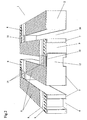
- the reference number 1 is used for the wafer; it is further referred to a solar subcell of 2, a back trench of 3, a recess of 4, an emitter contact finger of 5, a base contact metallization of 6, a front emitter of 7, a back emitter of 8, an emitter contact metallization of 9, a Dielectric or an insulator layer (nitride layer) than 10, a connection area than 12, a hole than 13, a cut area as 14, a contact connection as 15, a carrier substrate or a (carrier board) than 16, a conductor as 17, solder material than 18th , a substrate trench as 19, a contact clip as 20, a tab 21, a strip housing 22, a recess 23, and etch-resistant paint than 24.
- FIG. 1 and 2 a first embodiment of the invention is shown.
- the front emitter 7 are separated from each other.
- a small area of each sub cell back side is provided with an emitter (back emitter 8) .
- the front-side emitter 7 is connected to the rear-side emitter 8 via indentations 4 , likewise provided with an emitter layer, at the wafer edge.
- Both the back-exposed cell bases and the rear-side emitter regions 8 are each metallized spatially separated from each other, wherein by means of short busbars, ie contact 15 over the remaining connection regions 12 away a series connection of adjacent sub-cells 2 is made so as to allow a monolithic interconnection of the sub-cells 2 ,
- the rear busbar (contact connection 15) is applied by means of a screen printing paste, wherein the paste also fills the indentations 4 on the edge of the wafer.
- the indentations 4 filling metal forms an electrical connection between the applied on the cell front side emitter contact fingers 5 and the base metalization 6 of the adjacent subcell and thus ensures low series resistance losses.
- the contact connection 15 extends over an insulator layer 10 which is arranged to prevent a short circuit between the backside emitter 8 of a subcell and the cell base of the same subcell, on the other hand, increasing the distance between the backside emitter 8 of a subcell and the base contact metallization 6 of the adjacent subcell is.
- connection region 12 optionally a back trench 3 can be introduced.
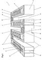
- the meandering miniature module ie solar cell arrangement geometry presented here, is advantageous because it enables a simple series connection of two subcells by means of a common busbar (contact connection 15) over the remaining connection regions 12 . But also comb-shaped geometries or arrangements with a plurality of bridge bridges (connecting regions 12) between two sub-cells can be realized. On the Fig. 11 will be referred to. There are miniature module geometries shown in plan view. Individual details of the solar cell assembly micro module, such as contact fingers and busbars, are not shown. The thick black lines represent the cuts 14 passing through the wafer, while the hatched areas mark the actual sub-cells 2 . White areas represent the bridge bridges 12.
- back-side trenches 3 (FIG. Fig. 3 ) be used. These are preferably to be introduced into the wafer already before the defect etching step (process step 1).
- indentations 4 Next can be dispensed with the formation of indentations 4 , if holes 13 are used to connect the front emitter 7 with the back instead; it is in Fig. 4 for the sake of simplicity, only one large hole is drawn in each case.
- the holes can be realized both with sawing techniques, such as crosswise double-sided sawing, as well as using pulsed lasers or ultrasonic drill in per se known manner.
- the inventive concept with the emitter-wrap-through technique.
- the front emitter 7 through many small holes 13, which are distributed over the entire subcell, plated on the back, as in Fig. 5 shown, for simplicity, only the position of some holes is indicated schematically and greatly enlarged.
- the holes are also on the cell backside ( Fig. 6 ) via strip-shaped emitter 8 connected to each other.
- the emitter contact metallization 9 is printed on the emitter strips, besides the base contact metallization 6 . It creates two interlocking devisgrids on the back of the cell.
- By using many holes distributed across the wafer the path of the carriers along the emitter to the metal contact is reduced, thereby reducing the series resistance of a subcell. Therefore, it may be possible to dispense with a front-side contacting of the emitter in this embodiment.
- the production and interconnection of the sub-cells is completely analogous to the process described above.
- the remaining bridge webs 12 can be realized by an insulating substance which makes a firm connection with the semiconductor, for example a polyimide.
- an insulating substance which makes a firm connection with the semiconductor
- the remaining bridge webs 12 can be realized by an insulating substance which makes a firm connection with the semiconductor, for example a polyimide.
- an insulating material for the entire bridge bridge eliminates the steps to the bedekkung the bridge bridge with an insulator or nitride layer. Otherwise, the process is analogous to the one described above.
- the mechanical stability through the bridges is absolutely sufficient for cell processing.
- the wafer thereby receives a certain elasticity and can thus easily be wound in itself.
- an insulator 10 serves to avoid a direct short circuit at the subcell edge where otherwise the base, emitter 7 and contact connection 15 touch.
- a polyimide or other insulator in the form of printing pastes may be used to prevent such a short circuit.
- Also in analogy to the first example illustrated with the first process may refer to a trench in the cell connection area 12 are dispensed with, if only by the application of an insulator layer 10 under the contact connection 15 of two sub-cells sufficient spatial separation of emitter and adjacent base contact is achieved.
- the masking in the nitride deposition after the emitter diffusion may be omitted if, in a subsequent exposure of the base contact surface, both the nitride and the underlying emitter layer are removed by means of planarization roller saws ( Fig. 8 ).
- connection areas (bridge bridges) 12 can be realized by an insulating substance which makes a firm connection with the semiconductor, such as a polyimide.
- a polyimide insulating substance which makes a firm connection with the semiconductor
- first the areas of the wafer in which the bridge bridges are to come zuo are removed. This can be done between process steps 3 and 4, for example. These areas are then partially filled with a polyimide.
- an insulating material for the entire bridge bridge eliminates the steps to cover the bridge bridge with an insulator or nitride layer. Otherwise, the process is analogous to the one described above.
- both the base 6 and the emitter contact metallization 9 of the sub-cells 2 are located on the side facing away from the light of the wafer.
- a front emitter is completely dispensed with ( Fig. 9 ).
- the mode of operation of a single subcell 2 corresponds to that of an "Interdigitated Back Contact" cell, which are used primarily in photovoltaic concentrator systems.
- On the lower cell back two metallization grids for emitter 9 and base contact 6 are interdigitated.
- the emitter region 8 is located directly below the metal fingers of the emitter contact grid 9 and is thus completely metallized.
- the contact grids cover almost the entire cell back; the remaining areas are covered with a dielectric or an insulator layer 10 and electronically passivated. Also, the cell front, which is free of any metallization, is covered by a passivating dielectric 10 .
- the absence of a front emitter reduces the probability of collection of charge carriers, so that for the production of the solar cell assembly micro module according to this variant, a high-quality semiconductor starting material with a correspondingly large carrier diffusion length must be used.
- One representative of such high-quality starting materials is monocrystalline silicon.
- connection connections 15 are designed analogously to the previous examples.
- the size of the heavily diffused emitter regions and the surface area of the base metal contacts can be reduced with the high recombination of charge carriers prevailing there.
- the dielectric for the emitter diffusion is opened only pointwise. Both the cell emitter and the cell base are contacted via regularly spaced metallization points. The individual points for emitter or base contact are electrically connected via two intermeshing contact grids, wherein the grid fingers extend on the dielectric.
- the structure of the sub-cells then corresponds to that of so-called "Point Contact Solar Cells".
- the production of a solar cell array micro module with subcells designed in this way can be analogous to the above-mentioned process sequence.
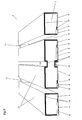
- Fig. 12-13 provides a further embodiment of the solar cell assembly micro module that the front-side emitter layer 7 of the sub-cell 2 is guided through the cutting regions 14 on the wafer back side.
- Filling the cutting area 14 with a conductive material ( Fig. 13g ) Permits direct interconnection of two sub-cells 2.
- the advantages of this embodiment are the need for additional holes or recesses in the sub-cells, the large-area series connection of two sub-cells and thus low series resistances in the module, as well as a very good mechanical stability by filling a large portion of the cutting areas.
- process step 5 is to be regarded as optional, since the n-layer removed thereby, due to the nitride layer 10 and the base metallization 6, is not in connection with the actual cell emitter 7 and is therefore inactive.
- Fig. 16 an embodiment results from an EWT design of the solar cell assembly micro module as follows.
- Base 6 and emitter contact metallization 9 of a subcell are located respectively on the cell backside and form an interlocking fingergrid.
- the intersections 14 are filled during the application of the emitter contact metallization 9 , so that during the subsequent application of the base metalization 6, a series connection of two adjacent sub-cells 2 is achieved by means of an overlap of the two metallizations in the intersection region 14 .
- Fig. 16a - 16j illustrate a possible manufacturing process.
- FIG. Fig. 17 Another variant, not claimed here, for producing a solar cell assembly micro module is based on the use of a carrier substrate or a carrier board 16 (FIG. Fig. 17 ) for the interconnection of the sub-cells.
- solar cells must be produced, the emitter and base contact come to rest on the back of the wafer.
- the cell designs presented in the previous examples such as "emitter-wrap-through” and "interdigitated back-contact solar cell” for Use come.
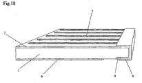
- the emitter-wrap-around cell concept is used. In this concept ( Fig. 18 ), the front emitter 7 is guided along a wafer edge on the back (back emitter 8) .
- the base contact metallization 6 is applied in strip form in accordance with the later geometry of the subcells, but without touching the rear emitter contact 9 .
- the carrier substrate 16 (FIG. Fig. 17 ), to which the solar cell is to be permanently attached, carries printed conductors 17, which create a connection between the base contact 6 and the back emitter contact 9 of the adjacent subcell ( Fig. 18 ).
- the cell If the cell is soldered to the substrate, then the cell comes to lie on the conductor tracks 17 at a height of several 100 .mu.m due to the soldering material 18 . Therefore, the cell can be divided with a silicon wafer saw later into sub-cells, which are then already interconnected and their bases are completely isolated from each other.
- the printed conductors can be defined by means of screen printing, since the carrier substrates can thus be easily matched by the cell manufacturer to the different fields of application. But also a direct generation of the solar cell assembly micro module on printed circuit boards of the electrical industry is possible.
- the substrates can already be equipped with trenches 19 (FIG. Fig. 19 ), in which the saw blades travel when cutting through the wafer, without reaching into the substrate 16 .
- emitter and base contacts have been routed to a wafer side in the previous examples to achieve series connection
- another variant provides that emitter and base contacts remain on separate wafer sides. This allows the use of commercially available solar cells to produce the solar cell array micro module. Due to possible negative consequences in a severing of metallization layers (eg impairment of the cutting tool, metal drag on the cutting edge with local short circuiting at the PN junction) the back contact and the busbars of the front grids should not be continuous, but according to the strip shape of the sub-cells have interruptions, along whose wafers can be thinned or separated. This means that, except for using other metallization printing screens, there is no need to intervene in an existing cell manufacturing process.
- the contacting of the sub-cells is in this case made as previously described before their separation by means of an external Verschaltungselements; Here, however, it takes place with a laterally applied to an edge contact strip.
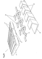
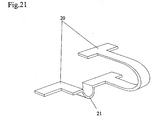
- the inside of the strip houses printed conductors and contact pins or metallic contact clips 20 (FIG. Fig. 20 ) Which each connect the back contact of a sub cell to the front contact of an adjacent sub cell.
- a film provided with tracks is conceivable as a bar or as part of such a bar.
- each individual contact clip 20 ( Fig. 21 ) consists in this embodiment of a bracket which includes the edge, and a metal strip lying perpendicular thereto, which contacts the back of an adjacent sub-cell.
- Each contact clip 20 has a tab 21 , through which the separating tools such as saw blades can be guided for producing the sub-cells. These tabs 21 simultaneously ensure a mechanically flexible connection of the sub-cells with each other.
- the front and top of the strip housing 22 is interrupted (recesses 23) to allow a separation of the wafer base material in sub-cells, for example by means of wafer saws.
- Two bars on opposite edges give the micro module increased stability, as well as a reduced series resistance and some redundancy in possibly defective execution of a solder joint.
- On the tabs 21 may be omitted if, as in Example 6, the wafer base material comes to rest by solder some 100 microns above its support surface and drive away the blades when separating over the temple ends.
Landscapes
- Engineering & Computer Science (AREA)
- Life Sciences & Earth Sciences (AREA)
- Sustainable Development (AREA)
- Remote Sensing (AREA)
- Aviation & Aerospace Engineering (AREA)
- Photovoltaic Devices (AREA)
Applications Claiming Priority (7)
| Application Number | Priority Date | Filing Date | Title |
|---|---|---|---|
| DE19810904 | 1998-03-13 | ||
| DE19810904 | 1998-03-13 | ||
| DE19824837 | 1998-06-04 | ||
| DE19824837 | 1998-06-04 | ||
| DE19836733 | 1998-08-13 | ||
| DE19836733 | 1998-08-13 | ||
| PCT/DE1999/000728 WO1999048136A2 (de) | 1998-03-13 | 1999-03-14 | Solarzellenanordnung |
Publications (2)
| Publication Number | Publication Date |
|---|---|
| EP1062689A2 EP1062689A2 (de) | 2000-12-27 |
| EP1062689B1 true EP1062689B1 (de) | 2009-09-09 |
Family
ID=27218208
Family Applications (1)
| Application Number | Title | Priority Date | Filing Date |
|---|---|---|---|
| EP99920548A Expired - Lifetime EP1062689B1 (de) | 1998-03-13 | 1999-03-14 | Solarzellenanordnung und verfahren zur herstellung einer solarzellenanordnung |
Country Status (5)
| Country | Link |
|---|---|
| US (1) | US6441297B1 (enExample) |
| EP (1) | EP1062689B1 (enExample) |
| JP (1) | JP2002507835A (enExample) |
| DE (3) | DE19980447D2 (enExample) |
| WO (1) | WO1999048136A2 (enExample) |
Families Citing this family (162)
| Publication number | Priority date | Publication date | Assignee | Title |
|---|---|---|---|---|
| US8664030B2 (en) | 1999-03-30 | 2014-03-04 | Daniel Luch | Collector grid and interconnect structures for photovoltaic arrays and modules |
| US20030192584A1 (en) * | 2002-01-25 | 2003-10-16 | Konarka Technologies, Inc. | Flexible photovoltaic cells and modules formed using foils |
| US6913713B2 (en) * | 2002-01-25 | 2005-07-05 | Konarka Technologies, Inc. | Photovoltaic fibers |
| US6706963B2 (en) * | 2002-01-25 | 2004-03-16 | Konarka Technologies, Inc. | Photovoltaic cell interconnection |
| US20050284513A1 (en) * | 2002-08-08 | 2005-12-29 | Christoph Brabec | Chip card comprising an integrated energy converter |
| US7186911B2 (en) | 2002-01-25 | 2007-03-06 | Konarka Technologies, Inc. | Methods of scoring for fabricating interconnected photovoltaic cells |
| US7414188B2 (en) | 2002-01-25 | 2008-08-19 | Konarka Technologies, Inc. | Co-sensitizers for dye sensitized solar cells |
| US6900382B2 (en) * | 2002-01-25 | 2005-05-31 | Konarka Technologies, Inc. | Gel electrolytes for dye sensitized solar cells |
| DE10020541A1 (de) * | 2000-04-27 | 2001-11-08 | Univ Konstanz | Verfahren zur Herstellung einer Solarzelle und Solarzelle |
| US6949400B2 (en) * | 2002-01-25 | 2005-09-27 | Konarka Technologies, Inc. | Ultrasonic slitting of photovoltaic cells and modules |
| US7205473B2 (en) * | 2002-01-25 | 2007-04-17 | Konarka Technologies, Inc. | Photovoltaic powered multimedia greeting cards and smart cards |
| US20030192585A1 (en) * | 2002-01-25 | 2003-10-16 | Konarka Technologies, Inc. | Photovoltaic cells incorporating rigid substrates |
| DE10047556A1 (de) * | 2000-09-22 | 2002-04-11 | Univ Konstanz | Verfahren zur Herstellung einer Solarzelle und nach diesem Verfahren hergestellte Solarzelle |
| AUPR174800A0 (en) * | 2000-11-29 | 2000-12-21 | Australian National University, The | Semiconductor processing |
| WO2003065393A2 (en) * | 2002-01-25 | 2003-08-07 | Konarka Technologies, Inc. | Displays with integrated photovoltaic cells |
| CA2474491A1 (en) * | 2002-01-25 | 2003-08-07 | Bill Beckenbaugh | Structures and materials for dye sensitized solar cells |
| EP1470563A2 (en) * | 2002-01-25 | 2004-10-27 | Konarka Technologies, Inc. | Photovoltaic cell components and materials |
| DE10239845C1 (de) * | 2002-08-29 | 2003-12-24 | Day4 Energy Inc | Elektrode für fotovoltaische Zellen, fotovoltaische Zelle und fotovoltaischer Modul |
| US7170001B2 (en) * | 2003-06-26 | 2007-01-30 | Advent Solar, Inc. | Fabrication of back-contacted silicon solar cells using thermomigration to create conductive vias |
| US7649141B2 (en) * | 2003-06-30 | 2010-01-19 | Advent Solar, Inc. | Emitter wrap-through back contact solar cells on thin silicon wafers |
| EP1711967A1 (en) * | 2004-01-23 | 2006-10-18 | Origin Energy Solar Pty Ltd. | Solar panel |
| US7335555B2 (en) * | 2004-02-05 | 2008-02-26 | Advent Solar, Inc. | Buried-contact solar cells with self-doping contacts |
| US20060060238A1 (en) * | 2004-02-05 | 2006-03-23 | Advent Solar, Inc. | Process and fabrication methods for emitter wrap through back contact solar cells |
| US20050172996A1 (en) * | 2004-02-05 | 2005-08-11 | Advent Solar, Inc. | Contact fabrication of emitter wrap-through back contact silicon solar cells |
| US7144751B2 (en) * | 2004-02-05 | 2006-12-05 | Advent Solar, Inc. | Back-contact solar cells and methods for fabrication |
| US8399331B2 (en) | 2007-10-06 | 2013-03-19 | Solexel | Laser processing for high-efficiency thin crystalline silicon solar cell fabrication |
| US8420435B2 (en) * | 2009-05-05 | 2013-04-16 | Solexel, Inc. | Ion implantation fabrication process for thin-film crystalline silicon solar cells |
| US8129822B2 (en) * | 2006-10-09 | 2012-03-06 | Solexel, Inc. | Template for three-dimensional thin-film solar cell manufacturing and methods of use |
| US9508886B2 (en) | 2007-10-06 | 2016-11-29 | Solexel, Inc. | Method for making a crystalline silicon solar cell substrate utilizing flat top laser beam |
| WO2007024898A2 (en) * | 2005-08-22 | 2007-03-01 | Konarka Technologies, Inc. | Displays with integrated photovoltaic cells |
| WO2007038297A2 (en) * | 2005-09-23 | 2007-04-05 | Tom Rust | Systems and methods for manufacturing photovoltaic devices |
| US20070079867A1 (en) * | 2005-10-12 | 2007-04-12 | Kethinni Chittibabu | Photovoltaic fibers |
| US8227688B1 (en) | 2005-10-17 | 2012-07-24 | Solaria Corporation | Method and resulting structure for assembling photovoltaic regions onto lead frame members for integration on concentrating elements for solar cells |
| US7910822B1 (en) | 2005-10-17 | 2011-03-22 | Solaria Corporation | Fabrication process for photovoltaic cell |
| US20070144577A1 (en) * | 2005-12-23 | 2007-06-28 | Rubin George L | Solar cell with physically separated distributed electrical contacts |
| WO2007087354A2 (en) * | 2006-01-24 | 2007-08-02 | Baer Stephen C | Cleaving wafers from silicon crystals |
| US7498508B2 (en) * | 2006-02-24 | 2009-03-03 | Day4 Energy, Inc. | High voltage solar cell and solar cell module |
| US8822810B2 (en) | 2006-04-13 | 2014-09-02 | Daniel Luch | Collector grid and interconnect structures for photovoltaic arrays and modules |
| US9006563B2 (en) | 2006-04-13 | 2015-04-14 | Solannex, Inc. | Collector grid and interconnect structures for photovoltaic arrays and modules |
| US8729385B2 (en) | 2006-04-13 | 2014-05-20 | Daniel Luch | Collector grid and interconnect structures for photovoltaic arrays and modules |
| US9236512B2 (en) | 2006-04-13 | 2016-01-12 | Daniel Luch | Collector grid and interconnect structures for photovoltaic arrays and modules |
| US8884155B2 (en) | 2006-04-13 | 2014-11-11 | Daniel Luch | Collector grid and interconnect structures for photovoltaic arrays and modules |
| US9865758B2 (en) | 2006-04-13 | 2018-01-09 | Daniel Luch | Collector grid and interconnect structures for photovoltaic arrays and modules |
| US20080083448A1 (en) * | 2006-09-29 | 2008-04-10 | Borden Peter G | Interconnect for thin film photovoltaic modules |
| US8035027B2 (en) | 2006-10-09 | 2011-10-11 | Solexel, Inc. | Solar module structures and assembly methods for pyramidal three-dimensional thin-film solar cells |
| US7999174B2 (en) * | 2006-10-09 | 2011-08-16 | Solexel, Inc. | Solar module structures and assembly methods for three-dimensional thin-film solar cells |
| US20080264477A1 (en) * | 2006-10-09 | 2008-10-30 | Soltaix, Inc. | Methods for manufacturing three-dimensional thin-film solar cells |
| US8512581B2 (en) * | 2006-10-09 | 2013-08-20 | Solexel, Inc. | Methods for liquid transfer coating of three-dimensional substrates |
| US20100304521A1 (en) * | 2006-10-09 | 2010-12-02 | Solexel, Inc. | Shadow Mask Methods For Manufacturing Three-Dimensional Thin-Film Solar Cells |
| US8035028B2 (en) * | 2006-10-09 | 2011-10-11 | Solexel, Inc. | Pyramidal three-dimensional thin-film solar cells |
| US8293558B2 (en) * | 2006-10-09 | 2012-10-23 | Solexel, Inc. | Method for releasing a thin-film substrate |
| US8193076B2 (en) | 2006-10-09 | 2012-06-05 | Solexel, Inc. | Method for releasing a thin semiconductor substrate from a reusable template |
| US20080092944A1 (en) * | 2006-10-16 | 2008-04-24 | Leonid Rubin | Semiconductor structure and process for forming ohmic connections to a semiconductor structure |
| CA2568136C (en) * | 2006-11-30 | 2008-07-29 | Tenxc Wireless Inc. | Butler matrix implementation |
| WO2008080160A1 (en) * | 2006-12-22 | 2008-07-03 | Advent Solar, Inc. | Interconnect technologies for back contact solar cells and modules |
| US20090056806A1 (en) * | 2007-09-05 | 2009-03-05 | Solaria Corporation | Solar cell structure including a plurality of concentrator elements with a notch design and predetermined radii and method |
| US7910392B2 (en) | 2007-04-02 | 2011-03-22 | Solaria Corporation | Method and system for assembling a solar cell package |
| US20080290368A1 (en) * | 2007-05-21 | 2008-11-27 | Day4 Energy, Inc. | Photovoltaic cell with shallow emitter |
| US8119902B2 (en) | 2007-05-21 | 2012-02-21 | Solaria Corporation | Concentrating module and method of manufacture for photovoltaic strips |
| WO2008157577A2 (en) * | 2007-06-18 | 2008-12-24 | E-Cube Technologies, Inc. | Methods and apparatuses for improving power extraction from solar cells |
| US7419377B1 (en) * | 2007-08-20 | 2008-09-02 | Solaria Corporation | Electrical coupling device and method for solar cells |
| WO2009064870A2 (en) * | 2007-11-13 | 2009-05-22 | Advent Solar, Inc. | Selective emitter and texture processes for back contact solar cells |
| US7910035B2 (en) | 2007-12-12 | 2011-03-22 | Solaria Corporation | Method and system for manufacturing integrated molded concentrator photovoltaic device |
| US20100275976A1 (en) * | 2007-12-18 | 2010-11-04 | Day4 Energy Inc. | Photovoltaic module with edge access to pv strings, interconnection method, apparatus, and system |
| US20100012172A1 (en) * | 2008-04-29 | 2010-01-21 | Advent Solar, Inc. | Photovoltaic Modules Manufactured Using Monolithic Module Assembly Techniques |
| US20100144080A1 (en) * | 2008-06-02 | 2010-06-10 | Solexel, Inc. | Method and apparatus to transfer coat uneven surface |
| AU2008359970A1 (en) * | 2008-07-28 | 2010-02-04 | Day4 Energy Inc. | Crystalline silicon PV cell with selective emitter produced with low temperature precision etch back and passivation process |
| US8101856B2 (en) * | 2008-10-02 | 2012-01-24 | International Business Machines Corporation | Quantum well GaP/Si tandem photovoltaic cells |
| US8916769B2 (en) | 2008-10-01 | 2014-12-23 | International Business Machines Corporation | Tandem nanofilm interconnected semiconductor wafer solar cells |
| US20100089390A1 (en) * | 2008-10-13 | 2010-04-15 | Sunlink, Corp | Solar array mounting system |
| US8288195B2 (en) * | 2008-11-13 | 2012-10-16 | Solexel, Inc. | Method for fabricating a three-dimensional thin-film semiconductor substrate from a template |
| EP2356675B1 (en) | 2008-11-13 | 2016-06-01 | Solexel, Inc. | Three dimensional thin film solar cell and manufacturing method thereof |
| KR100993511B1 (ko) | 2008-11-19 | 2010-11-12 | 엘지전자 주식회사 | 태양 전지 및 그 제조 방법 |
| EP2371006A4 (en) * | 2008-11-26 | 2013-05-01 | Solexel Inc | TRUNKED PYRAMID STRUCTURES FOR TRANSPARENT SOLAR CELLS |
| US9076642B2 (en) | 2009-01-15 | 2015-07-07 | Solexel, Inc. | High-Throughput batch porous silicon manufacturing equipment design and processing methods |
| US8906218B2 (en) | 2010-05-05 | 2014-12-09 | Solexel, Inc. | Apparatus and methods for uniformly forming porous semiconductor on a substrate |
| EP2387458B1 (en) * | 2009-01-15 | 2014-03-05 | Solexel, Inc. | Porous silicon electro-etching system and method |
| MY162405A (en) * | 2009-02-06 | 2017-06-15 | Solexel Inc | Trench Formation Method For Releasing A Thin-Film Substrate From A Reusable Semiconductor Template |
| US8621813B2 (en) * | 2009-03-06 | 2014-01-07 | Paul Dube | Wireless solar shingle panel and a method for implementing same |
| US8828517B2 (en) | 2009-03-23 | 2014-09-09 | Solexel, Inc. | Structure and method for improving solar cell efficiency and mechanical strength |
| CN102427971B (zh) * | 2009-04-14 | 2015-01-07 | 速力斯公司 | 高效外延化学气相沉积(cvd)反应器 |
| US9099584B2 (en) * | 2009-04-24 | 2015-08-04 | Solexel, Inc. | Integrated three-dimensional and planar metallization structure for thin film solar cells |
| KR101072543B1 (ko) * | 2009-04-28 | 2011-10-11 | 현대중공업 주식회사 | 태양 전지의 제조 방법 |
| MY165969A (en) | 2009-05-05 | 2018-05-18 | Solexel Inc | High-productivity porous semiconductor manufacturing equipment |
| US9318644B2 (en) | 2009-05-05 | 2016-04-19 | Solexel, Inc. | Ion implantation and annealing for thin film crystalline solar cells |
| US8445314B2 (en) * | 2009-05-22 | 2013-05-21 | Solexel, Inc. | Method of creating reusable template for detachable thin film substrate |
| EP2436028B1 (en) * | 2009-05-29 | 2016-08-10 | Solexel, Inc. | See-through three-dimensional thin-film solar cell semiconductor substrate and methods of manufacturing |
| US9012766B2 (en) | 2009-11-12 | 2015-04-21 | Silevo, Inc. | Aluminum grid as backside conductor on epitaxial silicon thin film solar cells |
| US8962380B2 (en) | 2009-12-09 | 2015-02-24 | Solexel, Inc. | High-efficiency photovoltaic back-contact solar cell structures and manufacturing methods using thin planar semiconductor absorbers |
| CN102844883B (zh) | 2010-02-12 | 2016-01-20 | 速力斯公司 | 用于制造光电池和微电子器件的半导体衬底的双面可重复使用的模板 |
| KR101369282B1 (ko) | 2010-06-09 | 2014-03-04 | 솔렉셀, 인크. | 고생산성 박막 증착 방법 및 시스템 |
| US9214576B2 (en) | 2010-06-09 | 2015-12-15 | Solarcity Corporation | Transparent conducting oxide for photovoltaic devices |
| MY158500A (en) | 2010-08-05 | 2016-10-14 | Solexel Inc | Backplane reinforcement and interconnects for solar cells |
| US9773928B2 (en) | 2010-09-10 | 2017-09-26 | Tesla, Inc. | Solar cell with electroplated metal grid |
| WO2012047269A1 (en) * | 2010-09-27 | 2012-04-12 | Banyan Energy, Inc. | Linear cell stringing |
| US9800053B2 (en) | 2010-10-08 | 2017-10-24 | Tesla, Inc. | Solar panels with integrated cell-level MPPT devices |
| US8196798B2 (en) | 2010-10-08 | 2012-06-12 | Kulicke And Soffa Industries, Inc. | Solar substrate ribbon bonding system |
| WO2012088481A2 (en) * | 2010-12-22 | 2012-06-28 | California Institute Of Technology | Heterojunction microwire array semiconductor devices |
| US9748414B2 (en) | 2011-05-20 | 2017-08-29 | Arthur R. Zingher | Self-activated front surface bias for a solar cell |
| USD699176S1 (en) | 2011-06-02 | 2014-02-11 | Solaria Corporation | Fastener for solar modules |
| US9054256B2 (en) | 2011-06-02 | 2015-06-09 | Solarcity Corporation | Tunneling-junction solar cell with copper grid for concentrated photovoltaic application |
| US9038329B2 (en) | 2011-10-11 | 2015-05-26 | Sunlink Corporation | Structure following roof mounted photovoltaic system |
| US9721984B2 (en) * | 2012-04-12 | 2017-08-01 | Taiwan Semiconductor Manufacturing Company, Ltd. | Image sensor manufacturing methods |
| US9065006B2 (en) * | 2012-05-11 | 2015-06-23 | Mtpv Power Corporation | Lateral photovoltaic device for near field use |
| EP2904643B1 (en) | 2012-10-04 | 2018-12-05 | SolarCity Corporation | Solar cell with electroplated metal grid |
| US9865754B2 (en) | 2012-10-10 | 2018-01-09 | Tesla, Inc. | Hole collectors for silicon photovoltaic cells |
| US10090430B2 (en) | 2014-05-27 | 2018-10-02 | Sunpower Corporation | System for manufacturing a shingled solar cell module |
| USD1009775S1 (en) | 2014-10-15 | 2024-01-02 | Maxeon Solar Pte. Ltd. | Solar panel |
| US9947820B2 (en) | 2014-05-27 | 2018-04-17 | Sunpower Corporation | Shingled solar cell panel employing hidden taps |
| USD933584S1 (en) | 2012-11-08 | 2021-10-19 | Sunpower Corporation | Solar panel |
| US9780253B2 (en) | 2014-05-27 | 2017-10-03 | Sunpower Corporation | Shingled solar cell module |
| US20140124014A1 (en) * | 2012-11-08 | 2014-05-08 | Cogenra Solar, Inc. | High efficiency configuration for solar cell string |
| CN103022204B (zh) * | 2012-12-12 | 2016-05-04 | 常州大学 | 一种背接触光伏组件焊带及其制备方法 |
| US9281436B2 (en) | 2012-12-28 | 2016-03-08 | Solarcity Corporation | Radio-frequency sputtering system with rotary target for fabricating solar cells |
| US9219174B2 (en) | 2013-01-11 | 2015-12-22 | Solarcity Corporation | Module fabrication of solar cells with low resistivity electrodes |
| US9412884B2 (en) | 2013-01-11 | 2016-08-09 | Solarcity Corporation | Module fabrication of solar cells with low resistivity electrodes |
| US10074755B2 (en) | 2013-01-11 | 2018-09-11 | Tesla, Inc. | High efficiency solar panel |
| DE102013200681A1 (de) * | 2013-01-17 | 2014-07-17 | Fraunhofer-Gesellschaft zur Förderung der angewandten Forschung e.V. | Referenzsolarzellenanordnung |
| US9624595B2 (en) | 2013-05-24 | 2017-04-18 | Solarcity Corporation | Electroplating apparatus with improved throughput |
| DE102013010691A1 (de) * | 2013-06-27 | 2014-12-31 | Nb Technologies Gmbh | Solarzelle |
| DE112014004468B4 (de) | 2013-09-25 | 2022-02-03 | Panasonic Intellectual Property Management Co., Ltd. | Solarzelle, Solarzellenmodul und Solarzellen-Herstellungsverfahren |
| US9496437B2 (en) | 2014-03-28 | 2016-11-15 | Sunpower Corporation | Solar cell having a plurality of sub-cells coupled by a metallization structure |
| US11482639B2 (en) | 2014-05-27 | 2022-10-25 | Sunpower Corporation | Shingled solar cell module |
| US11949026B2 (en) | 2014-05-27 | 2024-04-02 | Maxeon Solar Pte. Ltd. | Shingled solar cell module |
| US10309012B2 (en) | 2014-07-03 | 2019-06-04 | Tesla, Inc. | Wafer carrier for reducing contamination from carbon particles and outgassing |
| JP6337352B2 (ja) * | 2014-09-25 | 2018-06-06 | パナソニックIpマネジメント株式会社 | 太陽電池 |
| USD933585S1 (en) | 2014-10-15 | 2021-10-19 | Sunpower Corporation | Solar panel |
| USD896747S1 (en) | 2014-10-15 | 2020-09-22 | Sunpower Corporation | Solar panel |
| USD913210S1 (en) | 2014-10-15 | 2021-03-16 | Sunpower Corporation | Solar panel |
| USD999723S1 (en) | 2014-10-15 | 2023-09-26 | Sunpower Corporation | Solar panel |
| US10236406B2 (en) | 2014-12-05 | 2019-03-19 | Solarcity Corporation | Systems and methods for targeted annealing of photovoltaic structures |
| US9991412B2 (en) | 2014-12-05 | 2018-06-05 | Solarcity Corporation | Systems for precision application of conductive adhesive paste on photovoltaic structures |
| US10043937B2 (en) | 2014-12-05 | 2018-08-07 | Solarcity Corporation | Systems and method for precision automated placement of backsheet on PV modules |
| US9899546B2 (en) | 2014-12-05 | 2018-02-20 | Tesla, Inc. | Photovoltaic cells with electrodes adapted to house conductive paste |
| US9590132B2 (en) | 2014-12-05 | 2017-03-07 | Solarcity Corporation | Systems and methods for cascading photovoltaic structures |
| US9685579B2 (en) | 2014-12-05 | 2017-06-20 | Solarcity Corporation | Photovoltaic structure cleaving system |
| US10056522B2 (en) | 2014-12-05 | 2018-08-21 | Solarcity Corporation | System and apparatus for precision automation of tab attachment for fabrications of solar panels |
| US9947822B2 (en) | 2015-02-02 | 2018-04-17 | Tesla, Inc. | Bifacial photovoltaic module using heterojunction solar cells |
| US10861999B2 (en) | 2015-04-21 | 2020-12-08 | Sunpower Corporation | Shingled solar cell module comprising hidden tap interconnects |
| WO2017030695A1 (en) | 2015-08-18 | 2017-02-23 | Sunpower Corporation | Solar panel |
| US9761744B2 (en) | 2015-10-22 | 2017-09-12 | Tesla, Inc. | System and method for manufacturing photovoltaic structures with a metal seed layer |
| US9842956B2 (en) | 2015-12-21 | 2017-12-12 | Tesla, Inc. | System and method for mass-production of high-efficiency photovoltaic structures |
| US9496429B1 (en) | 2015-12-30 | 2016-11-15 | Solarcity Corporation | System and method for tin plating metal electrodes |
| MX389031B (es) | 2016-02-08 | 2025-03-20 | Mtpv Power Corp | Sistema termofotovoltaico de intervalo micrometrico radiativo con emisor transparente |
| US10115838B2 (en) | 2016-04-19 | 2018-10-30 | Tesla, Inc. | Photovoltaic structures with interlocking busbars |
| US10673379B2 (en) | 2016-06-08 | 2020-06-02 | Sunpower Corporation | Systems and methods for reworking shingled solar cell modules |
| US11437533B2 (en) | 2016-09-14 | 2022-09-06 | The Boeing Company | Solar cells for a solar cell array |
| US20180076349A1 (en) | 2016-09-14 | 2018-03-15 | The Boeing Company | Power routing module for a solar cell array |
| US9960305B2 (en) | 2016-09-21 | 2018-05-01 | The United States Of America As Represented By Secretary Of The Navy | Manufacture of solar concentrator modules using a wafer precursor |
| US20180358491A1 (en) * | 2017-06-12 | 2018-12-13 | The Boeing Company | Solar cell array with bypassed solar cells |
| US12490523B2 (en) * | 2017-06-12 | 2025-12-02 | The Boeing Company | Solar cell array with changeable string length |
| US10672919B2 (en) | 2017-09-19 | 2020-06-02 | Tesla, Inc. | Moisture-resistant solar cells for solar roof tiles |
| US11190128B2 (en) | 2018-02-27 | 2021-11-30 | Tesla, Inc. | Parallel-connected solar roof tile modules |
| US12244265B2 (en) | 2018-03-28 | 2025-03-04 | The Boeing Company | Wiring for a rigid panel solar array |
| US11967923B2 (en) | 2018-03-28 | 2024-04-23 | The Boeing Company | Single sheet foldout solar array |
| US11495698B2 (en) * | 2018-04-06 | 2022-11-08 | Sunpower Corporation | Reconfigurable photovoltaic laminate(s) and photovoltaic panel(s) |
| US11145774B2 (en) * | 2018-05-30 | 2021-10-12 | Solar Inventions Llc | Configurable solar cells |
| PL3576161T3 (pl) * | 2018-05-30 | 2021-11-08 | Centrum Badań I Rozwoju Technologii Dla Przemysłu Spółka Akcyjna | Bezkrzemowe ogniwo fotowoltaiczne, element budowlany oraz sposób wytwarzania bezkrzemowych ogniw fotowoltaicznych |
| US11496089B2 (en) | 2020-04-13 | 2022-11-08 | The Boeing Company | Stacked solar array |
| US12003210B2 (en) | 2020-04-13 | 2024-06-04 | The Boeing Company | Solar array attachment |
| US11377758B2 (en) | 2020-11-23 | 2022-07-05 | Stephen C. Baer | Cleaving thin wafers from crystals |
| CN116169121A (zh) * | 2022-12-28 | 2023-05-26 | 中润新能源(徐州)有限公司 | 一种能够降低切割损失的太阳能电池 |
Family Cites Families (26)
| Publication number | Priority date | Publication date | Assignee | Title |
|---|---|---|---|---|
| US2911539A (en) * | 1957-12-18 | 1959-11-03 | Bell Telephone Labor Inc | Photocell array |
| US3411952A (en) | 1962-04-02 | 1968-11-19 | Globe Union Inc | Photovoltaic cell and solar cell panel |
| US3330700A (en) | 1963-06-17 | 1967-07-11 | Electro Optical Systems Inc | Solar-cell panels |
| US3903427A (en) | 1973-12-28 | 1975-09-02 | Hughes Aircraft Co | Solar cell connections |
| GB1553356A (en) | 1976-12-27 | 1979-09-26 | Hamasawa Kogyo Kk | Solar battery |
| US4179318A (en) | 1978-02-13 | 1979-12-18 | Massachusetts Institute Of Technology | Method of making a solar-cell array |
| US4129458A (en) | 1978-02-13 | 1978-12-12 | Massachusetts Institute Of Technology | Solar-cell array |
| US4283589A (en) | 1978-05-01 | 1981-08-11 | Massachusetts Institute Of Technology | High-intensity, solid-state solar cell |
| US4352948A (en) * | 1979-09-07 | 1982-10-05 | Massachusetts Institute Of Technology | High-intensity solid-state solar-cell device |
| US4300680A (en) | 1980-05-12 | 1981-11-17 | Packaging Corporation Of America | Article carrier |
| US4376872A (en) | 1980-12-24 | 1983-03-15 | The United States Of America As Represented By The Administrator Of The National Aeronautics And Space Administration | High voltage V-groove solar cell |
| US4612408A (en) * | 1984-10-22 | 1986-09-16 | Sera Solar Corporation | Electrically isolated semiconductor integrated photodiode circuits and method |
| DE3529341A1 (de) | 1985-08-16 | 1987-02-19 | Telefunken Electronic Gmbh | Solarzellen-modul |
| DE3708548A1 (de) * | 1987-03-17 | 1988-09-29 | Telefunken Electronic Gmbh | Solarzellenmodul mit parallel und seriell angeordneten solarzellen |
| WO1989005521A1 (en) | 1987-12-03 | 1989-06-15 | Spectrolab, Inc. | Solar cell panel |
| JPH01181577A (ja) * | 1988-01-12 | 1989-07-19 | Kanegafuchi Chem Ind Co Ltd | 光半導体素子 |
| US4808904A (en) * | 1988-01-25 | 1989-02-28 | Solarex Corporation | Portable photovoltaic battery recharger |
| US5024953A (en) | 1988-03-22 | 1991-06-18 | Hitachi, Ltd. | Method for producing opto-electric transducing element |
| US5067985A (en) | 1990-06-08 | 1991-11-26 | The United States Of America As Represented By The Secretary Of The Air Force | Back-contact vertical-junction solar cell and method |
| US5164019A (en) | 1991-07-31 | 1992-11-17 | Sunpower Corporation | Monolithic series-connected solar cells having improved cell isolation and method of making same |
| US5330918A (en) * | 1992-08-31 | 1994-07-19 | The United States Of America As Represented By The Secretary Of The Navy | Method of forming a high voltage silicon-on-sapphire photocell array |
| US5538902A (en) * | 1993-06-29 | 1996-07-23 | Sanyo Electric Co., Ltd. | Method of fabricating a photovoltaic device having a three-dimensional shape |
| EP0742959B1 (de) | 1993-07-29 | 2001-11-14 | Gerhard Willeke | Verfahren zur Herstellung einer Solarzelle, sowie nach diesem verfahren hergestellte Solarzelle |
| US5391236A (en) * | 1993-07-30 | 1995-02-21 | Spectrolab, Inc. | Photovoltaic microarray structure and fabrication method |
| US5641362A (en) | 1995-11-22 | 1997-06-24 | Ebara Solar, Inc. | Structure and fabrication process for an aluminum alloy junction self-aligned back contact silicon solar cell |
| EP0881694A1 (en) | 1997-05-30 | 1998-12-02 | Interuniversitair Micro-Elektronica Centrum Vzw | Solar cell and process of manufacturing the same |
-
1999
- 1999-03-14 WO PCT/DE1999/000728 patent/WO1999048136A2/de not_active Ceased
- 1999-03-14 EP EP99920548A patent/EP1062689B1/de not_active Expired - Lifetime
- 1999-03-14 DE DE19980447T patent/DE19980447D2/de not_active Expired - Fee Related
- 1999-03-14 JP JP2000537249A patent/JP2002507835A/ja active Pending
- 1999-03-14 DE DE59915079T patent/DE59915079D1/de not_active Expired - Lifetime
- 1999-03-14 US US09/623,996 patent/US6441297B1/en not_active Expired - Fee Related
- 1999-03-15 DE DE19912980A patent/DE19912980A1/de not_active Withdrawn
Also Published As
| Publication number | Publication date |
|---|---|
| DE59915079D1 (de) | 2009-10-22 |
| JP2002507835A (ja) | 2002-03-12 |
| DE19980447D2 (de) | 2001-04-12 |
| US6441297B1 (en) | 2002-08-27 |
| WO1999048136A2 (de) | 1999-09-23 |
| EP1062689A2 (de) | 2000-12-27 |
| WO1999048136A3 (de) | 1999-11-11 |
| DE19912980A1 (de) | 1999-12-30 |
Similar Documents
| Publication | Publication Date | Title |
|---|---|---|
| EP1062689B1 (de) | Solarzellenanordnung und verfahren zur herstellung einer solarzellenanordnung | |
| EP0905794B1 (de) | Solarzelle und Herstellungsverfahren | |
| EP2033228B1 (de) | Einseitig kontaktierte solarzelle mit durchkontaktierungen und verfahren zur herstellung | |
| EP2308090B1 (de) | Einseitig kontaktiertes dünnschicht-solarmodul mit einer inneren kontaktschicht. | |
| DE69631815T2 (de) | Struktur und Herstellungsverfahren einer Solarzelle mit selbstausgerichtetem Rückseitenkontakt aus einer Aluminiumlegierung | |
| EP1421629B1 (de) | Solarzelle sowie verfahren zur herstellung einer solchen | |
| DE102005025125B4 (de) | Verfahren zur Herstellung einer einseitig kontaktierten Solarzelle und einseitig kontaktierte Solarzelle | |
| DE3727826A1 (de) | Serienverschaltetes duennschicht-solarmodul aus kristallinem silizium | |
| EP3084841B1 (de) | Photovoltaikmodul | |
| DE102011075352A1 (de) | Verfahren zum Rückseitenkontaktieren einer Silizium-Solarzelle und Silizium-Solarzelle mit einer solchen Rückseitenkontaktierung | |
| DE102013204923A1 (de) | Photovoltaikmodul | |
| DE102011000753A1 (de) | Solarzelle, Solarmodul und Verfahren zum Herstellen einer Solarzelle | |
| WO2011067338A2 (de) | Solarzelle, solarmodul und herstellungsverfahren für eine solarzelle bzw. für ein solarmodul | |
| EP0657067A1 (de) | Solarzellensystem | |
| DE102008021355B4 (de) | Verfahren zur Herstellung monokristalliner Solarzellen mit rückseitiger Kontaktstruktur | |
| DE2723620A1 (de) | Photozellenanordnung und verfahren zu ihrer herstellung | |
| DE202013012571U1 (de) | Herstellungsanlage zur Herstellung eines Photovoltaikmoduls sowie Photovoltaikmodul | |
| EP2718979B1 (de) | Dünnschicht-solarmodul mit integrierter verschaltung sowie verfahren zu dessen herstellung | |
| DE4143084A1 (de) | Verfahren zur herstellung einer solarzelle sowie solarzelle | |
| DE102010016976A1 (de) | Verfahren zum Verschalten von Solarzellen sowie Solarzellenverschaltung | |
| KR20210013950A (ko) | 슁글드 태양광 패널용 태양전지 셀의 제조방법 및 이를 이용한 태양광 패널 | |
| WO2012130392A1 (de) | Herstellung eines halbleiter-bauelements durch laser-unterstütztes bonden | |
| DE19651655C2 (de) | Verschaltete Solarzellen, insbesondere seriell verschaltete Dünnschicht-Solarmodule, und Verfahren zu ihrer Herstellung | |
| WO2025093166A1 (de) | Rückseitenkontaktierte solarzelle und verfahren zum herstellen einer rückseitenkontaktierten solarzelle | |
| WO2011020205A1 (de) | Vorrichtung und verfahren zur kontaktierung von siliziumsolarzellen |
Legal Events
| Date | Code | Title | Description |
|---|---|---|---|
| PUAI | Public reference made under article 153(3) epc to a published international application that has entered the european phase |
Free format text: ORIGINAL CODE: 0009012 |
|
| 17P | Request for examination filed |
Effective date: 20001013 |
|
| AK | Designated contracting states |
Kind code of ref document: A2 Designated state(s): CH DE ES FI FR GB IT LI NL SE |
|
| 17Q | First examination report despatched |
Effective date: 20040213 |
|
| RAP1 | Party data changed (applicant data changed or rights of an application transferred) |
Owner name: WILLEKE, GERHARD, DR. Owner name: FATH, PETER, DR. |
|
| RIN1 | Information on inventor provided before grant (corrected) |
Inventor name: STEFFEN KELLER |
|
| RIC1 | Information provided on ipc code assigned before grant |
Ipc: H01L 31/0352 20060101ALI20081120BHEP Ipc: H01L 31/05 20060101AFI20081120BHEP |
|
| RTI1 | Title (correction) |
Free format text: SOLAR CELL ARRANGEMENT AND METHOD OF MAKING A SOLAR CELL ARRANGEMENT |
|
| GRAP | Despatch of communication of intention to grant a patent |
Free format text: ORIGINAL CODE: EPIDOSNIGR1 |
|
| GRAS | Grant fee paid |
Free format text: ORIGINAL CODE: EPIDOSNIGR3 |
|
| GRAA | (expected) grant |
Free format text: ORIGINAL CODE: 0009210 |
|
| RIN1 | Information on inventor provided before grant (corrected) |
Inventor name: KELLER, STEFFEN |
|
| AK | Designated contracting states |
Kind code of ref document: B1 Designated state(s): CH DE ES FI FR GB IT LI NL SE |
|
| REG | Reference to a national code |
Ref country code: GB Ref legal event code: FG4D Free format text: NOT ENGLISH |
|
| REG | Reference to a national code |
Ref country code: CH Ref legal event code: EP |
|
| REF | Corresponds to: |
Ref document number: 59915079 Country of ref document: DE Date of ref document: 20091022 Kind code of ref document: P |
|
| PG25 | Lapsed in a contracting state [announced via postgrant information from national office to epo] |
Ref country code: SE Free format text: LAPSE BECAUSE OF FAILURE TO SUBMIT A TRANSLATION OF THE DESCRIPTION OR TO PAY THE FEE WITHIN THE PRESCRIBED TIME-LIMIT Effective date: 20090909 Ref country code: FI Free format text: LAPSE BECAUSE OF FAILURE TO SUBMIT A TRANSLATION OF THE DESCRIPTION OR TO PAY THE FEE WITHIN THE PRESCRIBED TIME-LIMIT Effective date: 20090909 |
|
| NLV1 | Nl: lapsed or annulled due to failure to fulfill the requirements of art. 29p and 29m of the patents act | ||
| PG25 | Lapsed in a contracting state [announced via postgrant information from national office to epo] |
Ref country code: NL Free format text: LAPSE BECAUSE OF FAILURE TO SUBMIT A TRANSLATION OF THE DESCRIPTION OR TO PAY THE FEE WITHIN THE PRESCRIBED TIME-LIMIT Effective date: 20090909 |
|
| PG25 | Lapsed in a contracting state [announced via postgrant information from national office to epo] |
Ref country code: ES Free format text: LAPSE BECAUSE OF FAILURE TO SUBMIT A TRANSLATION OF THE DESCRIPTION OR TO PAY THE FEE WITHIN THE PRESCRIBED TIME-LIMIT Effective date: 20091220 |
|
| PLBE | No opposition filed within time limit |
Free format text: ORIGINAL CODE: 0009261 |
|
| STAA | Information on the status of an ep patent application or granted ep patent |
Free format text: STATUS: NO OPPOSITION FILED WITHIN TIME LIMIT |
|
| 26N | No opposition filed |
Effective date: 20100610 |
|
| REG | Reference to a national code |
Ref country code: FR Ref legal event code: ST Effective date: 20101130 |
|
| REG | Reference to a national code |
Ref country code: CH Ref legal event code: NV Representative=s name: ISLER & PEDRAZZINI AG |
|
| PG25 | Lapsed in a contracting state [announced via postgrant information from national office to epo] |
Ref country code: FR Free format text: LAPSE BECAUSE OF NON-PAYMENT OF DUE FEES Effective date: 20100331 |
|
| PG25 | Lapsed in a contracting state [announced via postgrant information from national office to epo] |
Ref country code: IT Free format text: LAPSE BECAUSE OF FAILURE TO SUBMIT A TRANSLATION OF THE DESCRIPTION OR TO PAY THE FEE WITHIN THE PRESCRIBED TIME-LIMIT Effective date: 20090909 |
|
| PGFP | Annual fee paid to national office [announced via postgrant information from national office to epo] |
Ref country code: GB Payment date: 20110329 Year of fee payment: 13 |
|
| PGFP | Annual fee paid to national office [announced via postgrant information from national office to epo] |
Ref country code: CH Payment date: 20120329 Year of fee payment: 14 |
|
| PGFP | Annual fee paid to national office [announced via postgrant information from national office to epo] |
Ref country code: DE Payment date: 20120530 Year of fee payment: 14 |
|
| GBPC | Gb: european patent ceased through non-payment of renewal fee |
Effective date: 20120314 |
|
| PG25 | Lapsed in a contracting state [announced via postgrant information from national office to epo] |
Ref country code: GB Free format text: LAPSE BECAUSE OF NON-PAYMENT OF DUE FEES Effective date: 20120314 |
|
| REG | Reference to a national code |
Ref country code: CH Ref legal event code: PL |
|
| REG | Reference to a national code |
Ref country code: DE Ref legal event code: R119 Ref document number: 59915079 Country of ref document: DE Effective date: 20131001 |
|
| PG25 | Lapsed in a contracting state [announced via postgrant information from national office to epo] |
Ref country code: CH Free format text: LAPSE BECAUSE OF NON-PAYMENT OF DUE FEES Effective date: 20130331 Ref country code: LI Free format text: LAPSE BECAUSE OF NON-PAYMENT OF DUE FEES Effective date: 20130331 Ref country code: DE Free format text: LAPSE BECAUSE OF NON-PAYMENT OF DUE FEES Effective date: 20131001 |