EP1060444B1 - Chassis zur aufnahme von elektronikkarten - Google Patents
Chassis zur aufnahme von elektronikkarten Download PDFInfo
- Publication number
- EP1060444B1 EP1060444B1 EP99911585A EP99911585A EP1060444B1 EP 1060444 B1 EP1060444 B1 EP 1060444B1 EP 99911585 A EP99911585 A EP 99911585A EP 99911585 A EP99911585 A EP 99911585A EP 1060444 B1 EP1060444 B1 EP 1060444B1
- Authority
- EP
- European Patent Office
- Prior art keywords
- plug
- connection wall
- wall
- chassis
- electronic cards
- Prior art date
- Legal status (The legal status is an assumption and is not a legal conclusion. Google has not performed a legal analysis and makes no representation as to the accuracy of the status listed.)
- Expired - Lifetime
Links
Images


Classifications
-
- H—ELECTRICITY
- H05—ELECTRIC TECHNIQUES NOT OTHERWISE PROVIDED FOR
- H05K—PRINTED CIRCUITS; CASINGS OR CONSTRUCTIONAL DETAILS OF ELECTRIC APPARATUS; MANUFACTURE OF ASSEMBLAGES OF ELECTRICAL COMPONENTS
- H05K7/00—Constructional details common to different types of electric apparatus
- H05K7/14—Mounting supporting structure in casing or on frame or rack
- H05K7/1422—Printed circuit boards receptacles, e.g. stacked structures, electronic circuit modules or box like frames
- H05K7/1424—Card cages
-
- G—PHYSICS
- G06—COMPUTING OR CALCULATING; COUNTING
- G06F—ELECTRIC DIGITAL DATA PROCESSING
- G06F13/00—Interconnection of, or transfer of information or other signals between, memories, input/output devices or central processing units
- G06F13/38—Information transfer, e.g. on bus
- G06F13/40—Bus structure
- G06F13/4063—Device-to-bus coupling
- G06F13/409—Mechanical coupling
Definitions
- the invention relates to a chassis for receiving electronic cards according to the preamble of claim 1.
- a circuit board arrangement is also known from US Pat. No. 5,754,406. in the case of the one of the slots arranged in parallel Printed circuit boards, two U-shaped protective brackets each are the circuit boards in between shield on both sides.
- the invention has for its object a chassis train the above type so that when inserted or removing an electronic card damage same or from neighboring cards with simple means reliably can be avoided.
- the plug-in wall can be a chassis wall, which is only the mating connector carries, or be a motherboard that itself is equipped with electronic components. in the the latter case, it is useful if the motherboard through a protective plate made of an insulating material is covered, the openings for the mating connector or has the connector, so that the main board when inserting or removing electronic cards is secured against damage.
- the partitions can on the wall or on the Protective plate to be attached.
- the connection of the partitions with the plug-in wall or protective plate can be easily Way done in that the partitions on their respective at least one edge facing the wall Have hooks that can be engaged in one in the wall or the complementary opening formed the protective plate is. This is a simple assembly of the partitions possible. In the assembled position, the partitions can with a snap lock on the wall or protective plate must be secured.
- the tension element is preferably plate-shaped trained and distant on his the stick wall Provide a handle opening at the end. With this tension element the electronic card can be easily removed from the connector the plug-in wall can be excavated so that it only covers and needs to be lifted out of the chassis. In order to there is a risk of damage to the electronic card avoided by uncontrolled jerky movements.
- the protective plate can their edges parallel to the electronic cards with the Chassis walls covering, parallel to the partition walls Protective walls.
- the Chassis comprises a cuboid frame 10 with a bottom 12, a rear wall 14 and a side wall 16, while the opposite side wall has been omitted to the Uncover view in the chassis.
- Parallel to the floor 12 is a motherboard in the chassis 18 arranged a plurality of parallel to each other aligned mating connectors 20, each one Electronics card 22 with one disposed along one of its edges Plug 24 can be inserted, so that the electronics card 22 directed perpendicular to the plane of the main board is.
- the electronic card 22 is on the rear wall 14 thereof the edge of the chassis 10 connected to an aperture 26, to cover a slit-shaped opening 28 in the chassis rear wall 14 is used and has a connector 30 via a peripheral device to the electronics card 22 can be connected.
- the protective plate 32 is made made of insulating material, for example a transparent one Plastic. It has one at its left end in FIG. 2 step-like bent flange 34, with which they open the main board 18 rests. Through this level the Rest of the protective plate 32 a distance from the motherboard. At its right end in Figure 2, the protective plate 32 connected to the chassis, for example screwed to this become.
- the protective plate has 32 elongated Openings 36 through which the plug 24 to the Electronic cards 22 are inserted into the mating connector 20 can. These openings 36 each lie between two elevations 38, which are formed in the protective plate 32, so that between these surveys a guide for each Electronics card 22 is formed.
- Protective plate 32 each with a lateral protective wall 40 or 42 connected. These protective walls 40 and 42 serve to to cover the chassis sidewalls and a touch of electronic cards to be inserted with the chassis side walls to prevent.
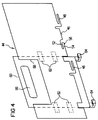
- FIG. 4 In order for the electronic cards 22 to come into contact with one another prevent is between two slots one in figure 1 only indicated partition 44 arranged in Figure 4 is shown in more detail. It essentially consists of a rectangular plastic plate attached to its the Protection plate 32 facing lower edge 46 two hooks 48 has to engage in slot-shaped openings 50 in the Protection plate 32 are determined. Furthermore, at the bottom Edge 46 of the intermediate wall 44 through an incision 52 a Spring tongue 54 formed with a downward facing Latch 56 is provided. The intermediate wall 44 is with the Hook 48 inserted into the openings 50 of the protective plate 32 and then shifted parallel to itself until engage the hooks 48 under the material of the protective plate 32. The latch 56 latches in an opening 58 in the protective plate 32 and thus holds the intermediate wall 44 firmly in their suspended position.
- a pull-out aid in the form of a pull plate 60 slidably mounted in the area of the intermediate wall 44, which after assembly the same on the protective plate 32 between the openings 36 comes to rest in the protective plate 32 is on the intermediate wall 44 a pull-out aid in the form of a pull plate 60 slidably mounted.
- the pull plate is with the help of tabs 62 on the intermediate wall 44 parallel to this led and carries two pull hooks on its lower edge 64, on both sides of the respective plug 24 under the edge of the electronic card facing the protective plate 32 22 grab.
- the pull-out plate 60 has near her upper edge of a handle opening 66, one in this area provided rectangular recess 68 in the intermediate wall 44 makes it easier to grasp the pull-out plate 60.
- each rectangular Openings 70 are formed, into which the pulling hooks 64 are inserted can.
- the pulling hooks 64 pass through the openings 70, reach under the electronics card 22 on both sides of the connector 24 and pull the card 22 with the connector 24 without tilting up. It is sufficient to remove the connector 24 from the mating connector 20 to highlight. Then the electronics card 22 effortlessly between the adjacent partitions be lifted out without the risk of touching or even damage the electronic card or its Neighbor cards exist.
- Figure 2 also shows that also with the protective plate 32 connected side protection wall 40 a pull-out aid 60 stored in the same manner as on the partition walls 44 is.
Landscapes
- Engineering & Computer Science (AREA)
- General Engineering & Computer Science (AREA)
- Theoretical Computer Science (AREA)
- Microelectronics & Electronic Packaging (AREA)
- Computer Hardware Design (AREA)
- Physics & Mathematics (AREA)
- General Physics & Mathematics (AREA)
- Mounting Of Printed Circuit Boards And The Like (AREA)
Description
- Figur 1
- eine schematische perspektivische Teildarstellung eines Gerätechassis zur Aufnahme einer Hauptplatine und einer Mehrzahl von auf diese aufsteckbaren Elektronikkarten,
- Figur 2
- eine Draufsicht auf eine Schutzplatte und mit ihr verbundene Schutzwände zum Abdecken der Hauptplatine und der seitlichen Chassiswände,
- Figur 3
- eine Endansicht der in Figur 2 dargestellten Schutzanordnung und
- Figur 4
- eine perspektivische Darstellung einer Zwischenwand.
Claims (8)
- Chassis zur Aufnahme von Elektronikkarten (22), die parallel zueinander und in einem Abstand voneinander über jeweils mindestens einen Steckverbinder (24) auf eine Gegenstecker (20) tragende und senkrecht zu den Elektronikkarten (22) gerichtete Steckwand (18) aufsteckbar sind, dadurch gekennzeichnet, daß zwischen je zwei Elektronikkarten (22) eine aus einem Isoliermaterial bestehende Zwischenwand (44) angeordnet ist, die an der Steckwand (18) oder an einer aus Isoliermaterial bestehenden, die Steckwand abdeckenden, Durchtrittsöffnungen für die Steckverbinder (24) aufweisenden Schutzplatte (32) befestigt ist.
- Chassis nach Anspruch 1, dadurch gekennzeichnet, daß die Zwischenwände (44) an ihrem jeweiligen der Steckwand (18) zugekehrten Rand (46) mindestens einen Haken (48) haben, der zum Eingriff in eine in der Steckwand (18) oder der Schutzplatte (32) ausgebildete komplementäre Öffnung (50) bestimmt ist.
- Chassis nach Anspruch 1 oder 2, dadurch gekennzeichnet, daß die Zwischenwände (44) durch eine Rastverriegelung (56, 58) an der Steckwand (18) oder der Schutzplatte (32) gesichert sind.
- Chassis nach einem der vorhergehenden Ansprüche, dadurch gekennzeichnet, daß an jeder Zwischenwand (44) ein senkrecht zur Steckwand (18) verstellbares Zugelement (60) verschiebbar gelagert ist, das mit mindestens einem Haken (64) an seinem der Steckwand (18) zugekehrten Ende den der Steckwand (18) zugekehrten Rand einer der zwischenwand benachbarten Elektronikkarte (22) untergreift.
- Chassis nach Anspruch 4, dadurch gekennzeichnet, daß das Zugelement (60) plattenförmig ausgebildet ist und nahe seinem der Steckwand fernen Ende eine Grifföffnung (66) hat.
- Chassis nach Anspruch 4 oder 5, dadurch gekennzeichnet, daß die Schutzplatte (32) oder die Steckwand (18) in Flucht mit dem Haken (64) an dem Zugelement (60) jeweils eine Öffnung (70) hat, in die der Haken (64) bei eingesteckter Elektronikkarte (62) eintauchen kann.
- Chassis nach einem der vorhergehenden Ansprüche, dadurch gekennzeichnet, daß die Schutzplatte (32) an ihren zu den Elektronikkarten (22) parallelen Rändern mit die Chassiswände abdeckenden Schutzwänden (40, 42) verbunden ist.
- Chassis nach Anspruch 7, dadurch gekennzeichnet, daß die Schutzplatte (32), die Schutzwände (40, 42) und die Zwischenwände (44) aus einem transparenten Kunststoff hergestellt sind.
Applications Claiming Priority (3)
| Application Number | Priority Date | Filing Date | Title |
|---|---|---|---|
| DE19806025 | 1998-02-13 | ||
| DE19806025A DE19806025C1 (de) | 1998-02-13 | 1998-02-13 | Chassis zur Aufnahme von Elektronikkarten |
| PCT/DE1999/000323 WO1999041655A1 (de) | 1998-02-13 | 1999-02-05 | Chassis zur aufnahme von elektronikkarten |
Publications (2)
| Publication Number | Publication Date |
|---|---|
| EP1060444A1 EP1060444A1 (de) | 2000-12-20 |
| EP1060444B1 true EP1060444B1 (de) | 2002-05-15 |
Family
ID=7857685
Family Applications (1)
| Application Number | Title | Priority Date | Filing Date |
|---|---|---|---|
| EP99911585A Expired - Lifetime EP1060444B1 (de) | 1998-02-13 | 1999-02-05 | Chassis zur aufnahme von elektronikkarten |
Country Status (3)
| Country | Link |
|---|---|
| EP (1) | EP1060444B1 (de) |
| DE (2) | DE19806025C1 (de) |
| WO (1) | WO1999041655A1 (de) |
Families Citing this family (1)
| Publication number | Priority date | Publication date | Assignee | Title |
|---|---|---|---|---|
| DE10060620C2 (de) * | 2000-12-06 | 2003-02-13 | Jumptec Ind Computertechnik Ag | Einsteckplatine |
Family Cites Families (4)
| Publication number | Priority date | Publication date | Assignee | Title |
|---|---|---|---|---|
| DE3744603C1 (en) * | 1987-12-31 | 1988-10-06 | Kirsten Elektrotech | Centralised electric system for motor vehicles |
| JP2880850B2 (ja) * | 1992-05-07 | 1999-04-12 | 日本電気株式会社 | 導電性構造物の絶縁構造 |
| US5564930A (en) * | 1994-11-14 | 1996-10-15 | Yu; Ben H. | Modular computer case |
| US5754406A (en) * | 1996-06-04 | 1998-05-19 | Compaq Computer Corp. | Printed circuit board card guide having isolation arms and means for securing PCB |
-
1998
- 1998-02-13 DE DE19806025A patent/DE19806025C1/de not_active Expired - Fee Related
-
1999
- 1999-02-05 WO PCT/DE1999/000323 patent/WO1999041655A1/de not_active Ceased
- 1999-02-05 DE DE59901449T patent/DE59901449D1/de not_active Expired - Lifetime
- 1999-02-05 EP EP99911585A patent/EP1060444B1/de not_active Expired - Lifetime
Also Published As
| Publication number | Publication date |
|---|---|
| WO1999041655A1 (de) | 1999-08-19 |
| EP1060444A1 (de) | 2000-12-20 |
| DE59901449D1 (de) | 2002-06-20 |
| DE19806025C1 (de) | 1999-07-15 |
Similar Documents
| Publication | Publication Date | Title |
|---|---|---|
| DE69722055T2 (de) | Elektrischer Verbinder | |
| DE69121270T2 (de) | Zweiteilige Buchseneinheit für modularen Steckeraufbau | |
| WO1997044864A1 (de) | Verrastung einer steckverbinderpaarung | |
| DE69825667T2 (de) | Verriegelung für Smartcard-Adapter | |
| WO2004010536A1 (de) | Steckverbinder für steckerkabel | |
| DE69815017T2 (de) | Entfernung von Leiterplatten | |
| DE4220184C2 (de) | Fernsehgerät mit integriertem Videogerät | |
| DE4102541C1 (de) | ||
| DE69103362T2 (de) | Beförderungsschutz- und Einfügungsgerät für mehradrige Kabel. | |
| DE3621262C2 (de) | Haltevorrichtung für ein elektronisches Display | |
| DE2851749C2 (de) | ||
| EP0669795B1 (de) | Gehäuse zur Aufnahme von bestückten Leiterplatten | |
| DE8630076U1 (de) | Surface-mount-Steckverbinder | |
| DE19806025C1 (de) | Chassis zur Aufnahme von Elektronikkarten | |
| DE19610037C2 (de) | Baugruppenträger | |
| EP0648382B1 (de) | Filter-steckverbinder mit schirmgehäuse | |
| EP0301119B1 (de) | Steckbaugruppe | |
| DE29720511U1 (de) | Einbaugehäuse für Leiterplatten und Elektronikbausteine | |
| DE3626852C2 (de) | ||
| DE19833248A1 (de) | Vorrichtung zum Führen und Massekontaktieren von Leiterplatten | |
| DE102005002138B4 (de) | Gehäuse zur Aufnahme von elektrischen Leiterkarten | |
| EP0755176B1 (de) | Vorrichtung zur Herstellung einer elektrischen und/oder optischen Verbindung | |
| WO1992004688A1 (de) | Kontaktiereinrichtung für eine sim-karte | |
| DE4447372C2 (de) | Handhabungsvorrichtung für eine Einschubeinheit eines elektrischen Gerätes | |
| DE3709041C2 (de) | Vorrichtung zur Verriegelung von in ein Gehäuse eingebrachten Baugruppenträgerplatten |
Legal Events
| Date | Code | Title | Description |
|---|---|---|---|
| PUAI | Public reference made under article 153(3) epc to a published international application that has entered the european phase |
Free format text: ORIGINAL CODE: 0009012 |
|
| 17P | Request for examination filed |
Effective date: 20000525 |
|
| AK | Designated contracting states |
Kind code of ref document: A1 Designated state(s): DE FR GB |
|
| GRAG | Despatch of communication of intention to grant |
Free format text: ORIGINAL CODE: EPIDOS AGRA |
|
| GRAG | Despatch of communication of intention to grant |
Free format text: ORIGINAL CODE: EPIDOS AGRA |
|
| GRAH | Despatch of communication of intention to grant a patent |
Free format text: ORIGINAL CODE: EPIDOS IGRA |
|
| 17Q | First examination report despatched |
Effective date: 20010801 |
|
| GRAH | Despatch of communication of intention to grant a patent |
Free format text: ORIGINAL CODE: EPIDOS IGRA |
|
| GRAA | (expected) grant |
Free format text: ORIGINAL CODE: 0009210 |
|
| AK | Designated contracting states |
Kind code of ref document: B1 Designated state(s): DE FR GB |
|
| REG | Reference to a national code |
Ref country code: GB Ref legal event code: FG4D Free format text: NOT ENGLISH |
|
| REF | Corresponds to: |
Ref document number: 59901449 Country of ref document: DE Date of ref document: 20020620 |
|
| GBT | Gb: translation of ep patent filed (gb section 77(6)(a)/1977) |
Effective date: 20020720 |
|
| ET | Fr: translation filed | ||
| PLBE | No opposition filed within time limit |
Free format text: ORIGINAL CODE: 0009261 |
|
| STAA | Information on the status of an ep patent application or granted ep patent |
Free format text: STATUS: NO OPPOSITION FILED WITHIN TIME LIMIT |
|
| 26N | No opposition filed |
Effective date: 20030218 |
|
| PGFP | Annual fee paid to national office [announced via postgrant information from national office to epo] |
Ref country code: FR Payment date: 20100303 Year of fee payment: 12 |
|
| PGFP | Annual fee paid to national office [announced via postgrant information from national office to epo] |
Ref country code: GB Payment date: 20100224 Year of fee payment: 12 Ref country code: DE Payment date: 20100223 Year of fee payment: 12 |
|
| GBPC | Gb: european patent ceased through non-payment of renewal fee |
Effective date: 20110205 |
|
| REG | Reference to a national code |
Ref country code: FR Ref legal event code: ST Effective date: 20111102 |
|
| PG25 | Lapsed in a contracting state [announced via postgrant information from national office to epo] |
Ref country code: FR Free format text: LAPSE BECAUSE OF NON-PAYMENT OF DUE FEES Effective date: 20110228 |
|
| REG | Reference to a national code |
Ref country code: DE Ref legal event code: R119 Ref document number: 59901449 Country of ref document: DE Effective date: 20110901 |
|
| PG25 | Lapsed in a contracting state [announced via postgrant information from national office to epo] |
Ref country code: GB Free format text: LAPSE BECAUSE OF NON-PAYMENT OF DUE FEES Effective date: 20110205 |
|
| PG25 | Lapsed in a contracting state [announced via postgrant information from national office to epo] |
Ref country code: DE Free format text: LAPSE BECAUSE OF NON-PAYMENT OF DUE FEES Effective date: 20110901 |