EP1056285A2 - Video display apparatus capable of displaying video signals of a plurality of types with different specifications - Google Patents
Video display apparatus capable of displaying video signals of a plurality of types with different specifications Download PDFInfo
- Publication number
- EP1056285A2 EP1056285A2 EP00304328A EP00304328A EP1056285A2 EP 1056285 A2 EP1056285 A2 EP 1056285A2 EP 00304328 A EP00304328 A EP 00304328A EP 00304328 A EP00304328 A EP 00304328A EP 1056285 A2 EP1056285 A2 EP 1056285A2
- Authority
- EP
- European Patent Office
- Prior art keywords
- signal
- video
- format
- driver
- control
- Prior art date
- Legal status (The legal status is an assumption and is not a legal conclusion. Google has not performed a legal analysis and makes no representation as to the accuracy of the status listed.)
- Withdrawn
Links
- 238000006243 chemical reaction Methods 0.000 claims description 10
- 239000011159 matrix material Substances 0.000 claims description 2
- 238000000034 method Methods 0.000 description 26
- 102100040862 Dual specificity protein kinase CLK1 Human genes 0.000 description 14
- 238000003780 insertion Methods 0.000 description 13
- 230000037431 insertion Effects 0.000 description 13
- 238000005070 sampling Methods 0.000 description 12
- 101100191136 Arabidopsis thaliana PCMP-A2 gene Proteins 0.000 description 6
- 101100048260 Saccharomyces cerevisiae (strain ATCC 204508 / S288c) UBX2 gene Proteins 0.000 description 6
- 238000010586 diagram Methods 0.000 description 6
- 230000008707 rearrangement Effects 0.000 description 5
- 230000000630 rising effect Effects 0.000 description 5
- 239000003550 marker Substances 0.000 description 4
- 230000006870 function Effects 0.000 description 2
- 102100040844 Dual specificity protein kinase CLK2 Human genes 0.000 description 1
- 101000749294 Homo sapiens Dual specificity protein kinase CLK1 Proteins 0.000 description 1
- 101000749291 Homo sapiens Dual specificity protein kinase CLK2 Proteins 0.000 description 1
- 238000001514 detection method Methods 0.000 description 1
- 238000009877 rendering Methods 0.000 description 1
Images


Classifications
-
- G—PHYSICS
- G09—EDUCATION; CRYPTOGRAPHY; DISPLAY; ADVERTISING; SEALS
- G09G—ARRANGEMENTS OR CIRCUITS FOR CONTROL OF INDICATING DEVICES USING STATIC MEANS TO PRESENT VARIABLE INFORMATION
- G09G5/00—Control arrangements or circuits for visual indicators common to cathode-ray tube indicators and other visual indicators
- G09G5/003—Details of a display terminal, the details relating to the control arrangement of the display terminal and to the interfaces thereto
- G09G5/006—Details of the interface to the display terminal
- G09G5/008—Clock recovery
-
- G—PHYSICS
- G09—EDUCATION; CRYPTOGRAPHY; DISPLAY; ADVERTISING; SEALS
- G09G—ARRANGEMENTS OR CIRCUITS FOR CONTROL OF INDICATING DEVICES USING STATIC MEANS TO PRESENT VARIABLE INFORMATION
- G09G5/00—Control arrangements or circuits for visual indicators common to cathode-ray tube indicators and other visual indicators
- G09G5/003—Details of a display terminal, the details relating to the control arrangement of the display terminal and to the interfaces thereto
- G09G5/005—Adapting incoming signals to the display format of the display terminal
-
- H—ELECTRICITY
- H04—ELECTRIC COMMUNICATION TECHNIQUE
- H04N—PICTORIAL COMMUNICATION, e.g. TELEVISION
- H04N5/00—Details of television systems
- H04N5/04—Synchronising
- H04N5/12—Devices in which the synchronising signals are only operative if a phase difference occurs between synchronising and synchronised scanning devices, e.g. flywheel synchronising
- H04N5/126—Devices in which the synchronising signals are only operative if a phase difference occurs between synchronising and synchronised scanning devices, e.g. flywheel synchronising whereby the synchronisation signal indirectly commands a frequency generator
-
- H—ELECTRICITY
- H04—ELECTRIC COMMUNICATION TECHNIQUE
- H04N—PICTORIAL COMMUNICATION, e.g. TELEVISION
- H04N5/00—Details of television systems
- H04N5/44—Receiver circuitry for the reception of television signals according to analogue transmission standards
- H04N5/46—Receiver circuitry for the reception of television signals according to analogue transmission standards for receiving on more than one standard at will
-
- G—PHYSICS
- G09—EDUCATION; CRYPTOGRAPHY; DISPLAY; ADVERTISING; SEALS
- G09G—ARRANGEMENTS OR CIRCUITS FOR CONTROL OF INDICATING DEVICES USING STATIC MEANS TO PRESENT VARIABLE INFORMATION
- G09G2340/00—Aspects of display data processing
- G09G2340/04—Changes in size, position or resolution of an image
- G09G2340/0407—Resolution change, inclusive of the use of different resolutions for different screen areas
-
- G—PHYSICS
- G09—EDUCATION; CRYPTOGRAPHY; DISPLAY; ADVERTISING; SEALS
- G09G—ARRANGEMENTS OR CIRCUITS FOR CONTROL OF INDICATING DEVICES USING STATIC MEANS TO PRESENT VARIABLE INFORMATION
- G09G2340/00—Aspects of display data processing
- G09G2340/04—Changes in size, position or resolution of an image
- G09G2340/0442—Handling or displaying different aspect ratios, or changing the aspect ratio
-
- G—PHYSICS
- G09—EDUCATION; CRYPTOGRAPHY; DISPLAY; ADVERTISING; SEALS
- G09G—ARRANGEMENTS OR CIRCUITS FOR CONTROL OF INDICATING DEVICES USING STATIC MEANS TO PRESENT VARIABLE INFORMATION
- G09G3/00—Control arrangements or circuits, of interest only in connection with visual indicators other than cathode-ray tubes
- G09G3/20—Control arrangements or circuits, of interest only in connection with visual indicators other than cathode-ray tubes for presentation of an assembly of a number of characters, e.g. a page, by composing the assembly by combination of individual elements arranged in a matrix no fixed position being assigned to or needed to be assigned to the individual characters or partial characters
- G09G3/34—Control arrangements or circuits, of interest only in connection with visual indicators other than cathode-ray tubes for presentation of an assembly of a number of characters, e.g. a page, by composing the assembly by combination of individual elements arranged in a matrix no fixed position being assigned to or needed to be assigned to the individual characters or partial characters by control of light from an independent source
- G09G3/36—Control arrangements or circuits, of interest only in connection with visual indicators other than cathode-ray tubes for presentation of an assembly of a number of characters, e.g. a page, by composing the assembly by combination of individual elements arranged in a matrix no fixed position being assigned to or needed to be assigned to the individual characters or partial characters by control of light from an independent source using liquid crystals
- G09G3/3611—Control of matrices with row and column drivers
- G09G3/3648—Control of matrices with row and column drivers using an active matrix
-
- G—PHYSICS
- G09—EDUCATION; CRYPTOGRAPHY; DISPLAY; ADVERTISING; SEALS
- G09G—ARRANGEMENTS OR CIRCUITS FOR CONTROL OF INDICATING DEVICES USING STATIC MEANS TO PRESENT VARIABLE INFORMATION
- G09G5/00—Control arrangements or circuits for visual indicators common to cathode-ray tube indicators and other visual indicators
- G09G5/003—Details of a display terminal, the details relating to the control arrangement of the display terminal and to the interfaces thereto
- G09G5/006—Details of the interface to the display terminal
Definitions
- the present invention relates to a video display apparatus such as an LCD. More particularly, the present invention relates to a video display apparatus capable of displaying video signals of a plurality of types having different specifications.
- the latter method on the other hand, an input picture signal is subjected to signal processing such as IP conversion and format conversion. For this reason, the latter method is flexible in that it can be applied to not only a CRT but also a plane display unit such as an LCD and a PDP.
- the latter method requires a memory with a large capacity for signal processing such as interlaced-scanning/sequential-scanning conversion, frame-rate conversion and picture-size shrinkage/enlargement conversion.
- the method described above has a problem of a higher cost and increased power consumption due to a need for a memory with a large size.
- the present invention provides a video display apparatus for displaying an input video signal as video information in a display format different from a format of the input video signal on a display panel with a plurality of pixels laid out thereon to form a matrix.
- the video display apparatus comprises: a video-signal processing circuit for converting the input video signal into a digital signal and processing the digital signal obtained as a result of conversion; a PLL circuit for generating a clock signal for the video-signal processing circuit; a discrimination means for identifying a format of the input video signal from the input video signal; a specification means for specifying a format of video information to be displayed on the display panel; a driver-control-signal generation means for generating control signals for controlling a gate driver for driving the display panel and control signals for controlling a source driver also for driving the display panel in accordance with a format of video information to be displayed on the display panel; a driver-control-signal switching means for selecting one of the control signals generated by the driver-control-signal generation means for controlling the gate driver and
- a particular control signal generated by the driver-control-signal generation means for controlling the gate driver and a particular control signal generated by the driver-control-signal generation means for controlling the source driver are selected in accordance with a format of the input video signal identified by the discrimination means and a display format specified by the specification means.
- the video-signal processing circuit carries out processing with the clock signal from the PLL circuit controlled by the PLL-signal control means in accordance with a format of the input video signal identified by the discrimination means and a display format specified by the specification means.
- the discrimination means identifies a format of the input video signal from an aspect ratio of the input video signal and the number of scan lines of the input video signal.
- the discrimination means is capable of identifying a format of the input video signal from a synchronization signal of the input video signal.
- the video display apparatus is desirable in that the circuit configuration of the discrimination means is simple.
- the discrimination means is capable of determining whether the input video signal is a signal of an NTSC system, a signal of a PAL system or a signal of an HDTV system only from the number of scan lines in the vertical period.
- the specification means specifies a format of video information to be displayed on the display panel from an aspect ratio of the input video signal or the number of scan lines of the input video signal.
- This method of specification is particularly effective for a case in which the only difference between the display format and the format of the input video signal is the aspect ratio or the number of scan lines.
- the video-signal processing circuit carries out processing based on a clock signal having a first frequency for a video period of the digital signal and a frequency for periods other than the video period different from the first frequency.
- the video display apparatus is desirable in that all pixels of the display panel can be displayed within a limited period of time in case the number of effective display pixels in the input video signal is smaller than the number of pixels on the display panel.
- the source driver for driving the display panel is driven by a clock signal having a first frequency for a video period of the digital signal and a frequency for periods other than the video period different from the first frequency.
- the video display apparatus is desirable in that all pixels of the display panel can be displayed within a limited period of time in case the number of effective display pixels in the input video signal is smaller than the number of pixels on the display panel.
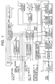
- a horizontal synchronization signal HD and a vertical synchronization signal VD are supplied to an automatic discrimination circuit 1.
- the automatic discrimination circuit 1 is a circuit for automatically determining whether a video signal supplied to the video display apparatus is an NTSC or PAL signal.
- An automatic discrimination signal AD output by the automatic discrimination circuit 1 is supplied to a PLL-control-signal generation circuit 2, a TFT-LCD driver control circuit 3 and a frequency-division switching circuit 7.
- the PLL-control-signal generation circuit 2 and the TFT-LCD driver control circuit 3 also receive a 4:3/16:9 switching signal K1, a normal/enlargement switching signal K2, an HDTV switching signal K3 and a 1080/1035 switching signal K4.
- the horizontal synchronization signal HD, the vertical synchronization signal VD and a clock signal CLK are supplied to the PLL-control-signal generation circuit 2 which outputs a control signal CNT to a PLL circuit 4.
- the PLL circuit 4 generates the clock signal CLK.
- the horizontal synchronization signal HD and the vertical synchronization signal VD are also supplied to a V counter 5 which outputs a signal to the TFT-LCD driver control circuit 3.
- the horizontal synchronization signal HD and the clock signal CLK are supplied to an H counter 6 which also outputs a signal to the TFT-LCD driver control circuit 3. It should be noted that the clock signal CLK is also supplied directly to the TFT-LCD driver control circuit 3.
- the clock signal CLK, the switching signals K1 to K4 and the automatic discrimination signal AD are supplied to the frequency-division switching circuit 7 which outputs a driver clock signal to a source driver 8.
- a signal output by the TFT-LCD driver control circuit 3 is supplied to the source driver 8 and a gate driver 9. Signals output by the source driver 8 and the gate driver 9 are supplied to a TFT-LCD 10.
- a video signal input to the video display apparatus is supplied to a video-signal processing circuit 21.
- Embedded in the video-signal processing circuit 21 are an A/D conversion circuit 22, a peaking circuit 11, a blanking-marker insertion circuit 12, a margin insertion circuit 13, a tally and indicator insertion circuit 14 and a video-data rearrangement circuit 15.
- the video signal supplied to the video-signal processing circuit 21 is fed to the A/D conversion circuit 22 which outputs a signal to the peaking circuit 11.
- a signal generated by the peaking circuit 11 is supplied to the blanking-marker insertion circuit 12 which outputs a signal to the margin insertion circuit 13.
- a signal output by the margin insertion circuit 13 is supplied to the tally and indicator insertion circuit 14 which outputs a signal to the video-data rearrangement circuit 15.
- a signal generated by the video-data rearrangement circuit 15 is the output of the video-signal processing circuit 21 which is supplied to the source driver 8.
- a first output CLK1 of the frequency-division switching circuit 7 is supplied to the peaking circuit 11 whereas a second output CLK2 of the frequency-division switching circuit 7 is supplied to the peaking circuit 11, the blanking-marker insertion circuit 12, the margin insertion circuit 13, the tally and indicator insertion circuit 14 and the video-data rearrangement circuit 15.
- a signal output by the TFT-LCD driver control circuit 3 is supplied to the blanking-marker insertion circuit 12, the margin insertion circuit 13, the tally and indicator insertion circuit 14 and the video-data rearrangement circuit 15.
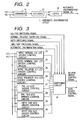
- the internal configuration of the automatic discrimination circuit 1 is explained by referring to Fig. 2.
- Embedded in the automatic discrimination circuit 1 are a counter 16, a decoder 17 and a latch 18 as shown in the figure.
- the horizontal synchronization signal HD and the vertical synchronization signal VD input to the automatic discrimination circuit 1 are supplied to the counter 16.
- the vertical synchronization signal VD is also supplied to the latch 18 as well.
- a signal output by the counter 16 is supplied to the decoder 17 which outputs a signal to the latch 18.
- the latch 18 generates an automatic discrimination signal AD.
- the automatic discrimination signal AD is output to components external to the automatic discrimination circuit 1.
- the automatic discrimination signal AD is supplied to the PLL-control-signal generation circuit 2, the TFT-LCD driver control circuit 3 and the frequency-division switching circuit 7.
- the TFT-LCD driver control circuit 3 comprises embedded components including an NTSC normal 4:3 LCD driver control circuit 23, an NTSC normal 16:9 LCD driver control circuit 24, an NTSC enlarge 4:3 LCD driver control circuit 25, an NTSC enlargel6:9 LCD driver control circuit 26, a PAL 4:3 LCD driver control circuit 27, a PAL 16:9 LCD driver control circuit 28, an HDTV 1080 LCD driver control circuit 29, an HDTV 1035 LCD driver control circuit 30 and a switching circuit 31.
- An output V_C of the V counter 5 and an output H_C of the H counter 6 are supplied to the LCD driver control circuits 23 to 30 which each output a signal to the switching circuit 31.
- the switching circuit 31 also receives the 4:3/16:9 switching signal K1, the normal/enlargement switching signal K2, the HDTV switching signal K3, the 1080/1035 switching signal K4 and the automatic discrimination signal AD.
- the switching circuit 31 outputs a source driver control signal and a gate driver control signal to the source driver 8 and the gate driver 9 respectively.
- the automatic discrimination circuit 1 In order to determine whether a signal supplied to the video display apparatus is an NTSC or PAL signal, the automatic discrimination circuit 1 counts the number of times the horizontal synchronization signal HD goes from a high level to a low level during 1 V period which is defined as a period between a rising edge of the vertical synchronization signal VD and a falling edge following the rising edge.
- the decoder 17 On the falling edge of the vertical synchronization signal VD supplied to the counter 16, the counter 16 is reset. After being reset, the counter 16 starts counting the number of times the horizontal synchronization signal HD supplied to the counter 16 goes from a high level to a low level. A falling-edge count obtained as a result of the counting is supplied to the decoder 17 to be decoded. For example, the decoder 17 outputs a signal at a low level when the falling-edge count output by the counter 16 becomes equal to 1 and outputs a signal at a high level when the falling-edge count becomes equal to 310. The signal output by the decoder is supplied to the latch 18 which latches the signal on the falling edge of the vertical synchronization signal VD.
- An NTSC signal supplied to the video display apparatus is an interlace signal.
- the signal output by the decoder 17 is reset at the low level which is latched in the latch 18 on the next falling edge of the vertical synchronization signal VD.
- the automatic discrimination signal AD generated by the latch 18 is also reset at the low level as well.
- the number of times the horizontal synchronization signal HD goes from a high level to a low level during 1 V period is about half the sum of the number of scan lines in a video period (575) and the number of scan lines in a blanking period, that is, about 320.
- the signal output by the decoder 17 is set at the high level which is latched in the latch 18 on the next falling edge of the vertical synchronization signal VD.
- the automatic discrimination signal AD generated by the latch 18 is also reset at the high level as well.
- the PLL-control-signal generation circuit 2 detects how many clocks are counted in an H period (1 horizontal period) and determines the frequency of the clock signal CLK output by the PLL circuit 4 on the basis of the result of the detection.
- the TFT-LCD 10 has 960 pixels in the horizontal direction and 540 pixels in the vertical direction. If a picture with a pixel count different from the TFT-LCD 10 or an aspect ratio different from the TFT-LCD 10 is displayed on this screen, a margin area with none displayed thereon is resulted in on the screen.
- Types of a video signal supplied to the video display apparatus include NTSC, PAL and HDTV. Furthermore, the HDTV type may have a scan line count of 1,080 or 1,035.
- display selections include a technique of displaying the input picture as it is (or a normal display method) and a technique of displaying an enlarged picture (or an enlarged display method).
- display selections include a display technique with an aspect ratio of 4 : 3 unchanged as it is and a display technique adopting an aspect ratio of 16 : 9.
- Fig. 4 is a table showing the number of pixels, the number of actual scan lines, a scan line change method, a clock frequency and a clock division ratio for each combination of the type of an input signal and a display technique.
- the combinations include NTSC normal 4 : 3, NTSC normal 16 : 9, NTSC enlarge 4 : 3, NTSC enlarge 16 : 9, PAL 4 : 3, PAL 16 : 9, HDTV 1080 and HDTV 1035.
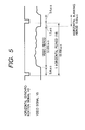
- Fig. 5 is a diagram showing a relation between the horizontal synchronization signal HD and the vertical synchronization signal VD for the NTSC system.
- the period of the clock signal CLK is set at 27.13 ns and this clock signal CLK is used for sampling the margin area or used during the horizontal blanking period as it is.
- the period of the clock signal CLK is set by the PLL-control-signal generation circuit 2.
- a method of displaying a margin area for the NTSC normal 16 : 9 display system is explained as follows.
- the frequency can be changed by the PLL circuit 4. In general, however, if a wide variable-frequency range of the clock signal CLK output by the PLL circuit 4 is used, the stability of the PLL circuit 4 deteriorates.
- the frequency of the clock signal for the NTSC normal 16 : 9 display system is set at 32.74 MHz which is twice the frequency of 16.37 MHz. At this frequency of 32.74 MHz, 1 pixel is sampled by 2 clock pulses.
- the number of effective scan lines in the vertical direction is 1,080 which is greater than 540, the number of pixels in the vertical direction on the screen of the TFT-LCD 10.
- odd fields and even fields are superposed on each other in the so-called thinning process to reduce the number of effective scan lines in the vertical direction to 540.
- the sampling period in 1 horizontal period according to HDTV specifications is 25.86 ⁇ s
- This frequency is about the same as that of the NTSC normal 4 : 3 display system.
- the frequency of 37.125 MHz is used as it is without carrying out frequency division.
- sampling clock frequencies for the NTSC enlarge 4:3, NTSC enlarge 16 : 9, PAL 4 : 3, PAL 16 : 9 and HDTV 1035 display systems can be determined.
- the sampling clock frequencies for the display systems are shown in Fig. 5.
- the V counter 5 counts the number of HD pulses in 1 V period and the H counter 6 counts the number of rising CLK pulses in 1 H period.
- the V counter 5 and the H counter 6 control the TFT-LCD driver control circuit 3 on the basis of numbers obtained as results of counting by the V counter 5 and the H counter 6.
- An output V_C of the V counter 5 and an output H_C of the H counter 6 are supplied to the LCD driver control circuits 23 to 30 which each output a driver control signal according to the respective display format to the switching circuit 31.
- the switching circuit 31 selects and outputs only a desired driver control signal.
- the selection of the driver control signal by the switching circuit 31 is based on the 4:3/16:9 switching signal K1, the normal/enlargement switching signal K2, the HDTV switching signal K3, the 1080/1035 switching signal K4 and the automatic discrimination signal AD.
- the output of the switching circuit 31 is split into a source driver control signal and a gate driver control signal which are supplied to the source driver 8 and the gate driver 9 respectively.
- the TFT-LCD driver control circuit 3 outputs a start pulse to the source driver 8 typically in order to determine a display start position in the horizontal direction.
- the source driver 8 then starts rendering the margin area at the time the start pulse in one horizontal period is received.
- the LCD driver control circuits 23 to 30 embedded in the TFT-LCD driver control circuit 3 generate start pulses for all the respective display systems.
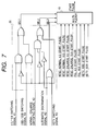
- One of the start pulses that matches the display format is selected by a multiplexer 19 embedded in the switching circuit 31.
- the multiplexer 19 is shown in Fig. 7.
- the selected start pulse is supplied to the source driver 8 as a source driver control signal.
- a gate circuit 20 shown in Fig. 7 is also embedded in the switching circuit 31. As shown in the figure, the gate circuit 20 receives the switching signal K1 to K4 and the automatic discrimination signal AD, and the switching signal K1 to K4 and the automatic discrimination signal AD are converted into multiplexer control select signals SEL1 to SEL3 which are supplied to the multiplexer 19.
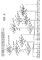
- the multiplexer control select signals SEL1 to SEL3 control the multiplexer 19 to carry out switching operations in accordance with a flowchart shown in Fig. 6. To be more specific, the multiplexer 19 selects one of input start pulses with a plurality of types in accordance with the multiplexer control select signals SEL1 to SEL3 received from the gate circuit 20.
- a relation between the multiplexer control select signals SEL1 to SEL3 and start pulses to be selected in accordance with the multiplexer control select signals SEL1 to SEL3 is shown in Fig. 8.
- a pulse signal selected by the switching circuit 31 is used for generating control signals supplied to the source driver 8 and the gate driver 9.
- the switching signal K1 to K4 are also supplied to the PLL-control-signal generation circuit 2 which outputs a PLL control signal CNT to the PLL circuit 4.
- the PLL control signal CNT is changed in dependence on the switching signal K1 to K4 so that the frequency of a clock signal CLK generated by the PLL circuit 4 is also changed in dependence on the switching signal K1 to K4.
- the flowchart begins with a step S1 at which the level of the automatic discrimination signal AD output by the automatic discrimination circuit 1 is examined.
- An automatic discrimination signal AD set at a high level indicates that the video signal supplied to the video display apparatus is a PAL or HDTV signal. In this case, the flow of the processing goes on to a step S2.
- an automatic discrimination signal AD reset at a low level indicates that the video signal supplied to the video display apparatus is an NTSC or HDTV signal. In this case, the flow of the processing goes on to a step S5.
- the level of the HDTV switching signal K3 is examined. If the HDTV switching signal K3 is found set to the high level, that is, if the video signal supplied to the video display apparatus is an HDTV signal, the flow of the processing goes on to a step S3. If the HDTV switching signal K3 is found reset at the low level, that is, if the video signal supplied to the video display apparatus is a PAL signal, on the other hand, the flow of the processing goes on to a step S4.
- the level of the 1080/1035 switching signal K4 is examined. If the 1080/1035 switching signal K4 is found set to the high level, that is, if the video signal supplied to the video display apparatus is an HDTV 1035 signal, the display system is switched to HDTV 1035. If the 1080/1035 switching signal K4 is found reset at the low level, that is, if the video signal supplied to the video display apparatus is a HDTV 1080 signal, on the other hand, the display system is switched to HDTV 1080.
- the level of the 4:3/16:9 switching signal K1 is examined. If the 4:3/16:9 switching signal K1 is found set to the high level, that is, if the video signal supplied to the video display apparatus is a PAL signal with an aspect ratio of 16 : 9, the display system is switched to PAL with an aspect ratio of 16 : 9. If the 4:3/16:9 switching signal K1 is found reset at the low level, that is, if the video signal supplied to the video display apparatus is a PAL signal with an aspect ratio of 4 : 3, on the other hand, the display system is switched to PAL signal with an aspect ratio of 4 : 3.
- the level of the HDTV switching signal K3 is examined. If the HDTV switching signal K3 is found set to the high level, that is, if the video signal supplied to the video display apparatus is an HDTV signal, the flow of the processing goes on to a step S6. If the HDTV switching signal K3 is found reset at the low level, that is, if the video signal supplied to the video display apparatus is an NTSC signal, on the other hand, the flow of the processing goes on to a step S7.
- the level of the 1080/1035 switching signal K4 is examined. If the 1080/1035 switching signal K4 is found set to the high level, that is, if the video signal supplied to the video display apparatus is an HDTV 1035 signal, the display system is switched to HDTV 1035. If the 1080/1035 switching signal K4 is found reset at the low level, that is, if the video signal supplied to the video display apparatus is a HDTV 1080 signal, on the other hand, the display system is switched to HDTV 1080.
- the level of the 4:3/16:9 switching signal K1 is examined. If the 4:3/16:9 switching signal K1 is found set to the high level, that is, if the video signal supplied to the video display apparatus is an NTSC signal with an aspect ratio of 16 : 9, the flow of the processing goes on to a step S8. If the 4:3/16:9 switching signal K1 is found reset at the low level, that is, if the video signal supplied to the video display apparatus is an NTSC signal an aspect ratio of 4 ; 3, on the other hand, the flow of the processing goes on to a step S9.
- the level of the normal/enlargement switching signal K2 is examined. If the normal/enlargement switching signal K2 is found set to the high level, that is, if the NTSC video signal supplied to the video display apparatus with an aspect ratio of 16 : 9 is to be output as an enlarged display, the display system is switched to HDTV enlarged 16 : 9. If the normal/enlargement switching signal K2 is found reset at the low level, that is, if the NTSC video signal supplied to the video display apparatus with an aspect ratio of 16 : 9 is not to be enlarged but to be output as a normal display, on the other hand, the display system is switched to HDTV normal 16 : 9.
- the level of the normal/enlargement switching signal K2 is examined. If the normal/enlargement switching signal K2 is found set to the high level, that is, if the NTSC video signal supplied to the video display apparatus with an aspect ratio of 4 : 3 is to be output as an enlarged display, the display system is switched to HDTV enlarged 4 : 3. If the normal/enlargement switching signal K2 is found reset at the low level, that is, if the NTSC video signal supplied to the video display apparatus with an aspect ratio of 4 : 3 is not to be enlarged but to be output as a normal display, on the other hand, the display system is switched to HDTV normal 4 : 3.
- the present invention it is possible to display video information with a variety of formats on a video display apparatus without using a memory with a large size. As a result, the cost and the power consumption of the apparatus can be suppressed.
Landscapes
- Engineering & Computer Science (AREA)
- Physics & Mathematics (AREA)
- Computer Hardware Design (AREA)
- General Physics & Mathematics (AREA)
- Theoretical Computer Science (AREA)
- Multimedia (AREA)
- Signal Processing (AREA)
- Transforming Electric Information Into Light Information (AREA)
- Liquid Crystal Display Device Control (AREA)
- Control Of Indicators Other Than Cathode Ray Tubes (AREA)
- Controls And Circuits For Display Device (AREA)
Abstract
Description
Claims (6)
- A video display apparatus for displaying an input video signal as video information in a display format different from a format of the input video signal on a display panel with a plurality of pixels laid out thereon to form a matrix, the video display apparatus comprising:a video-signal processing circuit for converting the input video signal into a digital signal and processing the digital signal obtained as a result of conversion;a PLL circuit for generating a clock signal for the video-signal processing circuit;discrimination means for identifying a format of the input video signal from the input video signal;specification means for specifying a format of video information to be displayed on the display panel;driver-control-signal generation means for generating control signals for controlling a gate driver for driving the display panel and control signals for controlling a source driver also for driving the display panel in accordance with a format of video information to be displayed on the display panel;driver-control-signal switching means for selecting one of the control signals generated by the driver-control-signal generation means for controlling the gate driver and selecting one of the control signals generated by the driver-control-signal generation means for controlling the source driver in accordance with a format of the input video signal identified by the discrimination means and a display format specified by the specification means; andPLL-signal control means for controlling the clock signal generated by the PLL circuit in accordance with a format of the input video signal identified by the discrimination means and a display format specified by the specification means.
- A video display apparatus according to claim 1, wherein the discrimination means identifies a format of the input video signal from an aspect ratio of the input video signal and the number of scan lines of the input video signal.
- A video display apparatus according to claim 2, wherein the discrimination means determines whether the input video signal is a signal of an NTSC system, a signal of a PAL system or a signal of an HDTV system.
- A video display apparatus according to claim 1, wherein the specification means specifies a format of video information to be displayed on the display panel from an aspect ratio of the input video signal or the number of scan lines of the input video signal.
- A video display apparatus according to claim 1, wherein the video-signal processing circuit carries out processing based on a clock signal having a first frequency for a video period of the digital signal and a frequency for periods other than the video period different from the first frequency.
- A video display apparatus according to claim 1, wherein the source driver for driving the display panel is driven by a clock signal having a first frequency for a video period of the digital signal and a frequency for periods other than the video period different from the first frequency.
Applications Claiming Priority (2)
| Application Number | Priority Date | Filing Date | Title |
|---|---|---|---|
| JP11150727A JP2000338925A (en) | 1999-05-28 | 1999-05-28 | Video display device |
| JP15072799 | 1999-05-28 |
Publications (2)
| Publication Number | Publication Date |
|---|---|
| EP1056285A2 true EP1056285A2 (en) | 2000-11-29 |
| EP1056285A3 EP1056285A3 (en) | 2003-09-17 |
Family
ID=15503102
Family Applications (1)
| Application Number | Title | Priority Date | Filing Date |
|---|---|---|---|
| EP00304328A Withdrawn EP1056285A3 (en) | 1999-05-28 | 2000-05-23 | Video display apparatus capable of displaying video signals of a plurality of types with different specifications |
Country Status (5)
| Country | Link |
|---|---|
| US (1) | US6384867B1 (en) |
| EP (1) | EP1056285A3 (en) |
| JP (1) | JP2000338925A (en) |
| KR (1) | KR100339898B1 (en) |
| TW (1) | TW465240B (en) |
Cited By (2)
| Publication number | Priority date | Publication date | Assignee | Title |
|---|---|---|---|---|
| EP1315139A3 (en) * | 2001-11-12 | 2006-01-11 | Samsung SDI Co., Ltd. | Image display method and system for plasma display panel |
| WO2008099948A1 (en) * | 2007-02-08 | 2008-08-21 | Nec Display Solutions, Ltd. | Image display apparatus and frequency adjustment method thereof |
Families Citing this family (27)
| Publication number | Priority date | Publication date | Assignee | Title |
|---|---|---|---|---|
| US6331862B1 (en) * | 1988-07-06 | 2001-12-18 | Lg Philips Lcd Co., Ltd. | Image expansion display and driver |
| KR100281885B1 (en) * | 1998-12-28 | 2001-02-15 | 윤종용 | Clock frequency converter of digital signal receiver |
| JP4144193B2 (en) * | 2000-10-25 | 2008-09-03 | ソニー株式会社 | Display panel and display device |
| JP2003288065A (en) | 2002-03-28 | 2003-10-10 | Seiko Epson Corp | Image display device |
| JP3796751B2 (en) * | 2002-05-02 | 2006-07-12 | ソニー株式会社 | Video signal processing apparatus and method, recording medium, and program |
| CN100435564C (en) * | 2003-05-28 | 2008-11-19 | 松下电器产业株式会社 | Digital interface decoding receiving device |
| KR100949435B1 (en) | 2003-06-24 | 2010-03-25 | 엘지디스플레이 주식회사 | Driving device and driving method of liquid crystal display |
| US20050030386A1 (en) * | 2003-08-04 | 2005-02-10 | John Kamieniecki | Method and apparatus for determining video formats supported by a digital television receiver |
| US6972803B2 (en) * | 2003-09-10 | 2005-12-06 | Gennum Corporation | Video signal format detector and generator system and method |
| US7432991B1 (en) * | 2003-10-01 | 2008-10-07 | Darwin Chang | Random access display monitor |
| US20050094030A1 (en) * | 2003-11-03 | 2005-05-05 | Lsi Logic Corporation | Method and/or circuitry for video frame rate and/or size conversion |
| US7830348B2 (en) * | 2003-12-11 | 2010-11-09 | Au Optronics Corporation | Integrated circuit for liquid crystal display device |
| JP4560445B2 (en) | 2004-06-30 | 2010-10-13 | キヤノン株式会社 | Display device and driving method |
| JP2006171342A (en) * | 2004-12-15 | 2006-06-29 | Sharp Corp | Liquid crystal display |
| JP2006184619A (en) * | 2004-12-28 | 2006-07-13 | Sharp Corp | Video display device |
| JP2006333000A (en) * | 2005-05-25 | 2006-12-07 | Sharp Corp | Video display device |
| KR100747499B1 (en) * | 2005-07-26 | 2007-08-08 | 삼성전자주식회사 | Image processing apparatus and image processing method |
| US7532252B2 (en) * | 2005-09-20 | 2009-05-12 | National Semiconductor Corporation | Video mode detection circuit |
| DE102005048826B3 (en) * | 2005-10-10 | 2007-04-12 | Infineon Technologies Ag | Semiconductor component has pretensioned double-sided adhesive foil between back of semiconductor chip and chip connecting surface with circuit carrier to separate into individual areas without tools |
| JP5056211B2 (en) | 2007-06-29 | 2012-10-24 | ソニー株式会社 | Video signal conversion device, video signal conversion method, and video display device |
| JP2009141570A (en) * | 2007-12-05 | 2009-06-25 | Sony Corp | Clock signal generation circuit, display panel module, imaging device, and electronic apparatus |
| US20100253840A1 (en) * | 2009-04-06 | 2010-10-07 | Texas Instruments Inc | Automatic detection of graphics format for video data |
| KR101064477B1 (en) * | 2009-05-06 | 2011-09-15 | 삼성모바일디스플레이주식회사 | Organic light emitting display device and driving method thereof |
| JP2011059351A (en) * | 2009-09-09 | 2011-03-24 | Toshiba Corp | Video signal processing apparatus and video signal processing method |
| JP5984858B2 (en) * | 2014-01-24 | 2016-09-06 | キヤノン株式会社 | Image processing apparatus and program |
| US9473710B2 (en) * | 2014-01-31 | 2016-10-18 | Rosemount Aerospace Inc. | Video signal termination detection circuit |
| CN108093193B (en) * | 2017-12-28 | 2020-04-03 | 浙江大华技术股份有限公司 | Video format switching method and device |
Family Cites Families (5)
| Publication number | Priority date | Publication date | Assignee | Title |
|---|---|---|---|---|
| JPH02237280A (en) * | 1989-03-10 | 1990-09-19 | Hitachi Ltd | Standard/high definition television receiver |
| JPH04183185A (en) * | 1990-11-19 | 1992-06-30 | Sony Corp | Liquid crystal display unit |
| KR0159109B1 (en) | 1991-09-19 | 1999-01-15 | 강진구 | Aspect ratio and number of scanning lines converter |
| JP2531426B2 (en) * | 1993-02-01 | 1996-09-04 | 日本電気株式会社 | Multi-scan LCD device |
| JPH0993517A (en) * | 1995-09-22 | 1997-04-04 | Toshiba Corp | Liquid crystal display |
-
1999
- 1999-05-28 JP JP11150727A patent/JP2000338925A/en active Pending
-
2000
- 2000-05-22 TW TW089109858A patent/TW465240B/en not_active IP Right Cessation
- 2000-05-23 EP EP00304328A patent/EP1056285A3/en not_active Withdrawn
- 2000-05-25 US US09/579,005 patent/US6384867B1/en not_active Expired - Fee Related
- 2000-05-26 KR KR1020000028694A patent/KR100339898B1/en not_active Expired - Fee Related
Cited By (4)
| Publication number | Priority date | Publication date | Assignee | Title |
|---|---|---|---|---|
| EP1315139A3 (en) * | 2001-11-12 | 2006-01-11 | Samsung SDI Co., Ltd. | Image display method and system for plasma display panel |
| US7057584B2 (en) | 2001-11-12 | 2006-06-06 | Samsung Sdi Co., Ltd. | Image display method and system for plasma display panel |
| WO2008099948A1 (en) * | 2007-02-08 | 2008-08-21 | Nec Display Solutions, Ltd. | Image display apparatus and frequency adjustment method thereof |
| US8310431B2 (en) | 2007-02-08 | 2012-11-13 | Nec Display Solutions, Ltd. | Image display apparatus and frequency adjustment method thereof |
Also Published As
| Publication number | Publication date |
|---|---|
| KR20000077461A (en) | 2000-12-26 |
| TW465240B (en) | 2001-11-21 |
| US6384867B1 (en) | 2002-05-07 |
| EP1056285A3 (en) | 2003-09-17 |
| JP2000338925A (en) | 2000-12-08 |
| KR100339898B1 (en) | 2002-06-10 |
Similar Documents
| Publication | Publication Date | Title |
|---|---|---|
| US6384867B1 (en) | Video display apparatus capable of displaying video signals of a plurality of types with different specifications | |
| KR100246088B1 (en) | The conversion device of pixel number | |
| US6664970B1 (en) | Display apparatus capable of on-screen display | |
| EP0096627A2 (en) | Interactive computer-based information display system | |
| AU4651599A (en) | Video display apparatus and video display method | |
| US6040868A (en) | Device and method of converting scanning pattern of display device | |
| EP1036389B1 (en) | System and methods for 2-tap/3-tap flicker filtering | |
| EP0746154B1 (en) | A subpicture signal vertical compression circuit | |
| JP3154190B2 (en) | General-purpose scanning cycle converter | |
| KR970010489B1 (en) | Apparatus for controlling still picture of digital video data | |
| JP2003198980A (en) | Video display device | |
| JP2001346125A (en) | Image display device and method, and recording medium | |
| JP3804893B2 (en) | Video signal processing circuit | |
| JPH09247574A (en) | Scan line converter | |
| JPH09247575A (en) | Scan line converter | |
| KR100339401B1 (en) | Apparatus for converting format | |
| KR100192949B1 (en) | Non-interlace scanning conversion apparatus for projector | |
| JPH0865639A (en) | Image processing device | |
| JP3469596B2 (en) | Matrix type display device | |
| KR0164255B1 (en) | Video signal converter for video shooting | |
| KR0166758B1 (en) | Method and apparatus for displaying VGA video signal on liquid crystal panel | |
| KR100280848B1 (en) | Video Scanning Conversion Circuit | |
| JP3538851B2 (en) | Video signal processing circuit and display device using the same | |
| JPH0856322A (en) | Liquid crystal display | |
| JP2002116740A (en) | Picture display control device and display control method |
Legal Events
| Date | Code | Title | Description |
|---|---|---|---|
| PUAI | Public reference made under article 153(3) epc to a published international application that has entered the european phase |
Free format text: ORIGINAL CODE: 0009012 |
|
| AK | Designated contracting states |
Kind code of ref document: A2 Designated state(s): AT BE CH CY DE DK ES FI FR GB GR IE IT LI LU MC NL PT SE |
|
| AX | Request for extension of the european patent |
Free format text: AL;LT;LV;MK;RO;SI |
|
| PUAL | Search report despatched |
Free format text: ORIGINAL CODE: 0009013 |
|
| AK | Designated contracting states |
Kind code of ref document: A3 Designated state(s): AT BE CH CY DE DK ES FI FR GB GR IE IT LI LU MC NL PT SE |
|
| AX | Request for extension of the european patent |
Extension state: AL LT LV MK RO SI |
|
| RIC1 | Information provided on ipc code assigned before grant |
Ipc: 7G 09G 3/36 B Ipc: 7H 04N 5/66 B Ipc: 7H 04N 5/46 A |
|
| 17P | Request for examination filed |
Effective date: 20031024 |
|
| AKX | Designation fees paid |
Designated state(s): DE FR GB NL |
|
| 17Q | First examination report despatched |
Effective date: 20041202 |
|
| 17Q | First examination report despatched |
Effective date: 20041202 |
|
| STAA | Information on the status of an ep patent application or granted ep patent |
Free format text: STATUS: THE APPLICATION IS DEEMED TO BE WITHDRAWN |
|
| 18D | Application deemed to be withdrawn |
Effective date: 20070802 |