EP1053563B1 - Procedes de reduction de l'erosion du masque lors de la gravure au plasma - Google Patents
Procedes de reduction de l'erosion du masque lors de la gravure au plasma Download PDFInfo
- Publication number
- EP1053563B1 EP1053563B1 EP99904542A EP99904542A EP1053563B1 EP 1053563 B1 EP1053563 B1 EP 1053563B1 EP 99904542 A EP99904542 A EP 99904542A EP 99904542 A EP99904542 A EP 99904542A EP 1053563 B1 EP1053563 B1 EP 1053563B1
- Authority
- EP
- European Patent Office
- Prior art keywords
- during
- mask
- power cycle
- etching
- cycle
- Prior art date
- Legal status (The legal status is an assumption and is not a legal conclusion. Google has not performed a legal analysis and makes no representation as to the accuracy of the status listed.)
- Expired - Lifetime
Links
Images


Classifications
-
- H—ELECTRICITY
- H01—ELECTRIC ELEMENTS
- H01J—ELECTRIC DISCHARGE TUBES OR DISCHARGE LAMPS
- H01J37/00—Discharge tubes with provision for introducing objects or material to be exposed to the discharge, e.g. for the purpose of examination or processing thereof
- H01J37/32—Gas-filled discharge tubes
- H01J37/32431—Constructional details of the reactor
- H01J37/32623—Mechanical discharge control means
-
- H—ELECTRICITY
- H01—ELECTRIC ELEMENTS
- H01J—ELECTRIC DISCHARGE TUBES OR DISCHARGE LAMPS
- H01J37/00—Discharge tubes with provision for introducing objects or material to be exposed to the discharge, e.g. for the purpose of examination or processing thereof
- H01J37/32—Gas-filled discharge tubes
- H01J37/32431—Constructional details of the reactor
- H01J37/32697—Electrostatic control
- H01J37/32706—Polarising the substrate
Definitions
- the present invention relates to the fabrication of semiconductor integrated circuits (IC's). More particularly, the present invention relates to techniques for reducing mask erosion during the etching of features in a substrate layer.
- a semiconductor-based product for example, a flat panel display or an integrated circuit
- multiple deposition and/or etching steps may be employed.
- materials are deposited onto a substrate surface (such as the surface of a glass panel or a wafer).
- etching may be employed to remove materials from predefined areas on the substrate surface.
- a mask formed of a suitable mask material such as photoresist, is typically employed to define the areas to be etched in the underlying layer.
- the photoresist material is first deposited on the underlying layer to be etched.
- the photoresist material is then patterned by exposing the photoresist material in a suitable lithography system, and by developing the photoresist material to form a mask to facilitate subsequent etching.
- areas of the underlying layer that are unprotected by the mask may then be etched away using an appropriate etchant source gas, thereby forming features such as trenches or vias in the underlying layer.
- Fig. 1 depicts an exemplary substrate stack 100, including mask 102, underlying layer 104, and substrate 106.
- mask 102 may represent photoresist mask or it may be formed of any suitable mask material, including hard mask materials.
- Underlying layer 104 represents the layer or layers to be etched.
- the underlying layer represents herein a dielectric layer (e.g., a doped or undoped silicon dioxide-containing layer) although, depending on the specific application, the underlying layer may be formed of any etchable material, including for example polysilicon, metal, or the like.
- Substrate 104 includes the layers and features that underlie the layer to be etched and may include the semiconductor wafer or the glass panel itself. For the purposes of the invention herein, the composition of substrate 104 is somewhat irrelevant.
- an opening 108 which is created during the mask patterning process.
- etchants or plasma formed from such etchants react with the material of underlying layer 104 to etch features (e.g., vias or trenches) in the underlying layer.
- the challenge has been to formulate an etch process that can achieve a high etch rate through the underlying layer while preserving the desired vertical etch profile and without causing undue damage to the protective mask.
- the latter consideration is particularly important because if the mask is inadvertently damaged during etching, the areas of the underlying layer that are disposed below the protective mask material may be undesirably etched away, leading to defects in the resultant semiconductor-based product.
- FIG. 2 shows the etch result after substrate stack 100 is etched using a conventional plasma-enhanced etching process.
- mask erosion causes some of mask 102 to be removed, as depicted by thickness 202.
- the mask material is eroded in both the vertical direction (which causes bulk loss 202) and in the horizontal direction to form facet 206.
- excessive mask erosion may create a facet large enough to expose the underlying material of layer 104 to the etchant, leading to undesirable damage to underlying layer 104 in the vicinity of opening 108 .
- Mask erosion is an even greater challenge in the fabrication of modern high density integrated circuits.
- modern integrated circuits are scaled with increasingly narrower design rules.
- design rules as small as 0.18 microns or even smaller in the fabrication of some high density integrated circuits.
- adjacent devices are packed more closely together, there is a limit on the maximum allowable thickness of the mask layer. This is because if the mask is unduly thick for a given design rule, it may not be possible to properly pattern the mask for etching, for example.
- EP-A-0734046 discloses use of bias amplitude modulation but does not disclose use of fluorocarbon-containing gas.
- a method for improving photoresist selectivity while etching a via through a photoresist wash in a dielectric layer underlying the mask, said dielectric layer being disposed on a substrate, said substrate being positioned on a chuck within in a plasma processing chamber comprises the steps of:
- erosion of the mask is advantageously minimized by etching the substrate stack with pulsed RF bias power in a plasma processing system.
- mask herein encompasses all types of masking materials including, e.g., polysilicon, photoresist, hard mask materials, or the like.
- the etching takes place while the substrate is disposed on a chuck within the plasma processing chamber.
- the pulsed RF bias power which has a predefined RF frequency, is supplied to the chuck and alternates between a high power level and a low power level at a predefined pulse frequency.
- etch profile may be improved by selecting the appropriate pulse frequency, duty cycle, and power levels during the high power cycle to preferably remove substantially all polymer deposited along the feature side walls and at the bottom of the etched feature.
- etching according to the present invention may be practiced in any suitable plasma processing system in which the RF power supply may be pulsed between a high power level and a low power level.
- etching according to the present invention may be practiced in any of the known plasma processing apparatuses, including those adapted for dry etching, plasma etching, reactive ion etching (RIE), magnetically enhanced reactive ion etching (MERIE), or the like. This is true irrespective whether energy to the plasma is delivered through capacitively coupled parallel electrode plates, through electron cyclotron resonance (ECR) sources, microwave plasma sources, through inductively coupled RF sources such as helicon, helical resonators, and induction coils (whether or not planar). ECR and TCP-brand (transformer coupled plasma) plasma processing systems, among others, are available from Lam Research Corporation of Fremont, California.
- ECR electron cyclotron resonance
- microwave plasma sources microwave plasma sources
- inductively coupled RF sources such as helicon, helical reson
- Fig. 3 illustrates a simplified schematic of the TCPTM 9100 plasma reactor 300, including a plasma processing chamber 302. Above chamber 302, there is disposed an electrode 304, which is implemented by an induction coil in the example of Fig. 3. Coil 304 is energized by a RF generator 306 via a matching network (not shown in Fig. 3). The RF power supplied to coil 304 may have an RF frequency of, for example, 13.56 MHz.
- a gas distribution plate 308 which preferably includes a plurality of holes for distributing gaseous source materials, e.g., the etchant source gases, into the RF-induced plasma region between itself and a substrate 310.
- the gaseous source materials may also be released from ports built into the walls of the chamber itself.
- Substrate 310 is introduced into chamber 302 and disposed on a chuck 312, which acts as the bottom electrode and is preferably biased by a radio frequency generator 314 (also typically via a matching network).
- the RF energy supplied by RF generator 314 may have an RF frequency of, for example, 4MHz although other RF frequencies may also be employed.
- Chuck 312 may represent any suitable work piece holder and may be implemented by, for example.
- the pressure within chamber 302 is preferably kept low, e.g. between about 1.4 x 10 -2 kgm -2 (1 Torr) and 0.67kgm -2 (50 Torr) in one embodiment.
- the RF bias power supplied to the bottom electrode is pulsed between a high power level and a low power level at a predefined pulse frequency in order to reduce mask erosion during etching.
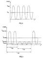
- Figs. 4 and 5 depict the contrast between a continuous RF bias power wave form, such as that typically employed in the prior art etch, and the pulsed RF bias power wave form employed to reduce mask erosion in accordance with the present invention.
- the prior art continuous RF power wave form has a predefined RF frequency, e.g., 4 MHz, a predefined maximum power level P MAX , thereby yielding an average power level P AV .
- the RF bias power wave form of prior art Fig. 4 is deemed continuous since the amplitude of the wave form does not vary from the predefined maximum power level P MAX during etching.
- the RF power is also supplied at a predefined RF frequency (although a constant RF frequency is not required by the invention).
- the maximum amplitude of the RF bias power wave form of Fig. 5 alternates between a high power level P MAX-HIGH and a low power level P MAX-LOW .
- the average power (P AV-LOW ) delivered to the chuck electrode is lower than the average power delivered to the chuck electrode during the high power cycle (P AV-HIGH ).
- the RF bias power wave form alternates between the low power level and the high power level at a predefined pulsed frequency f PULSE , which is the inverse of the pulse period (506) shown.
- the duty cycle is defined by the ratio of the duration of the high power cycle (502) relative to the duration of the pulse period (506).
- the pulse frequency i.e., the frequency at which the RF power supplied to the chuck electrode alternates between the high power level and the low power level
- the pulse frequency is selected to be sufficiently low to permit polymer to be deposited on the mask surface during the low power cycle.
- this deposited polymer acts as a sacrificial layer to afford some protection to the underlying mask material. Accordingly, even if the entire thickness of the deposited polymer is eroded away during the high power cycle, less of the mask material is etched away since the presence of the deposited polymer at the start of the high power cycle reduces the amount of time the mask material is exposed to the etchant material during this high power level.
- This aspect of the present invention flows from the recognition that in most plasma etching processes, two separate mechanisms are at work in competition against each other.
- RF power supplied to the chuck electrodes causes ions from the plasma to be accelerated toward the substrate surface to etch away areas of the underlying layer that are exposed through openings in the mask.
- polymer is deposited on the substrate, along the etch feature side wall, and along the bottom of the etched feature.
- the polymer deposition serves some useful functions, e.g., protecting the side wall from being attacked by the etchant during etching and preserving the etch profile.
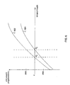
- Fig. 6 depicts an exemplary plot of etch rates versus RF bias power for a hypothetical etching process.
- the RF power wave form is assumed to be continuous (i.e., not pulsed) for ease of understanding.
- curve 602 depicts the etch rate through the underlying layer (e.g., a dielectric layer that underlies the mask).
- etching of the underlying layer occurs when RF bias power is above the predefined value P A .
- the etching mechanism and the polymer deposition mechanism cancel each other out, resulting in an etch rate of zero for the underlying layer.
- the polymer deposition mechanism becomes the dominant mechanism, and the polymer deposition is built up without etching of the underlying layer.
- Curve 604 depict the etch rate or the erosion rate through the mask as a function of RF bias power. Erosion of the mask occurs when RF bias power is above a predefined value P B . At the predefined value P B , the etching mechanism and the polymer deposition mechanism cancel each other out, resulting in an erosion rate of zero for the mask. Below the predefined value P B , the polymer deposition mechanism becomes the dominant mechanism and the polymer deposition is built up without erosion of the mask.
- etching of the underlying layer may still occur in the region between the values P A and P B while mask erosion is substantially minimized.
- the continuous RF power is reduced so that etching occurs only in this regime, the etch rate is typically too low to be of practical value.
- the etch rate at the bottom of the feature may actually slow down to the point where no etching of the underlying layer occurs as fewer and fewer ions reach the bottom of the etched feature.
- etching in accordance with prior art continuous RF power wave form technique typically employs a continuous RF bias power setting substantially higher than the value P B to increase the etch rate and/or to ensure that etching continues as the etch feature becomes deeper and deeper.
- mask erosion may be reduced by permitting the power level of the RF bias power to alternate between a low power level (e.g., below P B where polymer is permitted to deposit above the mask) and a high power level (e.g., above P A where etching of the underlying layer is increased but erosion of the deposited polymer/mask is also increased).
- a low power level e.g., below P B where polymer is permitted to deposit above the mask
- a high power level e.g., above P A where etching of the underlying layer is increased but erosion of the deposited polymer/mask is also increased.
- the polymer deposited on the mask surface during the low power cycle acts as a sacrificial layer to be eroded away first when the high power cycle resumes. In this manner, erosion of the mask material is reduced even if all of the deposited polymer is etched away at some point during the high power cycle.
- polymer deposition generally occurs faster on the surface of the mask than at the bottom of the etched feature or along the feature side walls. Since less polymer is deposited along the feature side walls and along the bottom of the etched feature during the low power cycle, the presence of the polymer deposition does not significantly reduce the etch rate at the bottom of the underlying layer or significantly degrade the etch profile (due to excessive side wall deposition). In some cases, it is possible to configure the etch recipe during the low power cycle (e.g., the power level, the duty cycle, the pulse frequency, or the like) such that little or no polymer is deposited at the bottom of the etched feature (or even to have some underlying layer etch) while polymer is deposited above the mask.
- the etch recipe e.g., the power level, the duty cycle, the pulse frequency, or the like
- the etch recipe is configured such that substantially all the polymer deposited along the etched feature side wall and at the bottom of the etched feature during the low power cycle be removed so that the etch profile may be preserved and etching through the underlying layer is expedited.
- the pulse period be sufficiently low to permit polymer deposition to occur during the low power cycle. If the pulse frequency is too high, e.g., above I kHz for most plasma processing systems, polymer deposition may not occur during the low power cycle. While not wishing to be bound by theory, it is believed that polymer deposition does not occur immediately upon the transition from the high power cycle to the low power cycle of the RF bias power wave form. This is because the substrate, the chuck, and the associated electronics have a nontrivial capacitance and a natural ramp down rate when the RF power level changes. Further, ions from the plasma typically have some nontrivial inertia and may take some time to lose their energy (i.e., to reduce the etching mechanism).
- Figs. 7-9 illustrate the effect on the etching and polymer deposition mechanisms at various RF bias power levels on an exemplary substrate stack.
- the RF bias power level is set at zero.
- a zero RF bias power level (or very low RF bias power level) causes polymer to be deposited above mask 702, along the side walls of etched feature (via) 704, and along the bottom of the etched feature.
- more polymer tends to be deposited above mask 702 than along the side walls of the etched feature or along the bottom of the etched feature.
- the polymer deposition along the bottom of the etched feature is removed to permit etching of the underlying layer 706 to proceed.
- the thickness of the deposited polymer along the upper surface of the mask retards erosion of the mask during the high power cycle.
- the RF bias power level is higher in Fig. 8 than the RF bias power level of Fig. 7 to depict the etch effect when the RF bias power is raised.
- polymer is deposited above mask 702. Due to the higher RF bias power level, however, little if any polymer deposition occurs along the feature side wall and along the bottom of the etched feature during the low power cycle. Further, some etching of the underlying layer may even occur during this low power cycle. As explained earlier in connection with Fig. 6, underlying etch may occur even though polymer continues to be deposited on the mask surface. When the high power cycle resumes, etching at the bottom of the feature continues while the thickness of the deposited polymer along the upper surface of the mask retards erosion of the mask.
- the RF bias power is even higher than that of Figs. 7 or 8 to depict the effect during the high power cycle.
- a relatively high RF bias power level there is significant etching through underlying layer 706. If a low power cycle precedes this high power cycle, most (or all) of the polymer deposited during the previous low power cycle is preferably removed. Although some mask material may be removed by the end of the high power cycle, the presence of the deposited polymer at the beginning of the high power cycle reduces the amount of mask material removed during this high power cycle.
- the pulse frequency may be varied. In general, decreasing the pulse frequency tends to increase the rate of polymer deposition (and therefore the mask selectivity).
- the duty cycle may be varied. In general, increasing the duty cycle tends to decrease mask selectivity. As the duty cycle of the RF bias power wave form approaches the 100% mark, the etch result approaches that of the prior art continuous RF bias wave form.
- the high power level may be varied to achieved the desired etch result during the high power cycle. For example, increasing the high power level tends to increase the etch rate and improve the vertical etch profile, albeit at a high mask erosion rate.
- the bottom power level may be varied to achieve the desired balance between the etch mechanism and the polymer deposition mechanism during the low power cycle. For example, increasing the low power level tends to increase the etch rate and reduce the amount of polymer deposition. With reference to Figs. 7 and 8, increasing the low power level tends to lower line 708. Conversely, reducing the low power level tends to reduce the etch rate, thereby permitting more polymer deposition to occur during the low power cycle.
- the low power level may be selected, in some cases, such that little or no polymer deposition occurs at the bottom of the etch feature (thereby minimizing any adverse effect on the etch rate through the underlying layer) while permitting some polymer deposition to occur at the top surface of the mask (to increase mask selectivity during etching).
- a 200 mm wafer having thereon a dielectric layer e.g., a silicon-dioxide containing layer (e.g., BPSG) is etched in the aforementioned TCPTM 9100 plasma processing system.
- the mask material represents a photoresist layer and the etchant includes a fluorocarbon-containing gas (e.g., a fluorocarbon gas or a hydrofluorocarbon gas such as C 2 HF 5 ).
- a fluorocarbon-containing gas e.g., a fluorocarbon gas or a hydrofluorocarbon gas such as C 2 HF 5 .
- the specific etchant chosen depends on the etch recipe chosen and/or the composition of the underlying layer to be etched.
- the high RF bias power level is about 1600 watts. However, the high RF bias power level may be optimized to achieve a suitable overall dielectric etch rate, photoresist selectivity, and to maintain the desired etch profile in a given system and/or for a given substrate stack.
- the high RF bias power level may be between about 600 and about 2500 watts.
- the low power level may be between about 0 watts to about 1 ⁇ 2 of the high power level, preferably between about 0 watts to about 1/5 of the high power level. In this example, the low power level is about 150 watts.
- the duty cycle may vary between about 10% and any value below 100%, more preferably between about 30% and about 75%. In this example, the duty cycle is about 50%.
- the pulse period may vary between 0.1 Hz to any value below 1000 Hz, more preferably between about 1 Hz to about 100 Hz and preferably at about 5 Hz.
- the pressure within the aforementioned TCPTM 9100 reactor is maintained at about 6.7 x 10 -2 kgm -2 (5 m Torr) during etching.
- the top power is set at about 1500 watts.
- the top RF power is continuous.
- the top RF power may also be pulsed if desired.
- Argon is flowed into the processing chamber at about 100 standard cubic centimeters per minute (sccm) (1.6 x 10 -6 m 3 s -1 ).
- any suitable substantially nonreactive gas including, for example, a noble gas or N 2 ) may also be employed.
- CHF 3 is also flowed at about 7.2 X 10 -5 m 3 s -1 (45 sccm)
- C 2 HF 5 is flowed at about 3.2 x 10 -6 m 3 s -1 (20 sccm)
- CH 2 F 2 is flowed at about 8 x 10 -7 m 3 s -1 (5 sccm). It should be understood, however, that the invention is not limited to pressure, top power setting and flow rates of the specific embodiment. From this disclosure, one skilled in the art would readily recognise that such parameters may be varied to suit the requirements of a particular plasma processing system and/or a particular substrate.
- photoresist selectivity increases from about 3:1 to about 7:1 without significant adverse impact on the etch profile and/or the etch rate. It is expected that improvements may be obtained even for etches that, when etched with continuous RF power wave forms, already have a higher mask selectivity.
- the result shows a significant improvement over prior art etches utilizing only continuous RF power wave forms wherein improving mask selectivity, i.e., reducing mask erosion, often results in degraded etch profile and/or reduced overall underlying layer etch rate (and the converse situation wherein improving the etch profile often comes at the expense of mask selectivity, i.e., at the expense of increased mask erosion).
Landscapes
- Physics & Mathematics (AREA)
- Engineering & Computer Science (AREA)
- Plasma & Fusion (AREA)
- Chemical & Material Sciences (AREA)
- Analytical Chemistry (AREA)
- Drying Of Semiconductors (AREA)
Claims (10)
- Procédé destiné à réduire l'érosion de masque lors de la gravure d'un trou d'interconnexion (704) au travers d'un enduit photorésistant (702) dans une couche diélectrique (706) sous-jacente à un masque (702), ladite couche diélectrique étant disposée sur un substrat (310), ledit substrat étant placé sur un mandrin (312) dans une chambre de traitement au plasma (302), comprenant les étapes consistant à :faire circuler un gaz de gravure source dans ladite chambre de traitement au plasma, ledit gaz de gravure source comprenant du gaz contenant du fluorocarbure et un gaz sensiblement non-réactif ;constituer un plasma à partir dudit gaz de gravure source ; etfournir une forme d'onde d'énergie d'impulsion radioélectrique audit mandrin, ladite forme d'onde d'énergie d'impulsion radioélectrique présentant une première fréquence et alternant entre un cycle de forte puissance et un cycle de faible puissance à une fréquence d'impulsion, en sélectionnant un niveau de puissance maximale (Pmax-low) pendant ledit cycle de faible puissance et ladite fréquence d'impulsion entraínant ainsi le dépôt de polymère sur ledit masque pendant ledit cycle de faible puissance, dans lequel le polymère déposé est une couche protectrice sacrificielle pour la gravure pendant ledit cycle de puissance élevée.
- Procédé selon la revendication 1, dans lequel le niveau de puissance maximale (Pmax-high) pendant ledit cycle de puissance élevée est sélectionné pour permettre la gravure dudit matériau diélectrique au fond dudit trou d'interconnexion (704) pendant le cycle de puissance élevée.
- Procédé selon la revendication 1, dans lequel un niveau de puissance maximale (Pmax-high) pendant le cycle de puissance élevée est sélectionné pour retirer, vers la fin dudit cycle de puissance élevée, sensiblement tout le polymère déposé sur le fond dudit trou d'interconnexion pendant ledit cycle de faible puissance.
- Procédé selon la revendication 3, dans lequel ledit niveau de puissance maximale (Pmax-high) pendant ledit cycle de puissance élevée est sélectionné pour retirer, vers ladite fin dudit cycle de forte puissance, sensiblement tout le polymère déposé le long des parois latérales dudit trou d'interconnexion pendant ledit cycle de faible puissance.
- Procédé selon l'une quelconque des revendications 4, dans lequel ladite fréquence d'impulsion se situe entre 0,1 Hz et 1kHz.
- Procédé selon la revendication 5, dans lequel ladite fréquence d'impulsion se situe entre 5 Hz et 100 Hz.
- Procédé selon la revendication 6, dans lequel le niveau de puissance maximale (Pmax-low) pendant ledit cycle de faible puissance est inférieur à la moitié du niveau de puissance maximale(Pmax-high) pendant ledit cycle de puissance élevée.
- Procédé selon l'une quelconque des revendications précédentes comprenant en outre l'alimentation en puissance radioélectrique d'une électrode supérieure (304) de ladite chambre de traitement au plasma (302), ladite électrode supérieure étant disposée au-dessus dudit substrat (310).
- Procédé selon la revendication 8, dans lequel ladite électrode supérieure (304) représente une bobine d'induction.
- Procédé selon l'une quelconque des revendications précédentes, dans lequel le niveau de puissance élevée est sélectionné pour retirer sensiblement tout le dépôt de polymère du fond du trou d'interconnexion (704) pendant le cycle de puissance élevée.
Applications Claiming Priority (3)
| Application Number | Priority Date | Filing Date | Title |
|---|---|---|---|
| US09/018,448 US6093332A (en) | 1998-02-04 | 1998-02-04 | Methods for reducing mask erosion during plasma etching |
| US18448 | 1998-02-04 | ||
| PCT/US1999/002224 WO1999040607A1 (fr) | 1998-02-04 | 1999-02-02 | Procedes de reduction de l'erosion du masque lors de la gravure au plasma |
Publications (2)
| Publication Number | Publication Date |
|---|---|
| EP1053563A1 EP1053563A1 (fr) | 2000-11-22 |
| EP1053563B1 true EP1053563B1 (fr) | 2003-07-02 |
Family
ID=21787981
Family Applications (1)
| Application Number | Title | Priority Date | Filing Date |
|---|---|---|---|
| EP99904542A Expired - Lifetime EP1053563B1 (fr) | 1998-02-04 | 1999-02-02 | Procedes de reduction de l'erosion du masque lors de la gravure au plasma |
Country Status (7)
| Country | Link |
|---|---|
| US (2) | US6093332A (fr) |
| EP (1) | EP1053563B1 (fr) |
| JP (1) | JP4548561B2 (fr) |
| KR (1) | KR100604741B1 (fr) |
| AT (1) | ATE244453T1 (fr) |
| DE (1) | DE69909248T2 (fr) |
| WO (1) | WO1999040607A1 (fr) |
Families Citing this family (38)
| Publication number | Priority date | Publication date | Assignee | Title |
|---|---|---|---|---|
| KR100521120B1 (ko) * | 1998-02-13 | 2005-10-12 | 가부시끼가이샤 히다치 세이사꾸쇼 | 반도체소자의 표면처리방법 및 장치 |
| KR100528685B1 (ko) * | 1998-03-12 | 2005-11-15 | 가부시끼가이샤 히다치 세이사꾸쇼 | 시료의 표면 가공방법 |
| US6492277B1 (en) * | 1999-09-10 | 2002-12-10 | Hitachi, Ltd. | Specimen surface processing method and apparatus |
| KR100829288B1 (ko) * | 1998-12-11 | 2008-05-13 | 서페이스 테크놀로지 시스템스 피엘씨 | 플라즈마 처리장치 |
| US6255221B1 (en) * | 1998-12-17 | 2001-07-03 | Lam Research Corporation | Methods for running a high density plasma etcher to achieve reduced transistor device damage |
| JP4351755B2 (ja) * | 1999-03-12 | 2009-10-28 | キヤノンアネルバ株式会社 | 薄膜作成方法および薄膜作成装置 |
| KR100750420B1 (ko) * | 1999-08-17 | 2007-08-21 | 동경 엘렉트론 주식회사 | 플라즈마 보조 처리 실행 방법 및 플라즈마 보조 처리실행 리액터 |
| JP2001168086A (ja) | 1999-12-09 | 2001-06-22 | Kawasaki Steel Corp | 半導体装置の製造方法および製造装置 |
| US20020185226A1 (en) * | 2000-08-10 | 2002-12-12 | Lea Leslie Michael | Plasma processing apparatus |
| DE10309711A1 (de) * | 2001-09-14 | 2004-09-16 | Robert Bosch Gmbh | Verfahren zum Einätzen von Strukturen in einem Ätzkörper mit einem Plasma |
| JP2005531125A (ja) * | 2001-10-22 | 2005-10-13 | ユナクシス・ユーエスエイ・インコーポレーテッド | パルス化プラズマを使用したフォトマスク基板のエッチングのための方法及び装置 |
| TW567394B (en) * | 2001-10-22 | 2003-12-21 | Unaxis Usa Inc | Apparatus for processing a photomask, method for processing a substrate, and method of employing a plasma reactor to etch a thin film upon a substrate |
| EP1444727A4 (fr) * | 2001-10-22 | 2007-07-18 | Unaxis Usa Inc | Procede et appareil de gravure de couches minces sensibles a la deterioration a l'aide d'un plasma a impulsions haute frequence |
| TWI315966B (en) * | 2002-02-20 | 2009-10-11 | Panasonic Elec Works Co Ltd | Plasma processing device and plasma processing method |
| US20030235998A1 (en) * | 2002-06-24 | 2003-12-25 | Ming-Chung Liang | Method for eliminating standing waves in a photoresist profile |
| US20040097077A1 (en) * | 2002-11-15 | 2004-05-20 | Applied Materials, Inc. | Method and apparatus for etching a deep trench |
| US6759339B1 (en) * | 2002-12-13 | 2004-07-06 | Silicon Magnetic Systems | Method for plasma etching a microelectronic topography using a pulse bias power |
| US7976673B2 (en) * | 2003-05-06 | 2011-07-12 | Lam Research Corporation | RF pulsing of a narrow gap capacitively coupled reactor |
| US7446050B2 (en) * | 2003-08-04 | 2008-11-04 | Taiwan Semiconductor Manufacturing Co., Ltd. | Etching and plasma treatment process to improve a gate profile |
| JP2005072260A (ja) * | 2003-08-25 | 2005-03-17 | Sanyo Electric Co Ltd | プラズマ処理方法、プラズマエッチング方法、固体撮像素子の製造方法 |
| US7879510B2 (en) * | 2005-01-08 | 2011-02-01 | Applied Materials, Inc. | Method for quartz photomask plasma etching |
| WO2008021609A1 (fr) * | 2006-08-07 | 2008-02-21 | Tokyo Electron Limited | Procédé de traitement d'une couche de masque préalable à la mise en oeuvre d'un processus de gravure |
| US7572386B2 (en) | 2006-08-07 | 2009-08-11 | Tokyo Electron Limited | Method of treating a mask layer prior to performing an etching process |
| US7642193B2 (en) * | 2006-08-07 | 2010-01-05 | Tokyo Electron Limited | Method of treating a mask layer prior to performing an etching process |
| US7449414B2 (en) * | 2006-08-07 | 2008-11-11 | Tokyo Electron Limited | Method of treating a mask layer prior to performing an etching process |
| US8192576B2 (en) * | 2006-09-20 | 2012-06-05 | Lam Research Corporation | Methods of and apparatus for measuring and controlling wafer potential in pulsed RF bias processing |
| JP5192209B2 (ja) | 2006-10-06 | 2013-05-08 | 東京エレクトロン株式会社 | プラズマエッチング装置、プラズマエッチング方法およびコンピュータ読取可能な記憶媒体 |
| JP5514413B2 (ja) * | 2007-08-17 | 2014-06-04 | 東京エレクトロン株式会社 | プラズマエッチング方法 |
| JP5295748B2 (ja) * | 2008-12-18 | 2013-09-18 | 東京エレクトロン株式会社 | 構成部品の洗浄方法及び記憶媒体 |
| US9105705B2 (en) * | 2011-03-14 | 2015-08-11 | Plasma-Therm Llc | Method and apparatus for plasma dicing a semi-conductor wafer |
| CN103871865B (zh) * | 2012-12-18 | 2016-08-17 | 中微半导体设备(上海)有限公司 | 一种清洁等离子体反应腔侧壁的方法 |
| US9583485B2 (en) | 2015-05-15 | 2017-02-28 | Taiwan Semiconductor Manufacturing Company, Ltd. | Fin field effect transistor (FinFET) device structure with uneven gate structure and method for forming the same |
| US9818841B2 (en) | 2015-05-15 | 2017-11-14 | Taiwan Semiconductor Manufacturing Co., Ltd. | Semiconductor structure with unleveled gate structure and method for forming the same |
| US11417501B2 (en) | 2015-09-29 | 2022-08-16 | Hitachi High-Tech Corporation | Plasma processing apparatus and plasma processing method |
| JP6670692B2 (ja) | 2015-09-29 | 2020-03-25 | 株式会社日立ハイテク | プラズマ処理装置およびプラズマ処理方法 |
| US10886136B2 (en) * | 2019-01-31 | 2021-01-05 | Tokyo Electron Limited | Method for processing substrates |
| US11915932B2 (en) | 2021-04-28 | 2024-02-27 | Applied Materials, Inc. | Plasma etching of mask materials |
| KR20230147594A (ko) * | 2022-04-13 | 2023-10-23 | 주식회사 히타치하이테크 | 플라스마 처리 방법 및 플라스마 처리 디바이스 |
Family Cites Families (10)
| Publication number | Priority date | Publication date | Assignee | Title |
|---|---|---|---|---|
| FI62692C (fi) * | 1981-05-20 | 1983-02-10 | Valmet Oy | Pappersmaskinspress med bred presszon |
| US4500563A (en) * | 1982-12-15 | 1985-02-19 | Pacific Western Systems, Inc. | Independently variably controlled pulsed R.F. plasma chemical vapor processing |
| KR890004881B1 (ko) * | 1983-10-19 | 1989-11-30 | 가부시기가이샤 히다찌세이사꾸쇼 | 플라즈마 처리 방법 및 그 장치 |
| DE3733135C1 (de) * | 1987-10-01 | 1988-09-22 | Leybold Ag | Vorrichtung zum Beschichten oder AEtzen mittels eines Plasmas |
| DE69017744T2 (de) * | 1989-04-27 | 1995-09-14 | Fuji Electric Co Ltd | Gerät und Verfahren zur Bearbeitung einer Halbleitervorrichtung unter Verwendung eines durch Mikrowellen erzeugten Plasmas. |
| US4889588A (en) * | 1989-05-01 | 1989-12-26 | Tegal Corporation | Plasma etch isotropy control |
| US5468341A (en) * | 1993-12-28 | 1995-11-21 | Nec Corporation | Plasma-etching method and apparatus therefor |
| US5683538A (en) * | 1994-12-23 | 1997-11-04 | International Business Machines Corporation | Control of etch selectivity |
| US5614060A (en) * | 1995-03-23 | 1997-03-25 | Applied Materials, Inc. | Process and apparatus for etching metal in integrated circuit structure with high selectivity to photoresist and good metal etch residue removal |
| US5983828A (en) * | 1995-10-13 | 1999-11-16 | Mattson Technology, Inc. | Apparatus and method for pulsed plasma processing of a semiconductor substrate |
-
1998
- 1998-02-04 US US09/018,448 patent/US6093332A/en not_active Expired - Lifetime
-
1999
- 1999-02-02 EP EP99904542A patent/EP1053563B1/fr not_active Expired - Lifetime
- 1999-02-02 KR KR1020007008510A patent/KR100604741B1/ko active IP Right Grant
- 1999-02-02 DE DE69909248T patent/DE69909248T2/de not_active Expired - Lifetime
- 1999-02-02 JP JP2000530927A patent/JP4548561B2/ja not_active Expired - Lifetime
- 1999-02-02 WO PCT/US1999/002224 patent/WO1999040607A1/fr active IP Right Grant
- 1999-02-02 AT AT99904542T patent/ATE244453T1/de active
-
2000
- 2000-07-05 US US09/610,303 patent/US6489245B1/en not_active Expired - Lifetime
Also Published As
| Publication number | Publication date |
|---|---|
| JP4548561B2 (ja) | 2010-09-22 |
| DE69909248T2 (de) | 2004-05-27 |
| JP2002503029A (ja) | 2002-01-29 |
| KR100604741B1 (ko) | 2006-07-26 |
| KR20010040638A (ko) | 2001-05-15 |
| WO1999040607A1 (fr) | 1999-08-12 |
| US6093332A (en) | 2000-07-25 |
| EP1053563A1 (fr) | 2000-11-22 |
| US6489245B1 (en) | 2002-12-03 |
| ATE244453T1 (de) | 2003-07-15 |
| DE69909248D1 (de) | 2003-08-07 |
Similar Documents
| Publication | Publication Date | Title |
|---|---|---|
| EP1053563B1 (fr) | Procedes de reduction de l'erosion du masque lors de la gravure au plasma | |
| EP1070342B1 (fr) | Techniques de formation de tranchees dans une couche de silicium d'un substrat dans un procede de traitement au plasma haute densite | |
| KR100590370B1 (ko) | 플라즈마 에칭 방법 | |
| JP4657458B2 (ja) | 低容量の誘電体層をエッチングするための技術 | |
| EP0702391B1 (fr) | Procédé de gravure et réacteur à plasma pour la mise en oeuvre dudit procédé | |
| US6489248B2 (en) | Method and apparatus for etch passivating and etching a substrate | |
| KR100718072B1 (ko) | 기판의 실리콘층에 직통으로 접촉홀을 형성하기 위한 방법 | |
| US6432832B1 (en) | Method of improving the profile angle between narrow and wide features | |
| EP1010203B1 (fr) | Procede d'attaque chimique d'une couche conductrice | |
| KR100595090B1 (ko) | 포토레지스트 마스크를 사용한 개선된 엣칭방법 | |
| US20030003748A1 (en) | Method of eliminating notching when anisotropically etching small linewidth openings in silicon on insulator | |
| JPH10150019A (ja) | フォトレジスト選択性を向上し重合体密着性を改善するためのプラズマ反応処理法 | |
| US6037267A (en) | Method of etching metallic film for semiconductor devices | |
| WO2023199371A1 (fr) | Procédé de traitement au plasma | |
| JP2917993B1 (ja) | ドライエッチング方法 | |
| EP4024438A1 (fr) | Procédé et appareil | |
| WO2001048789A1 (fr) | Procedes de traitement au plasma |
Legal Events
| Date | Code | Title | Description |
|---|---|---|---|
| PUAI | Public reference made under article 153(3) epc to a published international application that has entered the european phase |
Free format text: ORIGINAL CODE: 0009012 |
|
| 17P | Request for examination filed |
Effective date: 20000831 |
|
| AK | Designated contracting states |
Kind code of ref document: A1 Designated state(s): AT DE FR IE IT |
|
| 17Q | First examination report despatched |
Effective date: 20010518 |
|
| GRAH | Despatch of communication of intention to grant a patent |
Free format text: ORIGINAL CODE: EPIDOS IGRA |
|
| GRAH | Despatch of communication of intention to grant a patent |
Free format text: ORIGINAL CODE: EPIDOS IGRA |
|
| GRAA | (expected) grant |
Free format text: ORIGINAL CODE: 0009210 |
|
| AK | Designated contracting states |
Designated state(s): AT DE FR IE IT |
|
| REG | Reference to a national code |
Ref country code: IE Ref legal event code: FG4D |
|
| REF | Corresponds to: |
Ref document number: 69909248 Country of ref document: DE Date of ref document: 20030807 Kind code of ref document: P |
|
| PLBE | No opposition filed within time limit |
Free format text: ORIGINAL CODE: 0009261 |
|
| STAA | Information on the status of an ep patent application or granted ep patent |
Free format text: STATUS: NO OPPOSITION FILED WITHIN TIME LIMIT |
|
| ET | Fr: translation filed | ||
| 26N | No opposition filed |
Effective date: 20040405 |
|
| PGFP | Annual fee paid to national office [announced via postgrant information from national office to epo] |
Ref country code: IE Payment date: 20100224 Year of fee payment: 12 |
|
| PGFP | Annual fee paid to national office [announced via postgrant information from national office to epo] |
Ref country code: IT Payment date: 20100224 Year of fee payment: 12 Ref country code: FR Payment date: 20100303 Year of fee payment: 12 |
|
| PGFP | Annual fee paid to national office [announced via postgrant information from national office to epo] |
Ref country code: DE Payment date: 20100226 Year of fee payment: 12 |
|
| PGFP | Annual fee paid to national office [announced via postgrant information from national office to epo] |
Ref country code: AT Payment date: 20110119 Year of fee payment: 13 |
|
| REG | Reference to a national code |
Ref country code: FR Ref legal event code: ST Effective date: 20111102 |
|
| REG | Reference to a national code |
Ref country code: IE Ref legal event code: MM4A |
|
| PG25 | Lapsed in a contracting state [announced via postgrant information from national office to epo] |
Ref country code: IT Free format text: LAPSE BECAUSE OF NON-PAYMENT OF DUE FEES Effective date: 20110202 |
|
| REG | Reference to a national code |
Ref country code: DE Ref legal event code: R119 Ref document number: 69909248 Country of ref document: DE Effective date: 20110901 |
|
| PG25 | Lapsed in a contracting state [announced via postgrant information from national office to epo] |
Ref country code: IE Free format text: LAPSE BECAUSE OF NON-PAYMENT OF DUE FEES Effective date: 20110202 Ref country code: FR Free format text: LAPSE BECAUSE OF NON-PAYMENT OF DUE FEES Effective date: 20110228 |
|
| REG | Reference to a national code |
Ref country code: AT Ref legal event code: MM01 Ref document number: 244453 Country of ref document: AT Kind code of ref document: T Effective date: 20120202 |
|
| PG25 | Lapsed in a contracting state [announced via postgrant information from national office to epo] |
Ref country code: AT Free format text: LAPSE BECAUSE OF NON-PAYMENT OF DUE FEES Effective date: 20120202 |
|
| PG25 | Lapsed in a contracting state [announced via postgrant information from national office to epo] |
Ref country code: DE Free format text: LAPSE BECAUSE OF NON-PAYMENT OF DUE FEES Effective date: 20110901 |