EP1052568B1 - Trennbarer Addier mit drei Eingängen - Google Patents
Trennbarer Addier mit drei Eingängen Download PDFInfo
- Publication number
- EP1052568B1 EP1052568B1 EP00303257A EP00303257A EP1052568B1 EP 1052568 B1 EP1052568 B1 EP 1052568B1 EP 00303257 A EP00303257 A EP 00303257A EP 00303257 A EP00303257 A EP 00303257A EP 1052568 B1 EP1052568 B1 EP 1052568B1
- Authority
- EP
- European Patent Office
- Prior art keywords
- adder
- inputs
- carry
- input
- adder circuit
- Prior art date
- Legal status (The legal status is an assumption and is not a legal conclusion. Google has not performed a legal analysis and makes no representation as to the accuracy of the status listed.)
- Expired - Lifetime
Links
- 230000000295 complement effect Effects 0.000 description 6
- 238000010586 diagram Methods 0.000 description 6
- 238000007792 addition Methods 0.000 description 5
- 238000001914 filtration Methods 0.000 description 1
Images

Classifications
-
- G—PHYSICS
- G06—COMPUTING; CALCULATING OR COUNTING
- G06F—ELECTRIC DIGITAL DATA PROCESSING
- G06F7/00—Methods or arrangements for processing data by operating upon the order or content of the data handled
- G06F7/38—Methods or arrangements for performing computations using exclusively denominational number representation, e.g. using binary, ternary, decimal representation
- G06F7/48—Methods or arrangements for performing computations using exclusively denominational number representation, e.g. using binary, ternary, decimal representation using non-contact-making devices, e.g. tube, solid state device; using unspecified devices
- G06F7/50—Adding; Subtracting
- G06F7/505—Adding; Subtracting in bit-parallel fashion, i.e. having a different digit-handling circuit for each denomination
- G06F7/509—Adding; Subtracting in bit-parallel fashion, i.e. having a different digit-handling circuit for each denomination for multiple operands, e.g. digital integrators
-
- G—PHYSICS
- G06—COMPUTING; CALCULATING OR COUNTING
- G06F—ELECTRIC DIGITAL DATA PROCESSING
- G06F2207/00—Indexing scheme relating to methods or arrangements for processing data by operating upon the order or content of the data handled
- G06F2207/38—Indexing scheme relating to groups G06F7/38 - G06F7/575
- G06F2207/3804—Details
- G06F2207/3808—Details concerning the type of numbers or the way they are handled
- G06F2207/3812—Devices capable of handling different types of numbers
- G06F2207/382—Reconfigurable for different fixed word lengths
-
- G—PHYSICS
- G06—COMPUTING; CALCULATING OR COUNTING
- G06F—ELECTRIC DIGITAL DATA PROCESSING
- G06F2207/00—Indexing scheme relating to methods or arrangements for processing data by operating upon the order or content of the data handled
- G06F2207/38—Indexing scheme relating to groups G06F7/38 - G06F7/575
- G06F2207/3804—Details
- G06F2207/3808—Details concerning the type of numbers or the way they are handled
- G06F2207/3828—Multigauge devices, i.e. capable of handling packed numbers without unpacking them
Definitions
- This invention relates to adders and more particularly to adders in which a split-add operation can be utilized to increase computational throughput.
- Addition forms the basis of many processing operations including counting, subtraction, multiplication and filtering.
- adder circuits that add binary numbers provide an implementation with a trade-off between the speed of completing the addition operation and the amount of hardware, as measured by area required on an integrated circuit, to complete an addition operation. While three binary number representations are available, sign-magnitude, one's complement, and two's complement, computations are more efficient using the two's complement number representation.
- Adders can be used to accomplish subtraction by generating the two's complement of the subtrahend and adding the minuend. The two's complement of the subtrahend can be generated internal to the adder by providing the subtrahend in one's complement representation and adding one using the carry-in input to the adder.
- a split adder is an adder that is capable of operating in a non-split mode on operands having a relatively large number of bits, and in split mode is capable of operating as more than one adder on operands having relatively fewer bits.
- Split adders are employed to take advantage of existing hardware where a tradeoff between precision and the number of adders can be made. and to gain additional computational throughput without requiring additional hardware.
- Split-adders in which the most significant bit portion of two operands are added in a first portion of an adder, and the least significant bit portions of two operands are added in a second portion of an adder are known. Known split-adders, however, can not accommodate more than two operands as inputs.
- JP52-155027 a pair of multi-input adders are described in which the carry-out outputs from one of the pair of adders are input into the second of the pair of adders.
- an integrated circuit includes an adder having a first adder circuit for receiving a portion of the operands to be summed, along with corresponding carry-in inputs.
- the first adder circuit provides a sum output and carry-out outputs.
- a second adder circuit receives another portion of the operands to be summed, along with the corresponding carry-in inputs. Multiplexers between the first and second adder circuits determine whether the carry-in inputs to the second adder circuit are the same as the carry-in inputs to the first adder circuit or whether the carry-in inputs to the second adder circuit are independent.
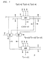
- Adder 10 may be fabricated as part of an integrated circuit, such as a microprocessor, microcontroller or digital signal processor. Adder 10 may be comprised of more than one multiple input adder, for example split adder 20 and split adder 30. The less significant bits of each of operands A, B and C are provided as inputs 22, 24 and 26 respectively to adder 20 operating as a three input adder. The more significant bits of each of operands A, B and C are provided as inputs 32, 34 and 36 respectively to adder 30 operating as a three-input adder.
- Each adder 20 and 30 receives as many carry-in inputs as it provides carry-out outputs. Typically the number of carry-in inputs and carry-out outputs is one less than the number of operands.
- the operands may be compressed from I to two inputs by an 1:2 compressor, not shown. See Computer Arithmetic Algorithms by I. Koren.
- Carry-in inputs 50 and 52 are provided to adder 20 and also as first inputs to respective multiplexers 60 and 58.
- Adder 20 operating as a three-input adder produces carry-out outputs 54 and 56 which provide, respectively, second inputs to multiplexers 60 and 58.
- a mode select signal 62 provides the carry select input to multiplexers 60 and 58.
- the carry select input takes on one of two states and determines which of the inputs to multiplexers 60 and 58 are selected as their respective outputs 70 and 68.
- Outputs 70 and 68 provide the carry-in inputs to three-input adder 30.
- Adder 20 operating as a three-input adder is a lower bit adder that receives inputs 22, 24 and 26 as well as carry-in inputs 50 and 52. Adder 20 provides a multiple bit sum 28 as an output that is the sum of the inputs. Adder 20 also provides carry-out outputs 54 and 56.
- Adder 30 is a higher bit adder that receives inputs 32, 34 and 36 as well as carry-in inputs 70 and 68. Adder 30 operating as a three-input adder provides a multiple bit sum 38 as an output that is the sum of the inputs. Adder 30 also provides carry-out outputs 72 and 74.
- Adders 20 and 30 may be any type of adder and may be operated as a single adder, or in a split-add mode as two independent adders, each with less precision than when operated as a single adder.
- the single adder mode of operation the lower order bits of each of the operands to be added are provided to adder 20 and the higher order bits of each of the operands to be added are provided to adder 30.
- each of adders 20 and 30 are capable of adding operands having the same number of bits, although the invention is not limited thereto.
- An example will be described in which three n-bit operands are added, with half of the bits (n/2 bits) of each operand provided to each adder, although the invention is not limited thereto.
- input 22 can represent the low order n/2 bits of input A, with input 32 representing the high order n/2 bits of input A.
- Input 24 can represent the low order n/2 bits of input B, with input 34 representing the high order n/2 bits of input B.
- input 26 can represent the low order n/2 bits of input C, with input 36 representing the high order n/2 bits of input C.
- carry-in inputs 50 and 52 are provided to adder 20.
- carry-in inputs 50 and 52 are typically zero.
- the carry-out outputs 54 and 56 from adder 20 become the carry-in inputs 70 and 68 to adder 30.
- Adder 20 operating as a three input adder receives inputs 22, 24 and 26 as well as carry-in inputs 50 and 52.
- Adder 20 provides as outputs a multiple bit sum output 28 representing n/2 of the lower order bits in the sum and carry-out outputs 54 and 56.
- the carry-out outputs from adder 20 are provided, based on the state of mode select signal 62, through multiplexers 60 and 58 as outputs 70 and 68 which are carry-in inputs to adder 30.
- Adder 30 provides a sum output representing n/2 high order bits in the sum and carry-out outputs 72 and 74.
- m operands each having n-bits, are added, the sum can have as many as [n+(m-1)] bits.
- Carry-out outputs 72 and 74 are used to calculate the highest order bit of the summation.
- adder 20 is capable of adding three operands, with adder 30 being capable of also adding three independent operands, albeit operands in the split-adder operation can have a total of as many bits as operands added by adder 10 operated as a single adder.
- the number of additions can be doubled by adders 20 and 30 operating independently of each other, where half of the precision of operating adders 20 and 30 as a single adder is required.
- operand inputs 22, 24 and 26 as well as carry-in inputs 50 and 52 are provided to adder 20.
- Adder 20 provides a multiple bit sum 28 that is the sum of operands 22, 24 and 26, as well as carry-in inputs 50 and 52.
- Adder 20 also provides carry-out outputs 54 and 64 which may be used elsewhere in the system. Carry-out outputs 54 and 56 are used to determine whether an overflow has occurred and possibly determine the highest order bit of the summation.
- Mode select signal 62 is generated to have one of two states to select inputs 64 and 66 as outputs from multiplexers 60 and 58. One skilled in the art would know how to generate a mode select signal having two states to accomplish the desired selection.
- inputs 64 and 66 provide the carry-in inputs 70 and 68 to adder 30.
- Operand inputs 32, 34 and 36 as well as carry-in inputs 70 and 68 are combined in adder 30 to provide multiple bit sum 38 that is the sum of the operand inputs and carry-in inputs.
- Adder 30 also provides carry-out outputs 72 and 74 which may be used elsewhere in the system. Carry-out outputs 72 and 74 are used to determine whether an overflow has occurred and possibly determine the highest order bit of the summation.
- adder 210 is shown in the schematic diagram of Figure 2.
- multiplexers 276 and 278 respectively are provided between carry-in input 250 and multiplexer 260 as well as between carry-input 252 and multiplexer 258.
- Multiplexers 276 and 278 permit carry-in inputs 282 and 284 to be provided to adder 230 operating as a three-input adder, independent of carry-in inputs 250 and 252, by select input 280 selecting as outputs from multiplexers 276 and 278 carry-in inputs 282 and 284.
- select input 280 selecting as outputs from multiplexers 276 and 278 carry-in inputs 282 and 284.
- One skilled in the art would know how to generate a mode select signal having two states to accomplish the desired carry-in input selection.
- multiplexers 260 and 258 through carry-select input 262 select outputs 264 and 266 from multiplexers 276 and 278 as carry-in inputs 270 and 268 to adder 230 operating as a three-input adder.
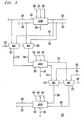
- adder 310 is shown in the schematic diagram of Figure 3 in which adder 310 can be split into three adders. The adders need not have the same number of bits in each operand.
- Adders 320, 330 and 340 are similar to adders 20 and 30 illustrated in Figure 1 and described above.
- Adder 320 receives three multiple bit inputs 322, 324 and 326 as well as carry-in inputs 350 and 352.
- Adder 320 combines the inputs to produce a sum output 328 and carry-out outputs 354 and 356.
- Carry-out outputs 354 and 356 are passed by multiplexers 360 and 358 to be carry-in inputs 368 and 370 when select input 362 is in a first state corresponding to the single adder mode, and when select input 362 is in a second state corresponding to the split adder mode, carry-in inputs 350 and 352 are selected as the carry-inputs 368 and 370.
- Adder 330 operating as a three-input adder receives three multiple bit inputs 332, 334 and 336 as well as carry-in inputs 368 and 370. Adder 330 combines the inputs to produce a sum output 338 and carry-out outputs 372 and 374. Carry-out outputs 372 and 374 from three-input adder 330 are passed by multiplexers 376 and 378 to be carry-in inputs 386 and 388 when select input 380 is in a first state corresponding to the single adder mode, and when select input 380 is in a second state corresponding to the split adder mode, carry-in inputs 382 and 384 are selected as the carry-in inputs 386 and 388, respectively.
- Adder 340 operating as a three-input adder receives three multiple bit inputs 342, 344 and 346 as well as carry-in inputs 386 and 388. Adder 340 combines the inputs to produce a sum output 348 and carry-out outputs 390 and 392. Carry-out outputs 372 and 374 are passed by multiplexers 376 and 378 to be carry-in inputs 386 and 388 when select input 380 is in a first state corresponding to the single adder mode, and when select input 380 is in a second state, carry-in inputs 382 and 384 are selected as the carry-in inputs 386 and 388 to three input adder 340, independent of the carry-in inputs to adders 320 and 330. Select inputs 362 and 380 may operate as if the same signal were applied to each or different signals are applied to each. One skilled in the art would know how to generate one or more mode select signals having two states to accomplish the desired selection.
- adder 310 includes adders 320, 330 and 340 operating as a single adder with carry-out outputs from adder 320 provided to adder 330 as carry-in inputs, and carry-out outputs from adder 330 are provided to adder 340 as carry-in inputs.
- the sum of the operands and carry-in inputs provided to adders 320, 330 and 340 is represented by the sum output 328 from adder 320 concatenated with the sum output 338 from adder 330 concatenated with the sum output 348 from adder 340.
- Carry-out outputs 390 and 392 from adder 340 are used to calculate the highest order bit in the summation.
Landscapes
- Physics & Mathematics (AREA)
- General Physics & Mathematics (AREA)
- Engineering & Computer Science (AREA)
- Computational Mathematics (AREA)
- Mathematical Analysis (AREA)
- Pure & Applied Mathematics (AREA)
- Theoretical Computer Science (AREA)
- Computing Systems (AREA)
- Mathematical Optimization (AREA)
- General Engineering & Computer Science (AREA)
- Complex Calculations (AREA)
Claims (8)
- Addierer (10) mit folgendem:einer ersten Addiererschaltung (20) zum Empfangen einer Mehrzahl k von Operanden (22, 24, 26) als Eingaben, wobei k eine Ganzzahl von mindestens drei ist, wobei die erste Addiererschaltung k-1 Übertragausgaben (54, 56) bereitstellt;einer zweiten Addiererschaltung (30) zum Empfangen einer Mehrzahl m von Operanden (32, 34, 36), wobei m eine Ganzzahl von mindestens drei ist, und m-1 Übertrageingaben (68, 70) als Eingaben, wobei die zweite Addiererschaltung als Ausgaben eine Summe bereitstellt, die eine Summe (38) der m Eingaben und der m-1 Übertrageingaben ist, wobei der Addierer (10) dadurch gekennzeichnet ist, daß die erste Addiererschaltung (20) zusätzlich k-1 Übertrageingaben (50, 52) als Eingaben empfängt, wodurch die erste Addiererschaltung eine Summe (28) als Ausgaben bereitstellt, die eine Summe der k Eingaben und der k-1 Übertrageingaben ist, und der Addierer weiterhin k-1 erste Multiplexer (58, 60) umfaßt, wobei jeder der k-1 ersten Multiplexer zum Empfangen einer entsprechenden der k-1 Übertrageingaben (50, 52) in die erste Addiererschaltung als erste Eingabe und einer entsprechenden der k-1 Übertragausgaben (54 oder 56) aus der ersten Addiererschaltung als zweite Eingabe geeignet ist, wobei jeder der k-1 ersten Multiplexer (58, 60) eine entsprechende erste Auswahleingabe (62) zum Auswählen eines der ersten Multiplexereingaben als entsprechende erste Multiplexerausgabe empfängt; so daß, wenn die erste Auswahleingabe einen ersten Zustand annimmt, die Übertragausgaben aus der ersten Addiererschaltung als Übertrageingaben in die zweite Addiererschaltung bereitgestellt werden und die erste Addiererschaltung und zweite Addiererschaltung als einzelne Addierer fungieren, und wenn die erste Auswahleingabe einen zweiten Zustand annimmt, die erste Addiererschaltung und die zweite Addiererschaltung getrennt als unabhängige Addierer fungieren.
- Addierer nach Anspruch 1, weiterhin dadurch gekennzeichnet, daß die Anzahl von Eingaben k in die erste Addiererschaltung (20) die gleiche wie die Anzahl von Eingaben m in die zweite Addiererschaltung (30) ist.
- Addierer nach Anspruch 1, weiterhin dadurch gekennzeichnet, daß die Operanden Mehrbitoperanden sind, die eine Summe erzeugen, die eine Mehrbitsumme ist.
- Addierer nach Anspruch 3, weiterhin dadurch gekennzeichnet, daß die Anzahl von Bit in den als Eingaben in die erste Addiererschaltung (20) bereitgestellten Operanden (22, 24, 26) die gleiche wie die Anzahl von Bit in den als Eingaben in die zweite Addiererschaltung (30) bereitgestellten Operanden (32, 34, 36) ist.
- Addierer (210) nach Anspruch 1, weiterhin gekennzeichnet durch k-1 zweite Multiplexer (276, 278), wobei jeder der zweiten Multiplexer zum Empfangen einer der k-1 Übertrageingaben (250 oder 252) als erste Eingabe und einer weiteren Übertrageingabe als zweite Eingabe (282 oder 284) geeignet ist, wobei jeder zweite Multiplexer (276, 278) auch zum Empfangen einer zweiten Auswahleingabe (280) zum Auswählen einer der Eingaben in den zweiten Multiplexer als entsprechende zusätzliche Multiplexerausgabe (264, 266) geeignet ist, wobei die k-1 Ausgaben (264, 266) des zweiten Multiplexers als entsprechende zweite Eingaben in die k-1 Multiplexer (260, 258) bereitgestellt werden.
- Addierer nach Anspruch 1, weiterhin dadurch gekennzeichnet, daß die zweite Addiererschaltung (30) weiterhin m-1 Übertragausgaben (372, 374) bereitstellt.
- Addierer nach Anspruch 6, weiterhin dadurch gekennzeichnet, daß er folgendes umfaßt: m-1 dritte Multiplexer (376, 378), wobei jeder der m-1 dritten Multiplexer zum Empfangen einer entsprechenden der m-1 Übertragausgaben aus der zweiten Addiererschaltung als erste Eingabe und einer entsprechenden zusätzlichen Übertrageingabe (382, 384) als zweite Eingabe geeignet ist, wobei jeder der m-1 dritten Multiplexer eine entsprechende dritte Auswahleingabe (380) zum Auswählen einer der Eingaben des dritten Multiplexers als entsprechende Ausgabe (386, 388) des dritten Multiplexers empfängt; und
eine dritte Addiererschaltung (340) zum Empfangen einer Mehrzahl n von Operanden (342, 344, 346) als Eingaben, wobei n eine Ganzzahl größer als zwei ist, und von n-1 Übertrageingaben (386, 388), wobei die dritte Addiererschaltung als Ausgabe (348) eine Summe bereitstellt, die eine Summe der n Mehrbiteingaben (342, 344, 346) und der n-1 Übertrageingaben (386, 388) ist. - Addierer nach einem beliebigen der Ansprüche 1 bis 7, weiterhin dadurch gekennzeichnet, daß der Addierer als integrierte Schaltung hergestellt wird.
Applications Claiming Priority (2)
| Application Number | Priority Date | Filing Date | Title |
|---|---|---|---|
| US09/310,404 US6449629B1 (en) | 1999-05-12 | 1999-05-12 | Three input split-adder |
| US310404 | 1999-05-12 |
Publications (2)
| Publication Number | Publication Date |
|---|---|
| EP1052568A1 EP1052568A1 (de) | 2000-11-15 |
| EP1052568B1 true EP1052568B1 (de) | 2004-01-28 |
Family
ID=23202348
Family Applications (1)
| Application Number | Title | Priority Date | Filing Date |
|---|---|---|---|
| EP00303257A Expired - Lifetime EP1052568B1 (de) | 1999-05-12 | 2000-04-18 | Trennbarer Addier mit drei Eingängen |
Country Status (4)
| Country | Link |
|---|---|
| US (1) | US6449629B1 (de) |
| EP (1) | EP1052568B1 (de) |
| JP (1) | JP3537378B2 (de) |
| KR (1) | KR100627993B1 (de) |
Families Citing this family (9)
| Publication number | Priority date | Publication date | Assignee | Title |
|---|---|---|---|---|
| US6584485B1 (en) * | 2000-04-14 | 2003-06-24 | International Business Machines Corporation | 4 to 2 adder |
| US6748411B1 (en) * | 2000-11-20 | 2004-06-08 | Agere Systems Inc. | Hierarchical carry-select multiple-input split adder |
| US7219118B2 (en) * | 2001-11-06 | 2007-05-15 | Broadcom Corporation | SIMD addition circuit |
| US7051062B2 (en) * | 2002-09-10 | 2006-05-23 | Analog Devices, Inc. | Apparatus and method for adding multiple-bit binary-strings |
| US7149768B2 (en) * | 2002-10-15 | 2006-12-12 | Ceva D.S.P. Ltd. | 3-input arithmetic logic unit |
| WO2010019169A1 (en) * | 2008-08-15 | 2010-02-18 | Lsi Corporation | Rom list-decoding of near codewords |
| KR102072543B1 (ko) * | 2013-01-28 | 2020-02-03 | 삼성전자 주식회사 | 복수 데이터 형식을 지원하는 가산기 및 그 가산기를 이용한 복수 데이터 형식의 가감 연산 지원 방법 |
| US10963220B2 (en) * | 2018-11-12 | 2021-03-30 | Samsung Electronics Co., Ltd. | Signed multiplication using unsigned multiplier with dynamic fine-grained operand isolation |
| CN111857651B (zh) * | 2020-06-16 | 2023-06-16 | 眸芯科技(上海)有限公司 | 用多比特加法器并行进行多个少比特加法的方法及应用 |
Citations (1)
| Publication number | Priority date | Publication date | Assignee | Title |
|---|---|---|---|---|
| JPS52155027A (en) * | 1976-06-18 | 1977-12-23 | Fujitsu Ltd | Multi-input adder for single-width data and double-width data |
Family Cites Families (13)
| Publication number | Priority date | Publication date | Assignee | Title |
|---|---|---|---|---|
| US4707800A (en) * | 1985-03-04 | 1987-11-17 | Raytheon Company | Adder/substractor for variable length numbers |
| JPS61239327A (ja) * | 1985-04-16 | 1986-10-24 | Nec Corp | オ−バフロ−検出方式 |
| JPS61255433A (ja) * | 1985-05-07 | 1986-11-13 | Mitsubishi Electric Corp | 演算装置 |
| JPH07113886B2 (ja) * | 1987-05-11 | 1995-12-06 | 株式会社日立製作所 | 演算回路 |
| US5189636A (en) * | 1987-11-16 | 1993-02-23 | Intel Corporation | Dual mode combining circuitry |
| JP2806171B2 (ja) * | 1992-08-31 | 1998-09-30 | 日本電気株式会社 | データ演算装置 |
| US5327369A (en) * | 1993-03-31 | 1994-07-05 | Intel Corporation | Digital adder and method for adding 64-bit, 16-bit and 8-bit words |
| EP0924601B1 (de) * | 1993-11-23 | 2001-09-26 | Hewlett-Packard Company, A Delaware Corporation | Parallele Datenverarbeitung in einem Einzelprozessor |
| US5390135A (en) * | 1993-11-29 | 1995-02-14 | Hewlett-Packard | Parallel shift and add circuit and method |
| US5883824A (en) * | 1993-11-29 | 1999-03-16 | Hewlett-Packard Company | Parallel adding and averaging circuit and method |
| US5493524A (en) * | 1993-11-30 | 1996-02-20 | Texas Instruments Incorporated | Three input arithmetic logic unit employing carry propagate logic |
| JP3356613B2 (ja) * | 1996-02-14 | 2002-12-16 | 日本電気株式会社 | 加算方法および加算器 |
| US6003125A (en) * | 1997-01-24 | 1999-12-14 | Texas Instruments Incorporated | High performance adder for multiple parallel add operations |
-
1999
- 1999-05-12 US US09/310,404 patent/US6449629B1/en not_active Expired - Lifetime
-
2000
- 2000-04-18 EP EP00303257A patent/EP1052568B1/de not_active Expired - Lifetime
- 2000-05-10 JP JP2000137224A patent/JP3537378B2/ja not_active Expired - Fee Related
- 2000-05-12 KR KR1020000025280A patent/KR100627993B1/ko not_active IP Right Cessation
Patent Citations (1)
| Publication number | Priority date | Publication date | Assignee | Title |
|---|---|---|---|---|
| JPS52155027A (en) * | 1976-06-18 | 1977-12-23 | Fujitsu Ltd | Multi-input adder for single-width data and double-width data |
Also Published As
| Publication number | Publication date |
|---|---|
| KR20010014902A (ko) | 2001-02-26 |
| JP3537378B2 (ja) | 2004-06-14 |
| US6449629B1 (en) | 2002-09-10 |
| JP2000330764A (ja) | 2000-11-30 |
| EP1052568A1 (de) | 2000-11-15 |
| KR100627993B1 (ko) | 2006-09-27 |
Similar Documents
| Publication | Publication Date | Title |
|---|---|---|
| US5790446A (en) | Floating point multiplier with reduced critical paths using delay matching techniques | |
| US3993891A (en) | High speed parallel digital adder employing conditional and look-ahead approaches | |
| US7395304B2 (en) | Method and apparatus for performing single-cycle addition or subtraction and comparison in redundant form arithmetic | |
| US9098332B1 (en) | Specialized processing block with fixed- and floating-point structures | |
| EP0992885B1 (de) | Multiplizier-Akkumulatorschaltungen | |
| US5508950A (en) | Circuit and method for detecting if a sum of two multibit numbers equals a third multibit constant number prior to availability of the sum | |
| US6366943B1 (en) | Adder circuit with the ability to detect zero when rounding | |
| JPH07210368A (ja) | 算術演算の結果として生じる正および負のオーバーフローのハードウェアによる効率的な取り扱い方法 | |
| WO1996028774A1 (en) | Exponentiation circuit utilizing shift means and method of using same | |
| US5508952A (en) | Carry-lookahead/carry-select binary adder | |
| US5892698A (en) | 2's complement floating-point multiply accumulate unit | |
| JPH01112332A (ja) | 乗算及び算術論理演算機能を組合わせて使用する浮動小数点ユニット | |
| EP1052568B1 (de) | Trennbarer Addier mit drei Eingängen | |
| US5862068A (en) | Arithmetic circuit for calculating a square-root of a sum of squares | |
| WO2018057111A1 (en) | Distributed double-precision floating-point multiplication | |
| US7139789B2 (en) | Adder increment circuit | |
| JP3306497B2 (ja) | 浮動小数点乗算器における丸め回路 | |
| US4956802A (en) | Method and apparatus for a parallel carry generation adder | |
| JPH04165530A (ja) | 浮動小数点乗算装置 | |
| Neto et al. | Decimal addition on FPGA based on a mixed BCD/excess-6 representation | |
| US7124162B2 (en) | Adder tree structure digital signal processor system and method | |
| JPH11296346A (ja) | 浮動小数点2進4倍長語フォ―マット乗算命令装置 | |
| US20080071852A1 (en) | Method to perform a subtraction of two operands in a binary arithmetic unit plus arithmetic unit to perform such a method | |
| US6748411B1 (en) | Hierarchical carry-select multiple-input split adder | |
| JPH04172526A (ja) | 浮動小数点除算器 |
Legal Events
| Date | Code | Title | Description |
|---|---|---|---|
| PUAI | Public reference made under article 153(3) epc to a published international application that has entered the european phase |
Free format text: ORIGINAL CODE: 0009012 |
|
| AK | Designated contracting states |
Kind code of ref document: A1 Designated state(s): GB |
|
| AX | Request for extension of the european patent |
Free format text: AL;LT;LV;MK;RO;SI |
|
| 17P | Request for examination filed |
Effective date: 20010514 |
|
| RAP1 | Party data changed (applicant data changed or rights of an application transferred) |
Owner name: AGERE SYSTEMS OPTOELECTRONICS GUARDIAN CORPORATION |
|
| AKX | Designation fees paid |
Free format text: GB |
|
| REG | Reference to a national code |
Ref country code: DE Ref legal event code: 8566 |
|
| 17Q | First examination report despatched |
Effective date: 20020919 |
|
| GRAH | Despatch of communication of intention to grant a patent |
Free format text: ORIGINAL CODE: EPIDOS IGRA |
|
| GRAS | Grant fee paid |
Free format text: ORIGINAL CODE: EPIDOSNIGR3 |
|
| GRAA | (expected) grant |
Free format text: ORIGINAL CODE: 0009210 |
|
| AK | Designated contracting states |
Kind code of ref document: B1 Designated state(s): GB |
|
| REG | Reference to a national code |
Ref country code: GB Ref legal event code: FG4D |
|
| PLBE | No opposition filed within time limit |
Free format text: ORIGINAL CODE: 0009261 |
|
| STAA | Information on the status of an ep patent application or granted ep patent |
Free format text: STATUS: NO OPPOSITION FILED WITHIN TIME LIMIT |
|
| 26N | No opposition filed |
Effective date: 20041029 |
|
| PGFP | Annual fee paid to national office [announced via postgrant information from national office to epo] |
Ref country code: GB Payment date: 20140416 Year of fee payment: 15 |
|
| GBPC | Gb: european patent ceased through non-payment of renewal fee |
Effective date: 20150418 |
|
| PG25 | Lapsed in a contracting state [announced via postgrant information from national office to epo] |
Ref country code: GB Free format text: LAPSE BECAUSE OF NON-PAYMENT OF DUE FEES Effective date: 20150418 |