EP0924601B1 - Parallele Datenverarbeitung in einem Einzelprozessor - Google Patents
Parallele Datenverarbeitung in einem Einzelprozessor Download PDFInfo
- Publication number
- EP0924601B1 EP0924601B1 EP99107195A EP99107195A EP0924601B1 EP 0924601 B1 EP0924601 B1 EP 0924601B1 EP 99107195 A EP99107195 A EP 99107195A EP 99107195 A EP99107195 A EP 99107195A EP 0924601 B1 EP0924601 B1 EP 0924601B1
- Authority
- EP
- European Patent Office
- Prior art keywords
- partition
- bit
- operands
- bits
- circuitry
- Prior art date
- Legal status (The legal status is an assumption and is not a legal conclusion. Google has not performed a legal analysis and makes no representation as to the accuracy of the status listed.)
- Expired - Lifetime
Links
Images


Classifications
-
- G—PHYSICS
- G06—COMPUTING OR CALCULATING; COUNTING
- G06F—ELECTRIC DIGITAL DATA PROCESSING
- G06F7/00—Methods or arrangements for processing data by operating upon the order or content of the data handled
- G06F7/38—Methods or arrangements for performing computations using exclusively denominational number representation, e.g. using binary, ternary, decimal representation
- G06F7/48—Methods or arrangements for performing computations using exclusively denominational number representation, e.g. using binary, ternary, decimal representation using non-contact-making devices, e.g. tube, solid state device; using unspecified devices
- G06F7/52—Multiplying; Dividing
- G06F7/523—Multiplying only
- G06F7/53—Multiplying only in parallel-parallel fashion, i.e. both operands being entered in parallel
- G06F7/5324—Multiplying only in parallel-parallel fashion, i.e. both operands being entered in parallel partitioned, i.e. using repetitively a smaller parallel parallel multiplier or using an array of such smaller multipliers
-
- G—PHYSICS
- G06—COMPUTING OR CALCULATING; COUNTING
- G06F—ELECTRIC DIGITAL DATA PROCESSING
- G06F7/00—Methods or arrangements for processing data by operating upon the order or content of the data handled
- G06F7/38—Methods or arrangements for performing computations using exclusively denominational number representation, e.g. using binary, ternary, decimal representation
- G06F7/48—Methods or arrangements for performing computations using exclusively denominational number representation, e.g. using binary, ternary, decimal representation using non-contact-making devices, e.g. tube, solid state device; using unspecified devices
- G06F7/483—Computations with numbers represented by a non-linear combination of denominational numbers, e.g. rational numbers, logarithmic number system or floating-point numbers
-
- G—PHYSICS
- G06—COMPUTING OR CALCULATING; COUNTING
- G06F—ELECTRIC DIGITAL DATA PROCESSING
- G06F7/00—Methods or arrangements for processing data by operating upon the order or content of the data handled
- G06F7/38—Methods or arrangements for performing computations using exclusively denominational number representation, e.g. using binary, ternary, decimal representation
- G06F7/48—Methods or arrangements for performing computations using exclusively denominational number representation, e.g. using binary, ternary, decimal representation using non-contact-making devices, e.g. tube, solid state device; using unspecified devices
- G06F7/50—Adding; Subtracting
- G06F7/505—Adding; Subtracting in bit-parallel fashion, i.e. having a different digit-handling circuit for each denomination
- G06F7/506—Adding; Subtracting in bit-parallel fashion, i.e. having a different digit-handling circuit for each denomination with simultaneous carry generation for, or propagation over, two or more stages
- G06F7/508—Adding; Subtracting in bit-parallel fashion, i.e. having a different digit-handling circuit for each denomination with simultaneous carry generation for, or propagation over, two or more stages using carry look-ahead circuits
-
- G—PHYSICS
- G06—COMPUTING OR CALCULATING; COUNTING
- G06F—ELECTRIC DIGITAL DATA PROCESSING
- G06F9/00—Arrangements for program control, e.g. control units
- G06F9/06—Arrangements for program control, e.g. control units using stored programs, i.e. using an internal store of processing equipment to receive or retain programs
- G06F9/30—Arrangements for executing machine instructions, e.g. instruction decode
- G06F9/30003—Arrangements for executing specific machine instructions
- G06F9/30007—Arrangements for executing specific machine instructions to perform operations on data operands
- G06F9/3001—Arithmetic instructions
- G06F9/30014—Arithmetic instructions with variable precision
-
- G—PHYSICS
- G06—COMPUTING OR CALCULATING; COUNTING
- G06F—ELECTRIC DIGITAL DATA PROCESSING
- G06F9/00—Arrangements for program control, e.g. control units
- G06F9/06—Arrangements for program control, e.g. control units using stored programs, i.e. using an internal store of processing equipment to receive or retain programs
- G06F9/30—Arrangements for executing machine instructions, e.g. instruction decode
- G06F9/30003—Arrangements for executing specific machine instructions
- G06F9/30007—Arrangements for executing specific machine instructions to perform operations on data operands
- G06F9/30036—Instructions to perform operations on packed data, e.g. vector, tile or matrix operations
- G06F9/30038—Instructions to perform operations on packed data, e.g. vector, tile or matrix operations using a mask
-
- G—PHYSICS
- G06—COMPUTING OR CALCULATING; COUNTING
- G06F—ELECTRIC DIGITAL DATA PROCESSING
- G06F2207/00—Indexing scheme relating to methods or arrangements for processing data by operating upon the order or content of the data handled
- G06F2207/38—Indexing scheme relating to groups G06F7/38 - G06F7/575
- G06F2207/3804—Details
- G06F2207/3808—Details concerning the type of numbers or the way they are handled
- G06F2207/3828—Multigauge devices, i.e. capable of handling packed numbers without unpacking them
Definitions
- the present invention concerns parallel data processing in a single processor system.
- each integer operand is 32 bits.
- each integer operand is 64 bits.
- an integer "add" instruction in a 64-bit computer, adds two 64-bit integer operands to produce a 64-bit integer result.
- a 64-bit add instruction takes one cycle of execution time.
- the pertinent range of operands is 16 bits or less. In current 32-bit and 64-bit computers, however, it still takes a full instruction to perform an operation on a pair of 16-bit operands. Thus the number of execution cycles required to perform an operation on two 16-bit operands is the same as the number of execution cycles required to perform the operation on two 32-bit operands in a 32-bit computer or two 64-bit operands in a 64-bit computer.
- a system which allows parallel data processing within a single processor.
- an arithmetic logic unit or other operation executing entity within the processing system such as a shifter is partitioned. Within each partition operations are performed. When the operation is to be performed on full word length operands, there is no parallel processing. Thus data is allowed to freely propagate across boundaries between the partitions.
- data is prevented from being propagated across at least one boundary between the partitions.
- each of the plurality of partitions performs an addition operation.
- the addition is to be performed on full word length operands, carries are allowed to propagate between the partitions.
- a carry is prevented from propagating across at least one boundary between the partitions.
- each of the plurality of partitions performs a shift operation.
- shifts are allowed between the partitions.
- a shift is prevented from crossing at least one boundary between the partitions.
- a multiplier implements both multiplication of whole word multiplicands and parallel multiplication of sub-word multiplicands.
- Circuitry for example an array of logic AND gates (or their equivalent), generates partial products.
- Partial product sum circuitry sums the partial products to produce a result.
- Partial product gating means in response to the selection of parallel multiplication of sub-word multiplicands, forces selected partial products to have a value of 0, thereby implementing parallel multiplication of sub-word multiplicands.
- the partial product gating means may be implemented, for example, using third inputs to at least a portion of the logic AND gates.
- the present invention allows for a single processor system to significantly increase performance by facilitating parallel processing operations when operands are less than the full word length. This inexpensive use of parallelism results in a huge increase in performance for computations that can utilize this type of data parallelism without significant additional cost in silicon space on a processor chip or complexity in design.
- the present invention also allows for parallel processing operations performed by a processor in response to a single instruction.
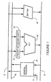
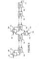
- Figure 1 shows a simplified block diagram of an operation execution data path within a processor in accordance with preferred embodiments of the present invention.
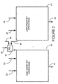
- FIG 2 shows a simplified block diagram of an arithmetic logic unit (ALU) shown in Figure 1 in accordance with a preferred embodiment of the present invention.
- ALU arithmetic logic unit
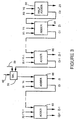
- Figure 3 shows an implementation of a two's complement adder within the ALU shown in Figure 2 in accordance with a preferred embodiment of the present invention.
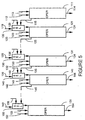
- Figure 4 shows an alternate simplified block diagram of the arithmetic logic unit (ALU) shown in Figure 1 in accordance with an . alternate preferred embodiment of the present invention.
- ALU arithmetic logic unit
- FIG 5 shows another alternate simplified block diagram of the arithmetic logic unit (ALU) shown in Figure 1 in accordance with another alternate preferred embodiment of the present invention.
- ALU arithmetic logic unit
- Figure 6 shows an implementation of a shifter shown in Figure 1 in accordance with a preferred embodiment of the present invention.
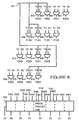
- Figure 7 shows a multiplier in accordance with the prior art.
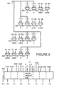
- Figure 8 and Figure 9 show a multiplier implemented in accordance with preferred embodiments of the present invention.
- Figure 10 shows an implementation of a carry look-ahead adder within the ALU shown in Figure 1 in accordance with an alternate preferred embodiment of the present invention.
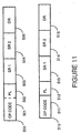
- Figure 11 shows an example of an instruction layout in accordance with an alternate preferred embodiment of the present invention.
- Figure 1 shows a simplified block diagram of an operation execution data path within a processor in accordance with preferred embodiments of the present invention.
- Operands for upcoming operations and results from accomplished operations are stored within general registers 25.
- a first operand stored in a first register within general registers 25 is placed on a first source bus 21. If the operation requires another operand, a second operand stored in a second register within general registers 25 is placed on a second source bus 22.
- ALU arithmetic logic unit
- a pre-shifter 27 and complement circuitry 28 may each be used to modify operands before they are received by ALU 26.
- the ALU may be partitioned to allow parallel data processing.
- Figure 2 shows ALU 26 divided into two partitions.
- a first partition 41 performs operations on low order bits 42 of a first operand and low order bits 43 of a second operand to produce low order bit results 44.
- a second partition 51 performs operations on high order bits 52 of the first operand and high order bits 53 of the second operand to produce high order bit results 54.
- a selector 50 is used to allow information on data path 45 to propagate from first partition 41 to second partition 51 or to intercept information on data path 45 before it is propagated from first partition 41 to second partition 51. Particularly, for arithmetic operations performed on full-word operands, information is allowed to propagate from first partition 41 through selector 50 to second partition 51. For the performance of parallel arithmetic operations on half-word operands, selector 50 prevents information from propagating from first partition 41 to second partition 51. Generally, in logic operations, there is no propagation of information from first partition 41 to second partition 51.
- each full-word operand is 32 bits. Therefore, when performing operations using 32-bit full word operands, selector 50 allows information to propagate from first partition 41 through selector 50 to second partition 51. When performing two parallel operations using 16-bit half word operands, selector 50 prevents information from propagating from first partition 41 through selector 50 to second partition 51. Instead the value on a line 59 is forwarded to partition 51.
- selector 50 When an "add" is being performed, a logic 0 is placed on input line 59.
- a logic 1 is placed on input line 59.
- a common arithmetic operation performed by ALU 26, shown in Figure 1 is two's complement addition.
- the use of two's complement circuitry 28 to perform a two's complement on an operand before performing a two's complement addition operation in the ALU implements a two's complement subtraction.
- the use of pre-shifter 27 to pre-shift an operand before performing a two's complement addition operation in the ALU implements a shift and add operation.
- FIG. 3 shows implementation of a two's complement adder with carry propagate addition within ALU 26 in accordance with a preferred embodiment of the present invention.
- ALU 26 includes a two's complement adder with carry look-ahead.
- a half adder 60 receives a single bit X 0 of a first operand and a single bit Y 0 of a second operand.
- Half adder 60 produces a sum bit Z 0 and a carry bit C 0 .
- a full adder 61 receives a single bit X 1 of the first operand, a single bit Y 1 of the second operand and carry bit C 0 .
- Full adder 61 produces a sum bit Z 1 and a carry bit C 1 .
- a full adder 65 receives a single bit X i-1 of the first operand, a single bit Y i-1 of the second operand and a carry bit from a previous adder (i.e., C i-2, not shown).
- Full adder 65 produces a sum bit Z i-1 and a carry bit C i-1.
- a full adder 66 receives a single bit X i of the first operand and a single bit Y i of the second operand.
- full adder 66 also receives, through selector 50 (or equivalent logic circuitry as will be understood by persons of ordinary skill in the art), carry bit C i-1.
- Full adder 66 produces a sum bit Z i and a carry bit C i .
- a full adder 69 receives a single bit X j-1 of the first operand, a single bit Y j-1 of the second operand and a carry bit from a previous adder (not shown).
- Full adder 69 produces a sum bit Z j-1 and a carry bit C j-1.
- Selector 50 is also shown in Figure 3.
- enable bit 49 is equal to logic one and allows a carry to propagate through selector 50 to full adder 66.
- enable bit 49 is equal to logic zero and prevents the carry from propagating through selector 50 to full adder 66. Instead the value on line 59 is forwarded to full adder 66.
- a logic 0 is placed on input line 59.
- a logic 1 is placed on input line 59.
- Figure 4 shows an alternate simplified block diagram of ALU 26 in accordance with an alternate preferred embodiment of the present invention.
- ALU 26 is divided into four partitions.
- a first partition 71 performs operations on low order bits 72 of a first operand and low order bits 73 of a second operand to produce low order bit results 74.
- a second partition 81 performs operations on bits 82 of the first operand and bits 83 of the second operand to produce result bits 84.
- a third partition 91 performs operations on bits 92 of the first operand and bits 93 of the second operand to produce result bits 94.
- a fourth partition 101 performs operations on high order bits 102 of the first operand and high order bits 103 of the second operand to produce high order bit results 104.
- a selector 80 is used to allow information on data path 75 to propagate from first partition 71 to second partition 81 or to intercept information on data path 75 before it is propagated from first partition 71 to second partition 81. Particularly, for arithmetic operations performed on full-word operands or half-word operands, information is allowed to propagate from first partition 71 through selector 80 to second partition 81. For the performance of parallel arithmetic operations on quarter-word operands, selector 80 prevents information from propagating from first partition 71 to second partition 81. Instead the value on a line 88 is forwarded to partition 81. When an "add" is being performed, a logic 0 is placed on line 88. When a "subtract" is being performed, a logic 1 is placed on line 88. Generally, in logic operations, there is no propagation of information between partitions.
- a selector 90 is used to allow information on data path 85 to propagate from second partition 81 to third partition 91 or to intercept information on data path 85 before it is propagated from second partition 81 to third partition 91. Particularly, for arithmetic operations performed on full-word operands, information is allowed to propagate from second partition 81 through selector 90 to third partition 91. For the performance of parallel arithmetic operations on quarter-word operands or half-word operands, selector 90 prevents information from propagating from second partition 81 to third partition 91. Instead the value on a line 98 is forwarded to partition 91. When an "add" is being performed, a logic 0 is placed on line 98. When a "subtract” is being performed, a logic 1 is placed on line 98.
- a selector 100 is used to allow information on data path 95 to propagate from third partition 91 to fourth partition 101 or to intercept information on data path 95 before it is propagated from third partition 91 to fourth partition 101. Particularly, for arithmetic operations performed on full-word operands and half-word operands, information is allowed to propagate from third partition 91 through selector 100 to fourth partition 101. For the performance of parallel arithmetic operations on quarter-word operands, selector 100 prevents information from propagating from third partition 91 to fourth partition 101. Instead the value on a line 108 is forwarded to partition 101. When an "add" is being performed, a logic 0 is placed on line 108. When a "subtract" is being performed, a logic 1 is placed on line 108.
- each full-word operand is 64 bits. Therefore, when performing operations using 64-bit full word operands, selector 80 allows information to propagate from first partition 71 through selector 80 to second partition 81, selector 90 allows information to propagate from second partition 81 through selector 90 to third partition 91, and selector 100 allows information to propagate from third partition 91 through selector 100 to fourth partition 101.
- selector 80 When performing two parallel operations using 32-bit half word operands, selector 80 allows information to propagate from first partition 71 through selector 80 to second partition 81, selector 90 prevents information from propagating from second partition 81 through selector 90 to third partition 91, and selector 100 allows information to propagate from third partition 91 through selector 100 to fourth partition 101.
- selector 80 When performing four parallel operations using 16-bit quarter word operands, selector 80 prevents information from propagating from first partition 71 through selector 80 to second partition 81, selector 90 prevents information from propagating from second partition 81 through selector 90 to third partition 91, and selector 100 prevents information from propagating from third partition 91 through selector 100 to fourth partition 101.
- FIG. 5 shows an another alternate simplified block diagram of ALU 26 in accordance with another alternate preferred embodiment of the present invention.
- ALU 26 is divided into partitions which are each one bit wide.
- a first partition 111 performs operations on a low order bit 112 of a first operand and on a low order bit 113 of a second operand to produce a low order result bit 114.
- a second partition 121 performs operations on a bit 122 of the first operand and a bit 123 of the second operand to produce a result bit 124.
- a partition 131 performs operations on a bit 132 of the first operand and a bit 133 of the second operand to produce a result bit 134.
- a partition 141 performs operations on a bit 142 of the first operand and a bit 143 of the second operand to produce a result bit 144.
- a partition 151 performs operations on a high order bit 152 of the first operand and a high order bit 153 of the second operand to produce a high order result bit 154.
- a selector 120 is used to allow information on data path 115 to propagate from first partition 111 to second partition 121 or to intercept information on data path 115 before it is propagated from first partition 111 to second partition 121.
- data is intercepted the value on a line 128 is forwarded to partition 121.
- a logic 0 is placed on line 128.
- a logic 1 is placed on line 128.
- a selector 130 is used to allow information on a data path from an immediately prior partition (not shown) to propagate from the immediately prior partition to partition 131 or to intercept information on the data path from the immediately prior partition before it is propagated to partition 131.
- data is intercepted the value on a line 138 is forwarded to partition 131.
- a logic 0 is placed on line 138.
- a logic 1 is placed on line 138.
- a selector 140 is used to allow information on data path 135 to propagate from partition 131 to partition 141 or to intercept information on data path 135 before it is propagated from partition 131 to partition 141.
- data is intercepted the value on a line 148 is forwarded to partition 141.
- a logic 0 is placed on line 148.
- a logic 1 is placed on line 148.
- a selector 150 is used to allow information on a data path from an immediately prior partition (not shown) to propagate from the immediately prior partition to partition 151 or to intercept information on the data path from the immediately prior partition before it is propagated to partition 151.
- data is intercepted the value on a line 158 is forwarded to partition 151.
- a logic 0 is placed on line 158.
- a logic 1 is placed on line 158.
- control inputs to the selectors may be used to allow parallel processing of operands of varying length.
- the control inputs could be selected so that parallel processing of two sixteen bit and four eight-bit arithmetic operations are all performed simultaneously.
- any bit combination which add up to no more than the word size could be used.
- parallel processing of seventeen bit, three bit, sixteen bit, twelve bit, five bit, and eleven bit arithmetic operations can also be performed simultaneously.
- a full adder 465 receives a single bit X i-1 of the first operand, a single bit Y i-1 of the second operand and a carry bit C i-2 .
- Full adder 465 produces a sum bit Z i-1 .
- a full adder 466 receives a single bit Xi of the first operand, a single bit Yi of the second operand and a carry bit C i-1 .
- Full adder 466 produces a sum bit Z i .
- a full adder 469 receives a single bit X j-1 of the first operand, a single bit Y j-1 of the second operand and a carry bit C j-2 .
- Full adder 469 produces a sum bit Z j-1 .
- "j" is the size of the data path and the bit length of full word operations. Also, “i” is equal to “j” divided by 2. For example, “j” is equal to 32 and “i” is equal to 16. Alternately, when j is equal to 32, i may be equal to any integer less than 32.
- an enable bit 452 When performing operations using "j"-bit full word operands, an enable bit 452 is equal to logic one and allows all carries to propagate. When performing two parallel operations using "i"-bit sub-word operands partitioned between bits i and i+1, enable bit 452 is equal to logic zero and prevents the carry propagating across the partition boundary. Instead the value on line 451 is used as the value forwarded to full adder 466. When an "add” is being performed, a logic 0 is placed on input line 451. When a "subtract” is being performed, a logic 1 is placed on input line 451.
- C[i-1] is the carry out of the previous bits of the carry look-ahead adder.
- the carry look-ahead adder works on generating these carry bits quickly.
- C[i-1] G[i-1] + P[i-1] * (G[I-2] + P[i-2] * (G[i-3] + P[i-3] * C[i-4]))
- C[i-2] G[i-2] + P[i-2] * (G[i-3] + P[i-3] * C[i-4J)
- C[i-3] G[i-3] + P[i-3] * C[i-4]
- Ps[i] Pm[i] Now if M[i] is 1, the value of Gs[i] is determined by F. If M [i] is 0 the value of Gs[i] is determined by A[i] and B[i] as it was previously. The propagate does not have to be forced by the F signal.
- FIG. 6 shows the present invention embodied in pre-shifter 27.
- the same embodiment of the present invention may also be used to implement shifter 29. Partitioning of pre-shifter 27 and shifter 29 allows, for example, for the implementation of parallel shift-and-add operations and parallel shift operations
- Pre-shifter 27 is shown to include a shift register one-bit slice 160, a shift register one-bit slice 161, a shift register one-bit slice 165, a shift register one-bit slice 166 and a shift register one-bit slice 169.
- a datum on input 171 When data is shifted to the left, a datum on input 171, typically a logic 0 value, is used as input to shift register one-bit slice 160.
- a selector 175 in response to a control input 182 selects either a datum on input 181 (a logic 0 value or a logic 1 value) or selects the value currently stored by shift register one-bit slice 169 to be input to shift register one-bit slice 169.
- Figure 6 shows the shifter partitioned between shift register one-bit slice 165 and shift register one-bit slice 166.
- selector 174 and a selector 173 have been added.
- selector 173 For shift operations on partitioned operands, when data is shifted to the left, selector 173, in response to a control input 185, selects a datum on input 172, typically a logic 0 value, to be used as input to shift register one-bit slice 166.
- selector 173 selects output from shift register one-bit slice 165 to be used as input to shift register one-bit slice 166.
- selector 174 For shift operations on partitioned operands, when data is shifted to the right, selector 174 in response to a control input 184 selects either a datum on input 183 (a logic 0 value or a logic 1 value) or selects the value currently stored by shift register one-bit slice 166 to be input to shift register one-bit slice 165. For shift operations on full word operands, when data is shifted to the right, selector 174 selects output from shift register one-bit slice 166 to be used as input to shift register one-bit slice 165.
- Figure 6 shows a shifter with only two partitions.
- the shifter can be partitioned in a variety of ways. For example, a 64-bit shifter may be partitioned into two, four, eight, sixteen, thirty-two or sixty-four bit equal size partitions. Additionally, it is not a requirement of the present invention that partitions each operate on equal number of bits.
- pre-shifter 27 and shifter 29 implemented as a shift register consisting of a series of one bit slices
- pre-shifter 27 is implemented by a one level of multiplexors, since it can usually shift by at most a small number of bits, for example, 0, 1, 2, 3 or 4 bits.
- Shifter 29 is typically implemented by three levels of multiplexors, where each level of multiplexor is a four-to-one multiplexor. For example, in a 64-bit shifter 29, the first level of multiplexors will shift either 0, 16, 32 or 48 bits. The second level of multiplexors can shift either 0, 4, 8 or 12 bits.
- the third level of multiplexors can shift 0, 1, 2 or 3 bits. This gives a shift of any number of bits from 0 to 63. In such a shifter built up of 3 stages of multiplexors, one-bit slices can still be identified. However the blocking of the shifts between any two bits may need to be done in one or more of the three multiplexer stages, as will be understood by those of ordinary skill in the art.
- a multiplier may be implemented in accordance with a preferred embodiment of the present invention to allow for partial word parallel multiplications in addition to whole word multiplications.
- Figure 7 shows a four-bit multiplier in accordance with the prior art.
- the multiplier multiplies a four-bit first multiplicand X 3 X 2 X 1 X 0 (base 2) with a four-bit second multiplicand Y 3 Y 2 Y 1 Y 0 (base 2) to produce an eight-bit result Z 7 Z 6 Z 5 Z 4 Z 3 Z 2 Z 1 Z 0 (base 2).
- logic AND gates 201, 202, 203, 204, 205, 206, 207, 208, 209, 210, 211, 212, 213, 214, 215 and 216 may be used to generate partial products for the multiplication.
- a partial product sum circuit 220 sums the partial products generated by logic AND gates 201 through 216 to produce the result.
- the two multiplicands, X 3 X 2 X 1 X 0 and Y 3 Y 2 Y 1 Y 0 , the partial products generated by logic AND gates 201 through 216, and the result produced by partial product sum circuit 220 may be placed in a table in such a way as to summarize operation of the multiplier.
- a table is shown as Table 1 below:
- each bit of the first multiplicand is represented by an "X”
- each bit of the second multiplicand is represented by a "T”
- each bit of a partial product is represented by a "z”
- each bit of the result is represented by a "Z”.
- the multiplier shown in Table 3 multiplies an eight-bit first multiplicand XXXXXXX (base 2) with an eight-bit second multiplicand YYYYYY (base 2) to produce an sixteen-bit result ZZZZZZZZZZZZZZZZZZZZZZZZZZZZZZZZZZZZZZZZZZZZZZZZZZZZZZZZZZZZZZZZZZZZZZZZZZZZZZZZZZZZZZZZZZZZZZZZZZZZZZZZZZZZZZZZZZZZZZZZZZZZZZZZZZZZZZZZZZZZZZZZZZZZZZZZZZZZZZZZZZZZZZZZZZZZZZZZZZZZZZZZZZZZZZZZZZZZZZ
- the multiplier shown in Table 4 multiplies a sixteen bit first multiplicand XXXXXXXXXXXXXXXX (base 2) with a sixteen-bit second multiplicand YYYYYYYYYYYYYYYYYYZZZZZZZZZZZZZZZZZZZZZZZZZZZZZZZZZZZZZZZZZZZZZZZZZZZZZZZZZZZZZZZZZZZZZZZZZZZZZZZZZZZZZZZZZZZZZZZZZZZZZZZZZZZZZZZZZZZZZZZZZZZZZZZZZZZZZZZZZZZZZZZZZZZZZZZZZZZZZZZZZZZZZZZZZZZZZZZZZZZZZZZZZZ
- a standard multiplier may be modified to implement a multiplier which provides parallel multiplication of partial words in addition to multiplication of whole words.
- Figure 8 shows a four-bit multiplier in accordance with the preferred embodiment of the present invention.
- Logic AND gates 301,302,303,304,305,306,307,308,309,310,311, 312, 313, 314, 315 and 316 generate partial products for the multiplication.
- a partial product sum circuit 320 sums the partial products generated by logic AND gates 301 through 316 to produce the result.
- partial product sum circuit 320 may be implemented exactly the same as partial product sum circuit 220 shown in Figure 7.
- the difference between the multiplier shown in Figure 8 and the multiplier shown in Figure 7, is the addition of a control line 321, which is connected to an additional input included in each of logic AND gates 303, 304, 307, 308, 309, 310, 313 and 314.
- the multiplier when control line 321 is set at logic 1, the multiplier performs a whole word multiplication on a four-bit first multiplicand X 3 X 2 X 1 X 0 (base 2) and a four-bit second multiplicand Y 3 Y 2 Y 1 Y 0 (base 2) to produce an eight-bit result Z 7 Z 6 Z 5 Z 4 Z 3 Z 2 Z 1 Z 0 (base 2).
- the two multiplicands, X 3 X 2 X 1 X 0 and Y 3 Y 2 Y 1 Y 0 , the partial products generated by logic AND gates 301 through 316, and the result produced by partial product sum circuit 320 may be represented in table form as shown in Table 5 below:
- Figure 9 shows the multiplier shown in Figure 8, except however that control line 321 is set at logic 0. This forces half the partial products to zero allowing the multiplier to perform parallel multiplication of partial (two-bit) words. That is, in a first multiplication, a two-bit multiplicand A 1 A 0 (base 2) is multiplied by a two-bit multiplicand C 1 C 0 (base 2) to produce a four-bit result E 3 E 2 E 1 E 0 (base 2). In a second multiplication, a two-bit multiplicand B 1 B 0 (base 2) is multiplied by a two-bit multiplicand D 1 D 0 (base 2) to produce a four-bit result F 3 F 2 F 1 F 0 (base 2). The partial products not used for the parallel multiplications are forced to logic zero.
- the parallel multiplication may be represented in table form as shown in Table 7 below:
- parallel multiplication of partial words is implemented in a multiplier by forcing selected partial products in the multiplier to zero.
- a standard multiplier of any size may be utilized to perform parallel multiplication by forcing unused partial products to zero.
- the partial products are forced to logic 0, for example, by using one or more control inputs and three input logic AND gates (or their equivalents).
- an eight-bit multiplicand AAAAAAAA (base 2) is multiplied by an eight-bit multiplicand CCCCCC (base 2) to produce a sixteen-bit result EEEEEEEEEEEEEEEEEEEEEEEEEE (base 2) .
- an eight-bit multiplicand BBBBBBBB (base 2) is multiplied by an eight-bit multiplicand DDDDDDDD (base 2) to produce a sixteen-bit result FFFFFFFFFFFFFF (base 2) .
- Multiplication of two whole word (sixteen-bit) multiplicands is implemented by the multiplier by not forcing any of the partial products to zero.
- instruction 500 illustrates one of many possible ways an instruction can be organized.
- instruction 510 shows an alternate embodiment in that the parallel operation indication is in a separate field.
- instruction 510 includes a field 511, a field 512 , a field 513, a field 514 and a field 515.
- Field 511 sets out the op code.
- Field 511 sets out, for example, an add, a shift and add, a subtract, a shift and subtract, a shift left, a shift right, a multiply, or any number of other operations.
- Field 512 indicates whether the operation is to be performed as parallel operations, and if so, what is the size of the operands.
- Field 513 indicates a first source register.
- Field 514 indicates a second source register.
- Field 515 indicates a destination register.
- the present invention also works for other multipliers where partial products are generated.
- the present invention also may be utilized in a Booth-encoded multiplier.
- a Booth-encoded multiplier fewer rows of partial product terms are generated by considering more than one bit of the multiplier (y-multiplicand) for each row of the partial product term. See for example, John Hennessy & David Patterson, Computer Architecture. A Quantitative Approach , Morgan Kaufmann, 1990, Appendix, pp. A-39 through A-49.
- the value of some partial product terms generated by the Booth-encoded multiplier are changed to take into account the parallel processing, as will be understood by those skilled in the art.
Landscapes
- Engineering & Computer Science (AREA)
- Physics & Mathematics (AREA)
- General Physics & Mathematics (AREA)
- Theoretical Computer Science (AREA)
- Mathematical Analysis (AREA)
- Pure & Applied Mathematics (AREA)
- Computational Mathematics (AREA)
- Mathematical Optimization (AREA)
- General Engineering & Computer Science (AREA)
- Software Systems (AREA)
- Computing Systems (AREA)
- Mathematical Physics (AREA)
- Nonlinear Science (AREA)
- Advance Control (AREA)
- Executing Machine-Instructions (AREA)
- Complex Calculations (AREA)
Claims (10)
- Eine Funktionseinheit miteiner Schaltungsanordnung einer ersten Partition (41, 71, 111), die eine arithmetische Operation an einem ersten Satz von Bits von einer Mehrzahl von Operanden durchführt, um erste Ergebnisse zu erzeugen, wobei die Schaltungsanordnung der ersten Partition (41, 71, 11) die arithmetische Operation an niedrigwertigen Bits der Mehrzahl von Operanden durchführt;einer Schaltungsanordnung einer zweiten Partition (51, 81, 121), die eine zu der ersten Schaltungsanordnung der ersten Partition (41, 71, 111) identische Logikstruktur aufweist, und die die arithmetische Operation an einem zweiten Satz von Bits von der Mehrzahl von Operanden durchführt, um zweite Ergebnisse zu erzeugen, wobei die Schaltungsanordnung der zweiten Partition (51, 81, 121) die arithmetische Operation an hochwertigen Bits der Mehrzahl von Operanden durchführt;einer ersten Auswahleinrichtung (50, 80, 120), die zwischen die Schaltungsanordnung der ersten Partition (41, 71, 111) und die Schaltungsanordnung der zweiten Partition (41, 71, 111) geschaltet ist, zum Ermöglichen, daß Daten von der Schaltungsanordnung der ersten Partition (41, 71, 111) zu der Schaltungsanordnung der zweiten Partition (51, 81, 121) laufen, und zum Verhindern, daß Daten von der Schaltungsanordnung der ersten Partition (41, 71, 111) zu der Schaltungsanordnung der zweiten Partition (51, 81, 121) laufen; undeiner Vorschiebeeinrichtung zum Vorschieben eines Teilsatzes des ersten Satzes von Bits und zum Vorschieben eines Teilsatzes des zweiten Satzes von Bits,wobei, wenn es den Daten ermöglicht wird, von der Schaltungsanordnung der ersten Partition (41, 71, 111) zu der Schaltungsanordnung der zweiten Partition (51, 81, 121) zu laufen, ermöglicht wird, daß Vorschiebungen durch die Vorschiebeeinrichtung (27) von dem Teilsatz des ersten Satzes von Bits zu dem Teilsatz des zweiten Satzes von Bits laufen, und wobei die arithmetische Operation an Operanden einer Vollwortlänge durchgeführt wird, um Ergebnisse zu erzeugen, die eine Vollwortlänge aufweisen, wobei die Ergebnisse eine Verkettung der zweiten Ergebnisse und der ersten Ergebnisse sind;wobei, wenn verhindert wird, daß Daten von der Schaltungsanordnung der ersten Partition (41, 71, 111) zu der Schaltungsanordnung der zweiten Partition (51, 81, 121) laufen, nicht ermöglicht wird, daß Vorschiebungen durch die Vorschiebeeinrichtung (27) von dem Teilsatz des ersten Satzes von Bits zu den Teilsatz des zweiten Satzes von Bits laufen, und wobei die arithmetische Operation an Operanden mit Bitlängen parallel durchgeführt wird, die kleiner als eine Bitlänge der Operanden mit einer Vollwortlänge sind.
- Eine Funktionseinheit gemäß Anspruch 1, bei derdie Schaltungsanordnung der ersten Partition (41, 71, 111) eine Additionsoperation an niedrigwertigen Bits der Mehrzahl von Operanden durchführt; unddie Schaltungsanordnung der zweiten Partition (51, 81, 121) die Additionsoperation an hochwertigen Bits der Mehrzahl von Operanden durchführt.
- Eine Funktionseinheit gemäß Anspruch 1, die zusätzlich folgende Merkmale aufweist:eine Schaltungsanordnung einer dritten Partition (91, 131), die Operationen an einem dritten Satz von Bits von der Mehrzahl von Operanden durchführt;eine Schaltungsanordnung einer vierten Partition (101, 141), die Operationen an einem vierten Satz von Bits von der Mehrzahl von Operanden durchführt;eine zweite Auswahleinrichtung (90, 130), die zwischen die Schaltungsanordnung der zweiten Partition (51, 81, 121) und die Schaltungsanordnung der dritten Partition (91, 131) geschaltet ist, zum Ermöglichen, daß Daten von der Schaltungsanordnung der zweiten Partition (51, 81, 121) zu der Schaltungsanordnung der dritten Partition (91, 131) laufen, wenn Operationen an Operanden mit Vollwortlänge durchgeführt werden, und zum Ermöglichen des Verhinderns, daß Daten von der Schaltungsanordnung der zweiten Partition (51, 81, 121) zu der Schaltungsanordnung der dritten Partition (91, 131) laufen, wenn parallele Operationen an Operanden durchgeführt werden; undeiner dritten Auswahleinrichtung, die zwischen die Schaltungsanordnung der dritten Partition (91, 131) und die Schaltungsanordnung der vierten Partition (101, 141) geschaltet ist, zum Ermöglichen, daß Daten von der Schaltungsanordnung der dritten Partition (91, 131) zu der Schaltungsanordnung der vierten Partition (101, 141) laufen, wenn Operationen an Operanden mit Vollwortlänge durchgeführt werden, und zum Ermöglichen des Verhinderns, daß Daten von der Schaltungsanordnung der dritten Partition (91, 131) zu der Schaltungsanordnung der vierten Partition (101, 141) laufen, wenn parallele Operationen an Operanden durchgeführt werden.
- Eine Funktionseinheit gemäß Anspruch 1, bei der die erste Auswahleinrichtung (50, 80, 120) eine Einrichtung zum Weiterleiten einer logischen 0 an die Schaltungsanordnung der zweiten Partition (51, 81, 121), wenn parallele Additionen an Operanden mit Bitlängen durchgeführt werden, die kleiner als eine Bitlänge der Operanden mit Vollwortlänge sind, und zum Weiterleiten einer logischen 1 an die Schaltungsanordnung der zweiten Partition (51, 81, 121), wenn parallele Subtraktionen an Operanden mit Bitlängen durchgeführt werden, die kleiner als eine Bitlänge der Operanden mit Vollwortlänge sind, aufweist.
- Eine Funktionseinrichtung gemäß Anspruch 1, bei der die Funktionseinheit einen Übertrag-Vorgriff-Addierer (60, 61, 65, 66, 69)aufweist.
- Ein Verfahren zum Durchführen einer parallelen Datenverarbeitung innerhalb eines einzelnen Prozessors, wobei die parallele Datenverarbeitung das Durchführen einer Addition und einer Subtraktion aufweist, wobei das Verfahren folgende Schritte aufweist:(a) Durchführen einer ersten Operation an einem Satz von Bits von zumindest einem Operanden innerhalb jeder einer Mehrzahl von Partitionen (41, 51, 71, 81, 111, 121), die in Hardware implementiert sind, wobei der Schritt des Durchführens das Durchführen einer Vorschiebeoperation an einem Teilsatz des Satzes von Bits innerhalb jeder der Mehrzahl von Partitionen (41, 51, 71, 81, 111, 121) aufweist;(b) wenn die erste Operation an zumindest einem Operanden mit Vollwortlänge durchgeführt wird, Ermöglichen, daß Daten Berechnungen über Grenzen zwischen der Mehrzahl von Partitionen (41, 51, 71, 81, 111, 121) hinweg beeinflussen, wobei der Schritt des Ermöglichens ferner das Ermöglichen aufweist, daß Vorschiebungen zwischen den Partitionen laufen; und(c) wenn die erste Operation unter Verwendung einer Mehrzahl von Operanden mit einer Wortlänge kleiner als eine Vollwortlänge durchgeführt wird, Durchführen des folgenden Teilschritts:
(c.1) Verhindern, daß Daten Berechnungen über zumindest eine Grenze zwischen der Mehrzahl von Partitionen (41, 51, 71, 81, 111, 121) hinweg beeinflussen, wobei der Schritt des Verhinderns das Verhindern aufweist, daß Vorschiebungen über die zumindest eine Grenze zwischen der Mehrzahl von Partitionen (41, 51, 71, 81, 111, 121) hinweg laufen. - Ein Verfahren gemäß Anspruch 6, bei demder Schritt (a) das Durchführen einer Additionsoperation an dem Satz von Bits innerhalb jeder der Mehrzahl von Partitionen (41, 51, 71, 81, 111, 121) aufweist;der Schritt (b) das Ermöglichen aufweist, daß zwischen den Partitionen Überträge laufen; undder Schritt (c) das Verhindern aufweist, daß ein Übertrag über zumindest eine Grenze zwischen der Mehrzahl von Partitionen (41, 51, 71, 81, 111, 121) hinweg läuft, wenn die erste Operation parallel durchgeführt wird.
- Ein Verfahren gemäß Anspruch 6, bei dem der Schritt (a) das Durchführen einer Übertrag-Vorgriff-Additionsoperation aufweist.
- Ein Verfahren gemäß Anspruch 6, bei dem der Schritt (a) das Durchführen einer Subtraktionsoperation aufweist.
- Ein Verfahren gemäß Anspruch 6, bei dem der Schritt (a) das Durchführen einer Übertrag-Ausbreitungs-Additions-operation aufweist.
Applications Claiming Priority (3)
| Application Number | Priority Date | Filing Date | Title |
|---|---|---|---|
| US15734693A | 1993-11-23 | 1993-11-23 | |
| US157346 | 1993-11-23 | ||
| EP94110410A EP0654733B1 (de) | 1993-11-23 | 1994-07-05 | Parallele Datenverarbeitung in einem Einzelprozessor |
Related Parent Applications (1)
| Application Number | Title | Priority Date | Filing Date |
|---|---|---|---|
| EP94110410A Division EP0654733B1 (de) | 1993-11-23 | 1994-07-05 | Parallele Datenverarbeitung in einem Einzelprozessor |
Publications (3)
| Publication Number | Publication Date |
|---|---|
| EP0924601A2 EP0924601A2 (de) | 1999-06-23 |
| EP0924601A3 EP0924601A3 (de) | 1999-07-21 |
| EP0924601B1 true EP0924601B1 (de) | 2001-09-26 |
Family
ID=22563337
Family Applications (2)
| Application Number | Title | Priority Date | Filing Date |
|---|---|---|---|
| EP94110410A Expired - Lifetime EP0654733B1 (de) | 1993-11-23 | 1994-07-05 | Parallele Datenverarbeitung in einem Einzelprozessor |
| EP99107195A Expired - Lifetime EP0924601B1 (de) | 1993-11-23 | 1994-07-05 | Parallele Datenverarbeitung in einem Einzelprozessor |
Family Applications Before (1)
| Application Number | Title | Priority Date | Filing Date |
|---|---|---|---|
| EP94110410A Expired - Lifetime EP0654733B1 (de) | 1993-11-23 | 1994-07-05 | Parallele Datenverarbeitung in einem Einzelprozessor |
Country Status (4)
| Country | Link |
|---|---|
| US (1) | US5636351A (de) |
| EP (2) | EP0654733B1 (de) |
| JP (1) | JP3578502B2 (de) |
| DE (2) | DE69424626T2 (de) |
Cited By (1)
| Publication number | Priority date | Publication date | Assignee | Title |
|---|---|---|---|---|
| US8683182B2 (en) | 1995-08-16 | 2014-03-25 | Microunity Systems Engineering, Inc. | System and apparatus for group floating-point inflate and deflate operations |
Families Citing this family (60)
| Publication number | Priority date | Publication date | Assignee | Title |
|---|---|---|---|---|
| JP3479385B2 (ja) * | 1995-06-29 | 2003-12-15 | 東芝マイクロエレクトロニクス株式会社 | 情報処理装置 |
| US5734599A (en) * | 1995-07-07 | 1998-03-31 | Hewlett-Packard Company | Performing a population count using multiplication |
| US5742840A (en) | 1995-08-16 | 1998-04-21 | Microunity Systems Engineering, Inc. | General purpose, multiple precision parallel operation, programmable media processor |
| US7483935B2 (en) * | 1995-08-16 | 2009-01-27 | Microunity Systems Engineering, Inc. | System and method to implement a matrix multiply unit of a broadband processor |
| US5953241A (en) | 1995-08-16 | 1999-09-14 | Microunity Engeering Systems, Inc. | Multiplier array processing system with enhanced utilization at lower precision for group multiply and sum instruction |
| US6295599B1 (en) | 1995-08-16 | 2001-09-25 | Microunity Systems Engineering | System and method for providing a wide operand architecture |
| US7301541B2 (en) | 1995-08-16 | 2007-11-27 | Microunity Systems Engineering, Inc. | Programmable processor and method with wide operations |
| JP3711147B2 (ja) * | 1995-08-31 | 2005-10-26 | インテル・コーポレーション | パック・データを処理する1組の命令 |
| US7395298B2 (en) * | 1995-08-31 | 2008-07-01 | Intel Corporation | Method and apparatus for performing multiply-add operations on packed data |
| US6385634B1 (en) | 1995-08-31 | 2002-05-07 | Intel Corporation | Method for performing multiply-add operations on packed data |
| US6092094A (en) * | 1996-04-17 | 2000-07-18 | Advanced Micro Devices, Inc. | Execute unit configured to selectably interpret an operand as multiple operands or as a single operand |
| US6058465A (en) * | 1996-08-19 | 2000-05-02 | Nguyen; Le Trong | Single-instruction-multiple-data processing in a multimedia signal processor |
| GB2317469B (en) * | 1996-09-23 | 2001-02-21 | Advanced Risc Mach Ltd | Data processing system register control |
| GB2317465B (en) * | 1996-09-23 | 2000-11-15 | Advanced Risc Mach Ltd | Data processing apparatus registers. |
| TW325552B (en) * | 1996-09-23 | 1998-01-21 | Advanced Risc Mach Ltd | Data processing condition code flags |
| GB2317464A (en) * | 1996-09-23 | 1998-03-25 | Advanced Risc Mach Ltd | Register addressing in a data processing apparatus |
| GB2317466B (en) * | 1996-09-23 | 2000-11-08 | Advanced Risc Mach Ltd | Data processing condition code flags |
| GB2317467B (en) * | 1996-09-23 | 2000-11-01 | Advanced Risc Mach Ltd | Input operand control in data processing systems |
| US5793654A (en) * | 1996-09-30 | 1998-08-11 | Intel Corporation | Saturating alignment shifter |
| US5784602A (en) * | 1996-10-08 | 1998-07-21 | Advanced Risc Machines Limited | Method and apparatus for digital signal processing for integrated circuit architecture |
| US5996066A (en) * | 1996-10-10 | 1999-11-30 | Sun Microsystems, Inc. | Partitioned multiply and add/subtract instruction for CPU with integrated graphics functions |
| US6003125A (en) * | 1997-01-24 | 1999-12-14 | Texas Instruments Incorporated | High performance adder for multiple parallel add operations |
| US6223198B1 (en) * | 1998-08-14 | 2001-04-24 | Advanced Micro Devices, Inc. | Method and apparatus for multi-function arithmetic |
| US6088800A (en) * | 1998-02-27 | 2000-07-11 | Mosaid Technologies, Incorporated | Encryption processor with shared memory interconnect |
| GB2381913B (en) * | 1998-02-27 | 2003-06-25 | Mosaid Technologies Inc | A multiplier circuit |
| JP4158864B2 (ja) | 1998-03-18 | 2008-10-01 | コーニンクレッカ フィリップス エレクトロニクス エヌ ヴィ | マトリックスのコサイン変換を計算するためのデータ処理装置およびその方法 |
| US6282633B1 (en) | 1998-11-13 | 2001-08-28 | Tensilica, Inc. | High data density RISC processor |
| US6397241B1 (en) | 1998-12-18 | 2002-05-28 | Motorola, Inc. | Multiplier cell and method of computing |
| WO2000049494A1 (en) * | 1999-02-17 | 2000-08-24 | Analog Devices, Inc. | Fast multi-format adder |
| WO2000057270A1 (en) * | 1999-03-23 | 2000-09-28 | Sony Electronics, Inc. | Adder circuit |
| US6449629B1 (en) * | 1999-05-12 | 2002-09-10 | Agere Systems Guardian Corp. | Three input split-adder |
| US6654870B1 (en) * | 1999-06-21 | 2003-11-25 | Pts Corporation | Methods and apparatus for establishing port priority functions in a VLIW processor |
| US6725360B1 (en) * | 2000-03-31 | 2004-04-20 | Intel Corporation | Selectively processing different size data in multiplier and ALU paths in parallel |
| US6748411B1 (en) | 2000-11-20 | 2004-06-08 | Agere Systems Inc. | Hierarchical carry-select multiple-input split adder |
| FR2818145B1 (fr) * | 2000-12-18 | 2003-11-28 | Oreal | Compositions cosmetiques antisolaires a base d'un melange synergetique de filtres et utilisations |
| AU2002339867A1 (en) | 2001-09-04 | 2003-03-18 | Microunity Systems Engineering, Inc. | System and method for performing multiplication |
| US7430578B2 (en) * | 2001-10-29 | 2008-09-30 | Intel Corporation | Method and apparatus for performing multiply-add operations on packed byte data |
| JP2003186567A (ja) * | 2001-12-19 | 2003-07-04 | Matsushita Electric Ind Co Ltd | マイクロプロセッサ |
| FR2853425B1 (fr) * | 2003-04-07 | 2006-01-13 | Atmel Corp | Sequence de multiplication efficace pour operandes a grands nombres entiers plus larges que le materiel multiplicateur |
| US7099910B2 (en) * | 2003-04-07 | 2006-08-29 | Sun Microsystems, Inc. | Partitioned shifter for single instruction stream multiple data stream (SIMD) operations |
| US7668897B2 (en) * | 2003-06-16 | 2010-02-23 | Arm Limited | Result partitioning within SIMD data processing systems |
| GB2411974C (en) * | 2003-12-09 | 2009-09-23 | Advanced Risc Mach Ltd | Data shift operations |
| US7433912B1 (en) | 2004-02-19 | 2008-10-07 | Sun Microsystems, Inc. | Multiplier structure supporting different precision multiplication operations |
| DE102004013484B3 (de) * | 2004-03-18 | 2005-08-11 | Infineon Technologies Ag | Rechenwerk |
| DE102004051251B3 (de) | 2004-10-21 | 2006-03-02 | Thomas, Götz, Dipl.-Ing. | Sternförmiger Dekorationsartikel sowie Zuschnitte und Verfahren zu seiner Herstellung |
| TWI307874B (en) * | 2005-04-06 | 2009-03-21 | Himax Tech Inc | Shift register circuit |
| US7716264B2 (en) * | 2005-08-16 | 2010-05-11 | International Business Machines Corporation | Method and apparatus for performing alignment shifting in a floating-point unit |
| US20080282052A1 (en) * | 2005-11-18 | 2008-11-13 | Xiang Ma | Operating Media Devices in Pre-Os Environment |
| US20080229058A1 (en) * | 2007-03-13 | 2008-09-18 | Hung Qui Le | Configurable Microprocessor |
| US20080229065A1 (en) * | 2007-03-13 | 2008-09-18 | Hung Qui Le | Configurable Microprocessor |
| US11317202B2 (en) | 2007-04-13 | 2022-04-26 | Staton Techiya, Llc | Method and device for voice operated control |
| US10009677B2 (en) | 2007-07-09 | 2018-06-26 | Staton Techiya, Llc | Methods and mechanisms for inflation |
| US9129291B2 (en) | 2008-09-22 | 2015-09-08 | Personics Holdings, Llc | Personalized sound management and method |
| MY177563A (en) * | 2010-04-15 | 2020-09-20 | Univ Malaya | Parallel self-timed adder (pasta) |
| JP5664039B2 (ja) | 2010-09-08 | 2015-02-04 | 富士通株式会社 | リダクション演算装置、処理装置及びコンピュータシステム |
| US12349097B2 (en) | 2010-12-30 | 2025-07-01 | St Famtech, Llc | Information processing using a population of data acquisition devices |
| US9329835B1 (en) * | 2011-10-19 | 2016-05-03 | Marvell International Ltd. | Systems and methods for performing mathematical functions |
| US9167082B2 (en) | 2013-09-22 | 2015-10-20 | Steven Wayne Goldstein | Methods and systems for voice augmented caller ID / ring tone alias |
| US10747534B1 (en) * | 2018-11-26 | 2020-08-18 | Xilinx, Inc. | Vectorization of wide integer data paths into parallel operations with value extraction for maintaining valid guard bands |
| CN115390924B (zh) * | 2022-08-16 | 2026-02-03 | 海光信息技术股份有限公司 | 指令执行方法、执行引擎、处理器、芯片及电子设备 |
Family Cites Families (29)
| Publication number | Priority date | Publication date | Assignee | Title |
|---|---|---|---|---|
| DE2222195A1 (de) * | 1972-05-05 | 1973-11-22 | Siemens Ag | Anordnung zur verarbeitung von operanden von programmen |
| US4128872A (en) * | 1977-06-20 | 1978-12-05 | Motorola, Inc. | High speed data shifter array |
| US4161784A (en) * | 1978-01-05 | 1979-07-17 | Honeywell Information Systems, Inc. | Microprogrammable floating point arithmetic unit capable of performing arithmetic operations on long and short operands |
| US4418383A (en) * | 1980-06-30 | 1983-11-29 | International Business Machines Corporation | Data flow component for processor and microprocessor systems |
| US4707800A (en) * | 1985-03-04 | 1987-11-17 | Raytheon Company | Adder/substractor for variable length numbers |
| US4754412A (en) * | 1985-10-07 | 1988-06-28 | Schlumberger Systems & Services, Inc. | Arithmetic logic system using the output of a first alu to control the operation of a second alu |
| JPS62229440A (ja) * | 1986-03-31 | 1987-10-08 | Toshiba Corp | 配列乗算器 |
| US4864529A (en) * | 1986-10-09 | 1989-09-05 | North American Philips Corporation | Fast multiplier architecture |
| JPS63253433A (ja) * | 1987-04-10 | 1988-10-20 | Hitachi Ltd | 演算処理装置 |
| US5189636A (en) * | 1987-11-16 | 1993-02-23 | Intel Corporation | Dual mode combining circuitry |
| US5047975A (en) * | 1987-11-16 | 1991-09-10 | Intel Corporation | Dual mode adder circuitry with overflow detection and substitution enabled for a particular mode |
| KR920003908B1 (ko) * | 1987-11-19 | 1992-05-18 | 미쓰비시뎅끼 가부시끼가이샤 | 승산기(乘算器) |
| GB2215496A (en) * | 1988-02-25 | 1989-09-20 | Texas Instruments Ltd | Multi-stage parallel binary adders and/or subtractors |
| DE3850096D1 (de) * | 1988-03-19 | 1994-07-14 | Itt Ind Gmbh Deutsche | CMOS-Parallel-Serien-Multiplizierschaltung sowie deren Multiplizier- und Addierstufen. |
| US5126964A (en) * | 1988-04-01 | 1992-06-30 | Digital Equipment Corporation | High performance bit-sliced multiplier circuit |
| US4901268A (en) * | 1988-08-19 | 1990-02-13 | General Electric Company | Multiple function data processor |
| US4953119A (en) * | 1989-01-27 | 1990-08-28 | Hughes Aircraft Company | Multiplier circuit with selectively interconnected pipelined multipliers for selectively multiplication of fixed and floating point numbers |
| US5001662A (en) * | 1989-04-28 | 1991-03-19 | Apple Computer, Inc. | Method and apparatus for multi-gauge computation |
| US5020013A (en) * | 1989-09-29 | 1991-05-28 | Cyrix Corporation | Bidirectional variable bit shifter |
| US5038314A (en) * | 1989-11-17 | 1991-08-06 | Digital Equipment Corporation | Method and apparatus for correction of underflow and overflow |
| US5203002A (en) * | 1989-12-27 | 1993-04-13 | Wetzel Glen F | System with a multiport memory and N processing units for concurrently/individually executing 2N-multi-instruction-words at first/second transitions of a single clock cycle |
| JP2523962B2 (ja) * | 1990-08-20 | 1996-08-14 | 松下電器産業株式会社 | 浮動小数点演算装置 |
| US5163139A (en) * | 1990-08-29 | 1992-11-10 | Hitachi America, Ltd. | Instruction preprocessor for conditionally combining short memory instructions into virtual long instructions |
| US5218564A (en) * | 1991-06-07 | 1993-06-08 | National Semiconductor Corporation | Layout efficient 32-bit shifter/register with 16-bit interface |
| US5247471A (en) * | 1991-12-13 | 1993-09-21 | International Business Machines Corporation | Radix aligner for floating point addition and subtraction |
| US5257218A (en) * | 1992-01-06 | 1993-10-26 | Intel Corporation | Parallel carry and carry propagation generator apparatus for use with carry-look-ahead adders |
| FR2693287B1 (fr) * | 1992-07-03 | 1994-09-09 | Sgs Thomson Microelectronics Sa | Procédé pour effectuer des calculs numériques, et unité arithmétique pour la mise en Óoeuvre de ce procédé. |
| US5268855A (en) * | 1992-09-14 | 1993-12-07 | Hewlett-Packard Company | Common format for encoding both single and double precision floating point numbers |
| US5327369A (en) * | 1993-03-31 | 1994-07-05 | Intel Corporation | Digital adder and method for adding 64-bit, 16-bit and 8-bit words |
-
1994
- 1994-07-05 EP EP94110410A patent/EP0654733B1/de not_active Expired - Lifetime
- 1994-07-05 EP EP99107195A patent/EP0924601B1/de not_active Expired - Lifetime
- 1994-07-05 DE DE69424626T patent/DE69424626T2/de not_active Expired - Fee Related
- 1994-07-05 DE DE69428466T patent/DE69428466T2/de not_active Expired - Fee Related
- 1994-11-22 JP JP31267194A patent/JP3578502B2/ja not_active Expired - Fee Related
-
1995
- 1995-02-17 US US08/390,908 patent/US5636351A/en not_active Expired - Lifetime
Cited By (2)
| Publication number | Priority date | Publication date | Assignee | Title |
|---|---|---|---|---|
| US8683182B2 (en) | 1995-08-16 | 2014-03-25 | Microunity Systems Engineering, Inc. | System and apparatus for group floating-point inflate and deflate operations |
| US8769248B2 (en) | 1995-08-16 | 2014-07-01 | Microunity Systems Engineering, Inc. | System and apparatus for group floating-point inflate and deflate operations |
Also Published As
| Publication number | Publication date |
|---|---|
| EP0654733B1 (de) | 2000-05-24 |
| DE69424626T2 (de) | 2001-01-25 |
| EP0924601A3 (de) | 1999-07-21 |
| EP0654733A1 (de) | 1995-05-24 |
| JPH07200260A (ja) | 1995-08-04 |
| US5636351A (en) | 1997-06-03 |
| DE69428466T2 (de) | 2002-05-23 |
| JP3578502B2 (ja) | 2004-10-20 |
| DE69424626D1 (de) | 2000-06-29 |
| EP0924601A2 (de) | 1999-06-23 |
| DE69428466D1 (de) | 2001-10-31 |
Similar Documents
| Publication | Publication Date | Title |
|---|---|---|
| EP0924601B1 (de) | Parallele Datenverarbeitung in einem Einzelprozessor | |
| US5448509A (en) | Efficient hardware handling of positive and negative overflow resulting from arithmetic operations | |
| JP3729881B2 (ja) | 並列加算および平均演算を行うための回路およびその方法 | |
| US6584482B1 (en) | Multiplier array processing system with enhanced utilization at lower precision | |
| US6078941A (en) | Computational structure having multiple stages wherein each stage includes a pair of adders and a multiplexing circuit capable of operating in parallel | |
| US6401194B1 (en) | Execution unit for processing a data stream independently and in parallel | |
| JP5273866B2 (ja) | 乗算器/アキュムレータ・ユニット | |
| US6647404B2 (en) | Double precision floating point multiplier having a 32-bit booth-encoded array multiplier | |
| US5844830A (en) | Executing computer instrucrions by circuits having different latencies | |
| US5390135A (en) | Parallel shift and add circuit and method | |
| EP1623307B1 (de) | Prozessorreduktionseinheit zum akkumulieren mehrerer operanden mit oder ohne sättigung | |
| US4811269A (en) | Bit slice multiplication circuit | |
| EP1049025B1 (de) | Verfahren und apparat für arithmetische operationen | |
| Danysh et al. | Architecture and implementation of a vector/SIMD multiply-accumulate unit | |
| EP0478745A1 (de) | Hochleistungs-scism-alu-gerät zur verriegelungsverhinderung | |
| JP2683488B2 (ja) | 3−1論理演算装置 | |
| JPH08212058A (ja) | 加算オーバフロ検出回路 | |
| US5721697A (en) | Performing tree additions via multiplication | |
| US5235539A (en) | Method and apparatus for generating carry out signals | |
| Eisig et al. | The design of a 64-bit integer multiplier/divider unit | |
| EP0534760A2 (de) | Hochgeschwindigkeitsmultiplizierer | |
| Grossschadl et al. | A single-cycle (32/spl times/32+ 32+ 64)-bit multiply/accumulate unit for digital signal processing and public-key cryptography | |
| EP0508627B1 (de) | Verfahren und Anordnung zur Erzeugung von Übertragsignalen | |
| Senthilvelan et al. | Flexible arithmetic and logic unit for multimedia processing | |
| Calderon et al. | Reconfigurable multiple operation array |
Legal Events
| Date | Code | Title | Description |
|---|---|---|---|
| PUAI | Public reference made under article 153(3) epc to a published international application that has entered the european phase |
Free format text: ORIGINAL CODE: 0009012 |
|
| PUAL | Search report despatched |
Free format text: ORIGINAL CODE: 0009013 |
|
| 17P | Request for examination filed |
Effective date: 19990413 |
|
| AC | Divisional application: reference to earlier application |
Ref document number: 654733 Country of ref document: EP |
|
| AK | Designated contracting states |
Kind code of ref document: A2 Designated state(s): DE FR GB |
|
| AK | Designated contracting states |
Kind code of ref document: A3 Designated state(s): DE FR GB |
|
| RIC1 | Information provided on ipc code assigned before grant |
Free format text: 6G 06F 7/48 A |
|
| GRAG | Despatch of communication of intention to grant |
Free format text: ORIGINAL CODE: EPIDOS AGRA |
|
| 17Q | First examination report despatched |
Effective date: 20000830 |
|
| GRAG | Despatch of communication of intention to grant |
Free format text: ORIGINAL CODE: EPIDOS AGRA |
|
| GRAH | Despatch of communication of intention to grant a patent |
Free format text: ORIGINAL CODE: EPIDOS IGRA |
|
| GRAH | Despatch of communication of intention to grant a patent |
Free format text: ORIGINAL CODE: EPIDOS IGRA |
|
| RAP1 | Party data changed (applicant data changed or rights of an application transferred) |
Owner name: HEWLETT-PACKARD COMPANY, A DELAWARE CORPORATION |
|
| GRAA | (expected) grant |
Free format text: ORIGINAL CODE: 0009210 |
|
| AC | Divisional application: reference to earlier application |
Ref document number: 654733 Country of ref document: EP |
|
| AK | Designated contracting states |
Kind code of ref document: B1 Designated state(s): DE FR GB |
|
| DAX | Request for extension of the european patent (deleted) | ||
| REF | Corresponds to: |
Ref document number: 69428466 Country of ref document: DE Date of ref document: 20011031 |
|
| REG | Reference to a national code |
Ref country code: GB Ref legal event code: IF02 |
|
| ET | Fr: translation filed | ||
| PLBE | No opposition filed within time limit |
Free format text: ORIGINAL CODE: 0009261 |
|
| STAA | Information on the status of an ep patent application or granted ep patent |
Free format text: STATUS: NO OPPOSITION FILED WITHIN TIME LIMIT |
|
| 26N | No opposition filed | ||
| PGFP | Annual fee paid to national office [announced via postgrant information from national office to epo] |
Ref country code: DE Payment date: 20070831 Year of fee payment: 14 |
|
| PGFP | Annual fee paid to national office [announced via postgrant information from national office to epo] |
Ref country code: GB Payment date: 20070727 Year of fee payment: 14 |
|
| PGFP | Annual fee paid to national office [announced via postgrant information from national office to epo] |
Ref country code: FR Payment date: 20070717 Year of fee payment: 14 |
|
| GBPC | Gb: european patent ceased through non-payment of renewal fee |
Effective date: 20080705 |
|
| PG25 | Lapsed in a contracting state [announced via postgrant information from national office to epo] |
Ref country code: DE Free format text: LAPSE BECAUSE OF NON-PAYMENT OF DUE FEES Effective date: 20090203 |
|
| REG | Reference to a national code |
Ref country code: FR Ref legal event code: ST Effective date: 20090331 |
|
| PG25 | Lapsed in a contracting state [announced via postgrant information from national office to epo] |
Ref country code: GB Free format text: LAPSE BECAUSE OF NON-PAYMENT OF DUE FEES Effective date: 20080705 |
|
| PG25 | Lapsed in a contracting state [announced via postgrant information from national office to epo] |
Ref country code: FR Free format text: LAPSE BECAUSE OF NON-PAYMENT OF DUE FEES Effective date: 20080731 |