Field of Invention
The present invention relates to a method of
producing a printed wiring board for
a novel ball grid array type semiconductor plastic package
in which at least one semiconductor chip is mounted in a
printed wiring board, and also relates to a printed wiring
board. The printed wiring board produced according to the
present invention is suitable for use in a relatively high-power,
multi-terminal and high-density semiconductor
plastic package such as a microprocessor, a microcontroller,
an application specific IC (ASIC), a graphic
terminal, or the like. The semiconductor plastic package
is mounted on a mother board printed wiring board with
solder balls, and the mother board is used for an
electronic machine or equipment.
Description of Prior Art
As a semiconductor plastic package, a plastic
ball grid array (P-BGA), a plastic land grid array (P-LGA),
etc., are known. Such a semiconductor plastic package has
a structure in which a semiconductor chip is fixed on an
upper surface of a plastic printed wiring board, the chip
is connected to a conductor circuit formed on the upper
surface of the printed wiring board by wire bonding,
conductor pads are formed on the lower surface of the
printed wiring board, the conductor pads are formed of
solder balls for connecting the semiconductor plastic
package to a mother board printed wiring board, the
conductor circuit on the front and reverse surfaces are
connected through plated through hole(s), and the
semiconductor chip is encapsulated with a resin. For
diffusing heat generated in the semiconductor into the
mother board printed wiring board, the above structure is
also provided with plated heat-diffusing through hole(s)
which lead or leads from a metal foil which is on the upper
surface and on which the semiconductor chip is mounted to
the reverse surface.
Moisture is absorbed into a silver-powder-containing
resin adhesive used for fixing the semiconductor
chip, and the moisture may cause a inter-layer swelling
under heat through the through hole(s) when the solder
balls are heated for mounting the plastic package on the
mother board or removing it from the mother board. The
above swelling is called a popcorn phenomenon. When the
popcorn phenomenon takes place, the package is no longer
usable in many cases, and it is required to prevent the
occurrence of the pop-corn phenomenon drastically.
Further, higher function and higher density of a
semiconductor mean an increase in heat generated, and the
forming of only through holes immediately below a
semiconductor chip comes to be insufficient for heat
diffusion.
Summary of the Invention
It is an object of the present invention to
provide a method of producing a printed wiring board for a
ball grid array type semiconductor plastic package which
has excellent heat diffusibility and causes no popcorn
phenomenon, and a printed wiring board.
According to a first aspect of the present
invention, (herein known as invention 1), there is
provided a method of producing a printed wiring board for
use in a ball grid array type semiconductor plastic package,
the printed wiring board having a structure in which a
metal plate is placed in a region located as part of the
thickness direction of a printed wiring board, the metal
plate has a flat region in one surface, a plurality of
metal protrusions having the form of frustum of a cone each
are formed in the other surface of the metal plate so as to
be connected to a copper foil forming a reverse surface,
the metal plate has a size nearly equivalent to the size of
the printed wiring board, a semiconductor is fixed on the
flat region located at a level lower than the level of a
circuit and a circumferential bonding pad on the front
surface of the printed wiring board, the metal plate and a
signal propagation circuit conductor on the front surface
of the printed wiring board are insulated from each other
with a thermosetting resin composition, the said circuit
conductor and the semiconductor chip are connected by wire
bonding, and at least the signal propagation circuit
conductor on the front surface of the printed wiring board
and a circuit conductor formed on an opposite surface of
the printed wiring board or circuit conductor pads formed
on the opposite surface of the printed wiring board for
connecting the package to another circuit with solder balls
are connected with through hole conductor,
the method comprising the steps of
According to another aspect of the present
invention, (herein known as invention 2) there is
provided a method of producing a printed wiring board as
above, but modified so that a circuit including a
bonding pad which is to be connected to the semiconductor
chip by wire bonding is formed on two levels,
the method comprising the steps of
According to the present invention 2, there is
also provided a method of producing a printed wiring board
according to the above, wherein the metal foil forming a
surface layer of the multi-layered board is removed, the
thermosetting resin composition and the glass fabric base
layer are cut off by a sand blasting method until the
bonding pad of the second level is reached, the bonding pad
of the second level is coated, and then, the resin layer
and the glass fabric base layer are cut off by a sand
blasting method until the metal plate is reached, whereby
the bonding pad portion of the second level and the semiconductor-chip-mounting
portion are exposed.
According to another aspect of the present
invention, (herein known as invention 3),
there is provided a metal-plate-inserted printed wiring
board having wire bonding pads formed at two levels, for
use in a ball grid array type semiconductor plastic package,
the printed wiring board having a structure in which the
metal plate is placed in a region located as part of the
thickness direction of a printed wiring board, the metal
plate has a flat region in one surface, a plurality of
metal protrusions having the form of frustum of a cone each
are formed in the other surface of the metal plate so as to
be connected to a copper foil forming a reverse surface,
the metal plate has a size nearly equivalent to the size of
the printed wiring board, a semiconductor is fixed on the
flat region located at a level lower than the level of a
signal propagation circuit and circumferential bonding pads
of two levels on one surface of the printed wiring board,
the metal plate and a signal propagation circuit conductor
on the front surface of the printed wiring board are
insulated from each other with a thermosetting resin
composition, the signal propagation circuit conductor and
the semiconductor chip are connected through the bonding
pads of two levels by wire bonding, and at least the signal
propagation circuit conductor on the front surface of the
printed wiring board and a circuit conductor formed on an
opposite surface of the printed wiring board or circuit
conductor pads formed on the opposite surface of the
printed wiring board for connecting the package to an
outside with solder balls are connected with a through hole
conductor insulated from the metal plate with a resin
composition,
the printed wiring board being produced by
providing a metal plate, one surface of the metal plate
having a flat region where the semiconductor is to be
mounted, the other surface of the metal plate having a
plurality of metal protrusions having the form of frustum
of a cone each, the metal plate having a clearance hole or
a slit in a region which is neither a semiconductor-chip-mounting
portion nor a region of the metal protrusions
having the form of frustum of a cone each, placing a glass
fabric base material/thermosetting resin prepreg on one
surface of the metal plate, placing a glass fabric base
material/thermosetting resin prepreg on the other surface
of the metal plate, placing a double-side copper-clad
laminate having a bonding pad of the second level and an
inner layer circuit on the prepreg on one surface such that
the circuit faces inward, placing a glass fabric prepreg
sheet on the prepreg on the other surface, the glass fabric
prepreg sheet having a hole made so as to correspond to the
region of the metal protrusions and so as to have an area a
little larger than the region of the metal protrusions,
placing a copper foil on the glass fabric prepreg, forming
the resultant set into a laminate under heat and pressure
to obtain a double-side copper-clad multi-layered board,
making a through hole nearly in the center of the clearance
hole or the slit so as not be in contact with the metal
plate, plating the through hole with copper, removing
copper foil, glass fabric base and resin layer on a
semiconductor-chip-mounting portion and a bonding pad
portion of the second level on a front surface, to expose
the bonding pad of the second level, exposing part of the
metal plate for the semiconductor-chip-mounting portion,,
forming the bonding pad of the first level and a circuit on
the front surface, forming solder ball pads for connecting
the protrusions of the metal plate to heat-diffusing solder
balls and a circuit in a copper foil to which the
protrusions of the metal plate are in contact, and plating
at least the semiconductor-chip-mounting portion side, a
wire bonding pad portion and a solder ball portion with a
noble metal.
The invention includes the product of the above
method aspects of the invention.
Although the metal protrusions on the metal plate
are referred to in this description and the claims as
having the form of a frustum of a cone, that is not
literally essential. Other forms, preferably generally
tapered, can serve as well.
Brief Description of Drawings
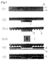
Fig. 1 shows steps of producing a printed wiring
board for use in a metal-plate-inserted ball grid array
type semiconductor plastic package in Example 1.
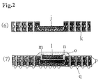
Fig. 2 shows steps of producing a printed wiring
board for use in a metal-plate-inserted ball grid array
type semiconductor plastic package in Example 1.
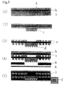
Fig. 3 shows steps of producing a printed wiring
board for use in a metal-core-inserted ball grid array type
semiconductor plastic package in Example 2.
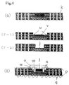
Fig. 4 shows steps of producing a printed wiring
board for use in a metal-core-inserted ball grid array type
semiconductor plastic package in Example 2.
Fig. 5 shows steps of producing a semiconductor
plastic package using a printed wiring board of the present
invention for a metal-core-inserted ball grid array.
Fig. 6 shows steps of producing a semiconductor
plastic package using a printed wiring board of the present
invention for a metal-core-inserted ball grid array.
Fig. 7 shows steps of producing a semiconductor
plastic package in Comparative Example 2.
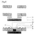
Fig. 8 shows steps of producing a semiconductor
plastic package in Comparative Example 3.
Detailed Description of the Invention
In Figures 1 to 3, reference symbols have the
following meanings, that is, a shows a metal plate, b shows
a glass fabric base material/thermosetting resin layer, c
shows an elevated portion, d shows metal protrusions having
the form of frustum of a cone each, f shows a semiconductor
chip (which is isolated from its circumferential circuit),
g shows a prepreg sheet having a hole corresponding to the
area of the metal protrusions, h shows a copper foil, i
shows a double-side copper-clad multilayer laminate, j
shows a metal exposed portion (flat portion) where a
semiconductor chip is to be mounted, k shows a through hole
for connecting circuits on front and reverse surfaces, l
shows a semiconductor chip, m shows a heat-conductive
adhesive (silver paste), n shows a bonding wire, o shows an
encapsulation resin, p shows a plating resist, q shows a
solder ball, r shows a heat-diffusing through hole, s shows
a prepreg sheet, t shows a copper plate, u shows a second-level
bonding pad, v shows a glass fabric base and a resin
layer on a metal portion on which a semiconductor chip is
to be mounted, w shows a first-level bonding pad, x shows
an etching resist, y shows an inner-layer circuit formed in
a double-side copper-clad multilayer laminate, z shows a
protective sheet made of a metal, α shows metal protrusions
having the form of frustum of a cone each, formed outside a
package, and β shows a solder ball pad.
A semiconductor plastic package is produced as
follows. A semiconductor chip is fixed on a surface of a
metal plate which surface constitutes a cavity, with a
heat-conductive adhesive such as a silver paste, the
semiconductor chip is connected by wiring bonding, then the
semiconductor chip and bonding wires are encapsulated with
a resin, and solder balls are melt-connected to a reverse
surface.
The semiconductor plastic package produced
according to the present invention is excellent in heat
conductivity, free of absorption of moisture from its lower
surface, is greatly improved in heat resistance after
moisture absorption, i.e., causes no popcorn phenomenon,
and is also suitable for mass production. There is
therefore provided semiconductor plastic packages which are
improved in economic performances and have a novel
structure. Further, the present invention uses a
polyfunctional cyanate ester composition as a thermosetting
resin, so that there can be provided semiconductor plastic
packages which are excellent in electric insulation after a
pressure cooker test and anti-migration properties and have
a novel structure.
The structure of a ball grid array type
semiconductor plastic package using the printed wiring
board produced according to the present invention will be
explained hereinafter. A metal plate is placed in a region
located as part of the thickness direction of a printed
wiring board. A region of the metal plate which region is
for mounting a semiconductor chip is flat. On the opposite
side of the printed wiring board, metal protrusions having
the form of frustum of a cone each are connected to a
copper foil forming a surface on the opposite side. The
metal plate has a size nearly equivalent to the size of
printed wiring board. The surface region of the metal
plate which surface region is for mounting a semiconductor
chip is positioned at a level lower than the level of a
circuit conductor including a peripheral bonding pad, and
the surface region constitutes a cavity and is an exposed
metal surface. At least one semiconductor chip is fixed to
the above surface region with a heat-conductive adhesive,
and the above circuit conductor and the semiconductor chip
are connected to each other by wire bonding through the
bonding pad. On the opposite side of the printed wiring
board, protrusions which have the form of frustum of a cone
each and are formed of part of the metal plate are in
contact with, and connected to, a copper foil forming the
opposite surface, and a circuit conductor pad formed for
connecting a circuit conductor formed so as to be connected
to the above metal protrusions or the package to an outside
is connected to at least the signal propagation circuit
conductor on the front surface with a through hole
conductor. And, at least the semiconductor chip, the wire
and the bonding pad are encapsulated with a resin.
In the printed wiring board according to the
present inventions 2 and 3, the bonding pad is formed at
two levels in the thickness direction, and the
semiconductor is connected to the bonding pad by wire
bonding.
The method of producing the printed wiring board
of the
present invention 1 comprises the following steps.
The method of producing a printed wiring board
having bonding pads of two levels according to the present
invention 2 will be explained below.
The method of producing a printed wiring board
according to the
present invention 2 comprises
In the present invention 1, the method of forming
a cavity portion which constitutes a semiconductor-chip-mounting
portion in the double-side copper-clad laminate is
not critical. Preferably, the cavity portion is formed by
removing copper foil on the semiconductor-chip-mounting
portion and then cutting off glass fabric base and
thermosetting resin composition by a sand blasting method.
When the printed wiring board is produced, the double-side
copper-clad laminate may have circuits formed on front and
reverse surfaces thereof in advance of the above cutting by
a sand blasting method. In this case, the circuits formed
on the front and reverse surfaces are coated with a
protective resist before the sand blasting is carried out.
When the plating with a noble metal is carried out, there
may be employed a constitution in which the entire surface
is plated with a noble metal and a portion on which the
plating is unnecessary is coated with a permanent
protective resist.
In a known method in which a semiconductor chip
is fixed on an upper surface of a metal-core-inserted
printed wiring board having a through hole, it is
inevitable to diffuse heat generated by a semiconductor
chip through a heat-diffusing through hole formed
immediately below the semiconductor memory cell chip like
heat-diffusion in a conventional P-BGA package, and a
popcorn phenomenon cannot be overcome. The present
invention employs a structure in which the through hole is
not formed below a region where a semiconductor is mounted,
so that no moisture is absorbed through the reverse surface
of the semiconductor, so that the possibility of the
popcorn phenomenon occurring is remarkably low, and there
can be provided a method of producing a semiconductor
plastic package having excellent heat diffusibility.
In the present invention 2, the method of forming
a cavity portion which constitutes a semiconductor-chip-mounting
portion in the double-side copper-clad multi-layered
board is not critical. Preferably, the cavity
portion is formed by cutting off coopper foil, glass fabric
base and thermosetting resin composition on the
semiconductor-chip-mounting portion by a sand blasting
method. First, metal foil, glass fabric base and
thermosetting resin composition on the semiconductor-chip-mounting
portion and on a region which is to constitute the
bonding pad portion of the second level are cut off by a
sand blasting method, to expose the bonding pad of the
second level. The bonding pad of the second level is
protected with a protective coating or a protective metal
so as not to be cut off, as required, and glass fabric base
and thermosetting resin composition is cut off by a sand
blasting method, or the like, until the region of the metal
plate which region is to constitute the semiconductor-chip-mounting
portion is reached and exposed. The bonding pad of
the first level and a circuit are formed on the front
surface, and on the reverse surface, the solder ball pads
for connecting the metal foil with which the metal
protrusions having the form of frustum of a cone each are
in contact to heat-diffusing solder balls and a circuit are
formed. At least the semiconductor chip, the wire bonding
pads and the solder ball pads are coated with a plating
resist, and plating with nickel and gold is carried out, to
complete the printed wiring board.
In the present invention, the method of preparing
the metal plate is not critical. For example, a metal
plate, a glass fabric base impregnated with a thermosetting
resin composition and a copper foil are laminated in this
order, to obtain a copper-clad laminate, an etching resist
is applied onto the entire surface of the laminate, the
etching resist present in a region of the exposed metal
plate surface which region is to constitute metal
protrusions having the form of frustum of a cone each and
present on the copper foil on a front surface are retained,
the rest of the etching resist is removed, and both sides
of the laminate are etched to form an elevated portion in
the region which is to constitute the metal protrusions.
The plating resist is peeled off, and then the entire
surface is coated with a plating resist. When the bonding
pad portion of the second level is required, a circuit of
the second level bonding pad is formed on the front surface.
On the reverse surface, the etching resist is retained in
the form of circles having small diameters on the elevated
portion of the metal plate and the etching resist is
retained so as to form a circuit on the other region.
Etching is carried out so as to form a circuit and metal
protrusions having the form of frustum of a cone each. The
size of the above metal protrusions is not specially
limited, while the top of each protrusion having the form
of frustum of a cone has a diameter of 0 to 1 mm, and the
bottom of each protrusion has a diameter of 0.5 to 5 mm.
The double-side metal-clad laminate having the
above metal protrusions on one surface and circuits on both
the surfaces are surface-treated by a known method as
required. The surface treatment includes oxidation
treatment, fine-roughening treatment and formation of a
coating for improving adhesion and insulation. A heat-conductive
adhesive or a solder may be applied to tops of
the above metal protrusions. On the so-treated reverse
surface of the metal plate, a glass fabric base prepreg
sheet having a hole made a little larger than the area of
the metal protrusions is placed. The glass fabric base
prepreg sheet has a thickness such that its upper surface
is on a level lower than the level of peaks of the metal
protrusions after a laminate is formed under heat and
pressure. A copper foil is placed on the glass fabric base
prepreg sheet, and the resultant set is formed into a
laminate under heat and pressure preferably in vacuum, such
that top edges of the protrusions of the metal plate cut
into the copper foil or comes in contact with the copper
foil tightly. These members are accordingly integrated to
give a double-side copper-clad multi-layered board. In
this case, it is preferred to use a glass fabric base
prepreg sheet in view of strength, while an organic base
prepreg or other prepreg may be used.
In the printed wiring board having the bonding
pad of the second level in the present invention 2, a glass
fabric base prepreg sheet having a hole made a little
larger than the area of the metal protrusions having the
form of frustum of a cone each is placed on the protrusion
side of the metal plate, a metal foil is placed on the
prepreg sheet, a glass fabric base prepreg sheet is placed
on the front surface having a region where a semiconductor
chip is to be mounted, and a copper foil is placed on the
prepreg. The resultant set is formed into a laminate under
heat and pressure preferably in vacuum, such that top edges
of the protrusions of the metal plate cut into the copper
foil or comes in contact with the copper foil tightly.
These members are accordingly integrated to give a double-side
metal-clad multi-layered board.
When a penetration hole for a through hole is
made in the above double-side copper-clad multi-layered
board with a mechanical drill or a laser, and when the
region where a semiconductor chip is to be mounted is
formed so as to be isolated from a circumferential metal
foil, the penetration hole is made so as to be partly in
contact with the metal for using the circumferential metal
foil as a circuit, and the penetration hole is placed to
form a through hole. When a metal portion where a
semiconductor chip is to be mounted is connected to a
circumferential metal, the penetration hole is made so as
not be in contact with the metal, and the entire wall of
the penetration hole is plated. On the reverse surface,
preferably, ball pads are formed in a portion where the top
edges of the metal protrusions having the form of frustum
of a cone each are in contact with a copper foil forming
the outer surface or in a portion other than the above
portion. In this case, a circuit is formed on the entire
surface by a known method such that the ball pads are
connected to the copper foil on the metal protrusions with
the circuit.
On the front surface, copper foil, glass fabric
base and thermosetting resin above a region where a
semiconductor chip is to be mounted are cut off by a spot
facing method, a sand blasting method or the like until the
metal plate located as an inner layer is reached, to expose
the metal plate, whereby a cavity type base board is
obtained. Circuits are formed on the front and reverse
surfaces, and at least a bonding pad portion and a solder
ball pad portion on the front and reverse surfaces are
coated with a plating resist. Nickel and gold plating is
carried out, to obtain a printed wiring board. When the
printed wiring board is produced, the circuits may be
formed on the front and reverse surfaces prior to the
cutting with a sand blasting method. In this case, the
circuits on the front and reverse surfaces are coated with
a protective resist or a protective metal before the sand
blasting. When a noble metal plating is carried out, there
may be employed a constitution in which the entire surface
is plated with a noble metal and a portion on which the
plating is not necessary is coated with a permanent
protective coating.
In the present invention 2, on the front surface,
metal foil, glass fabric base and thermosetting resin above
a region where a semiconductor chip is to be mounted and
the wire bonding pad portion of the second level are cut
off by spot facing, laser or sand blasting method until the
bonding pad of the second level is exposed, and then a
remainder on the region where a semiconductor chip is to be
mounted is cut off until the metal plate located as an
inner layer is reached, to expose the metal plate, whereby
a base board having a semiconductor-chip-mounting portion
formed in the form of a cavity is produced. In this case,
the bonding pad of the second level is prepared preferably
by a sand blasting method in view of accuracy.
Then, a semiconductor chip is fixed to the
semiconductor-chip-mounting portion on the front surface
with a heat-conductive adhesive, followed by wire bonding
and encapsulation with a resin. On the reverse surface,
solder balls are melted and connected, whereby a
semiconductor plastic package is obtained. The solder ball
pad portion of the reverse surface is connected to a mother
board printed wiring board with the solder balls.
Heat generated from the semiconductor chip is
thermally conducted from the semiconductor-chip-mounting
portion to the solder ball pads through the protrusions of
the metal plate and diffused into the mother board printed
wiring board which is connected to the solder ball pads
with the solder balls.
Side surfaces of the meal plate may have any
structure, such as a structure in which they are filled
with a thermosetting resin composition or they are exposed.
In view of prevention of rust, the side surfaces are
preferably filled with a thermosetting resin composition.
A hole for a through hole for connecting the
circuits on the front and reverse surfaces is made nearly
in the center of a resin-filled clearance hole or slit of
the metal plate so as not to be in contact with the metal
plate when the semiconductor-chip-mounting portion of the
metal plate is in contact with a circumferential metal
plate. The wall of the hole is plated to form a metal
layer by electroless plating or electric plating, to form a
plated through hole. In a structure where the
semiconductor-chip-mounting portion and the circumferential
metal plate are isolated from each other, the
circumferential metal plate can be used as a circuit, so
that the through hole is made so as connect the circuit.
The sand blasting method may be any generally
known sand blasting method. Specifically, it includes a
dry type air blasting method, a shot blasting method and a
wet type wet blasting method. A powder used in the above
method is selected as required. Preferably, a known powder
such as silica sand or glass powder having a size of 20 µm
or less can be used. The pressure therefor is not critical,
and the sand blasting is carried out generally at 0.1 to
0.5 MPa.
After the circuits on the front and reverse
surfaces are formed, a noble metal plating is formed at
least on the surfaces of the semiconductor-chip-mounting
portion, the bonding pad portion and the solder ball pad
portion, whereby the printed wiring board is completed. In
this case, a portion where no noble metal plating is
required is coated with a plating resist beforehand.
Otherwise, after the plating is carried out, a coating is
formed on a surface other than the surfaces of the
semiconductor-chip-mounting portion, the bonding pad
portion and the solder ball pad portion.
When the wire bonding is carried out, a
semiconductor chip is fixed to the flat metal plate as an
inner layer of the printed wiring board with a heat-conductive
adhesive, the semiconductor chip and the bonding
pad of circuit of the printed wiring board are connected by
a wire bonding method, and at least the semiconductor chip,
the bonding wire and the bonding pad are encapsulated with
a known sealing resin. In the present invention 2, the
semiconductor chip and the bonding pads of the first and
second levels are connected by a wire bonding method.
Solder balls are connected to the conductor pad
for connecting solder balls on the reverse surface opposite
to the surface where the semiconductor chip is mounted,
whereby P-BGA is obtained. The solder balls are brought
into contact with a circuit of a mother board printed
wiring board and melted by heat to be connected to the
circuit. In PLGA, a conductor pad formed on the surface of
a mother board printed wiring board for connecting solder
balls and a conductor pad for solder balls for P-LGA are
connected to each other by melting the solder balls.
The metal plate (also referred to as "metal foil"
or "copper foil") used in the present invention is not
specially limited, while the metal plate has a high elastic
modulus and high heat conductivity, and the thickness of
the metal plate is preferably 100 to 400 µm, more
preferably 5 to 200 µm. Specifically, preferred is pure
copper, oxygen-free copper or an alloy of copper with any
one of Fe, Sn, P, Cr, Zr, Zn or the like. An alloy plated
with copper may be also used. Generally, a known copper
foil is used as such. Preferably, as a copper foil, an
electrolytic copper foil having a thickness of 3 to 18 µm
is used.
The height of the metal protrusions having the
form of frustum of a cone each is not critical. Preferably,
the metal protrusions have a height hither than the level
of the surface of the metal plate as a base by 50 to 150 µm.
Further, the thickness of an insulation layer such as a
prepreg sheet is slightly smaller than the height of the
above metal protrusions after a laminate is formed under
heat and pressure, and the above thickness is preferably
smaller by 5 to 10 µm. After the laminate is formed under
heat and pressure, a resin is filled among the metal
protrusions, among lines of a circuit and in the clearance
hole or slit. Top edges of the above metal protrusions are
at least in contact with, and connected to, part of a
copper foil forming an outer layer.
The region where the metal protrusions having the
form of frustum of a cone each is formed has an area
approximately equivalent to the area of a semiconductor
chip, and generally, the region has an area of 5 x 20 mm or
smaller. Preferably, the ball pads are formed where the
copper foil is not in contact with the metal protrusions of
the metal plate reverse surface, and the ball pads are
connected to the metal foil on the protrusions with a
circuit, whereby the adhesion strength between the ball pad
portion and the board can be retained and the peel strength
(ball shear strength) when a force is laterally exerted on
the balls can be retained.
The resin for the thermosetting resin composition
used in the present invention can be selected from
generally known thermosetting resins. Specifically, the
resin includes an epoxy resin, a polyfunctional cyanate
ester resin, a polyfunctional maleimide-cyanate ester resin,
a polyfunctional maleimide resin and an unsaturated-group-containing
polyphenylene ether resin. These resins may be
used alone or in combination. In view of heat resistance,
humidity resistance, anti-migration properties and electric
properties after moisture absorption, a polyfunctional
cyanate ester resin compound is preferred.
The polyfunctional cyanate ester compound which
is a preferred thermosetting resin component in the present
invention refers to a compound having a molecule containing
at least two cyanato groups. Specific examples of the
cyanate ester compound include 1,3- or 1,4-dicyanatobenzene,
1,3,5-tricyanotobenzene, 1,3-, 1,4-, 1,6-, 1,8-, 2,6- or
2,7-dicyanatonaphthalene, 1,3,6-tricyanatonaphthalene,
4,4'-dicyanatobiphenyl, bis(4-dicyanatophenyl)methane, 2,2-bis(4-cyanatophenyl)propane,
2,2-bis(3,5-dibromo-4-cyanatophenyl)propane,
bis(4-cyanatophenyl)ether, bis (4-cyanatophenyl)thioether,
bis(4-cyanotophenyl)sulfone,
tris(4-cyanatophenyl)phosphite, tris(4-cyanatophenyl)phosphate
and cyanates obtained by a reaction
between novolak and cyan halide.
Further, there may be used polyfunctional cyanate
ester compounds disclosed in Japanese Patent Publications
Nos. 41-1928, 43-18468, 44-4791, 45-11712, 46-41112 and 47-26853
and JP-A-51-63149. Further, there may be used a
prepolymer having a molecular weight of 400 to 6,000 and
having a triazine ring formed by dimerizing cyanate groups
of any one of these polyfunctional cyanate ester compounds.
The above prepolymer can be obtained by polymerizing the
above polyfunctional cyanate ester monomer in the presence
of a catalyst selected from acids such as mineral acid and
Lewis acid, bases such as sodium alcoholate and tertiary
amines, or salts such as sodium carbonate. The prepolymer
partially contains unreacted monomer and has the form of a
mixture of a monomer and a prepolymer, and the prepolymer
in the above form is also suitably used in the present
invention. Generally, the prepolymer is used in the form a
solution thereof in an organic solvent in which it is
soluble.
The epoxy resin can be selected from generally
known epoxy resins. Specific examples thereof include a
liquid or solid bisphenol A type epoxy resin, a bisphenol F
type epoxy resin, a phenol novolak type epoxy resin, a
cresol novolak type epoxy resin, an alicyclic epoxy resin;
a polyepoxy compound obtained by epoxidizing the double
bond of butadiene, pentadiene, vinylcyclohexene or
dicyclopentyl ether; a polyol, and a polyglycidyl compound
obtained by a reaction between a hydroxyl-group-containing
silicone resin and epohalohydrin. These resins may be used
alone or in combination.
The polyimide resin is generally selected from
known polyimide resins. Specifically, it is selected from
reaction products from polyfunctional maleimides and
polyamines, and particularly from, polyimides having
terminal triple bonds, disclosed in JP-B-57-005406.
The above thermosetting resins may be used alone,
while it is preferred to use them in combination as
required in view of the balance of properties.
Various additives may be incorporated into the
thermosetting resin composition in the present invention so
long as the inherent properties of the composition are not
impaired. The above additives include monomers having
polymerizable double bonds such as unsaturated polyester,
prepolymers of these; liquid elastic rubbers having a low
molecular weight or elastic rubbers having a high molecular
weight such as polybutadiene, epoxidized butadiene,
maleated butadiene, a butadiene-acrylonitrile copolymer,
polychloroprene, a butadiene-styrene copolymer, polyisprene,
butyl rubber, fluorine rubber and natural rubber;
polyethylene, polypropylene, polybutene, poly-4-methylpentene,
polystyrene, AS resin, ABS resin, MBS resin,
styrene-isoprene rubber, a polyethylene-propylene copolymer,
a 4-fluoroethylene-6-fluoroethylene copolymer; high-molecular-weight
prepolymers or oligomers such as
polycarbonate, polyphenylene ether, polysulfone, polyester
and polyphenylene sulfide; and polyurethane. These
additives are used as required. Further, various known
additives such as an inorganic or organic filler, a dye, a
pigment, a thickener, a lubricant, an anti-foamer, a
dispersing agent, a leveling agent, a photo-sensitizer, a
flame retardant, a brightener, a polymerization inhibitor
and a thixotropic agent may be used alone or in combination
as required. A curing agent or a catalyst is incorporated
into a compound having a reactive group as required.
The thermosetting resin composition used in the
present invention undergoes curing itself under heat.
However, when it is poor in workability and economic
performances, etc., due to its low curing rate, a known
heat-curing catalyst is incorporated into the thermosetting
resin. The amount of the catalyst per 100 parts by weight
of the thermosetting resin is 0.005 to 10 parts by weight,
preferably 0.01 to 5 parts by weight.
The glass fabric base material used as a
reinforcement for the prepreg is selected from generally
known woven and non-woven fabrics, while a woven fabric is
preferred in view of a strength. Specifically, it is
selected from a know glass fiber fabric of E glass, S glass,
D glass or the like. These fabrics may be a fabric
obtained by intertwining different glass fibers. Further,
an organic base material may be used, and it is selected
from a generally known woven or non-woven fabric of a
liquid crystal polymer fiber or an wholly aromatic
polyamide fiber.
The diameter of the clearance hole or the width
of the slit made in the metal plate is a little larger than
the diameter of the through hole for conduction between the
front and reverse surfaces. Specifically, the wall of the
through hole is preferably insulated with the thermosetting
resin composition so as to have a distance of at least 50
µm from the wall of the clearance hole or the slit made in
the metal plate. Although not specially limited, the
diameter of the through hole for conduction between the
front and reverse surfaces is preferably 50 to 300 µm.
When the prepreg for the printed wiring board of
the present invention is prepared, the base material is
impregnated with the thermosetting resin composition, and
the thermosetting resin composition is dried to obtain a
semi-cured laminating material. A semi-cured resin layer
of the prepreg is formed generally at 100 to 180°C, and the
time period is 5 to 60 minutes. These conditions are
properly selected depending upon an intended flow degree.
In the
present invention 1, the method of
preparing the metal plate and the method of producing the
printed wiring board having the metal plate, for a
semiconductor plastic package, are not specially limited.
For example, the above metal plate and the printed wiring
board are produced, for example, by the following method
(Figs. 1 and 2).
When a metal foil portion where the metal
protrusions are present is viewed from below, the
semiconductor-chip-mounting portion which is present in the
central area and has the metal protrusions on the reverse
surface has a form (3-2; f) in which it is isolated from
metal foil having a circumferential circuit formed thereon.
In the
present invention 2, the method of
preparing the metal plate and the method of producing the
printed wiring board having the metal plate, for a
semiconductor plastic package, are modified.
For example, the above metal plate and the printed wiring
board are produced, for example, by the following method
(Figs. 3 and 4).
A portion which is different from any of the
exposed metal surface which constitutes the semiconductor-chip-mounting
portion and has the form of a cavity, the
bonding pad portions of the first and second levels and the
solder ball pad portion on the reverse surface is coated
with a plating resist (p), and nickel plating and gold
plating are carried out, to obtain a printed wiring board.
A semiconductor chip (l) is fixed on the semiconductor-chip-mounting
portion (j) formed of the exposed surface of
the metal plate with a heat-conductive adhesive, connected
with a bonding wire (n) and encapsulated with a resin (o),
and solder balls (q) are bonded and fixed to the solder
ball pads by melting them, to give a semiconductor plastic
package.
According to the present invention, there is
provided a method of producing a printed wiring board
having a novel structure for a semiconductor plastic
package, which is excellent in strength of adhesion to
solder balls, which is free of moisture absorption from the
lower surface of a semiconductor chip, which is greatly
improved in heat resistance after moisture absorption, i.e.,
does not cause a popcorn phenomenon, and which is suitable
for mass production and improved in economic performances.
Further, there is also provided a method of producing a
printed wiring board for a semiconductor plastic package,
which is excellent in insulation properties after pressure
cooker treatment and anti-migration properties.
Examples
The present invention will be explained more in
detail with reference to Examples hereinafter, in which
"part" stands for "part by weight" unless otherwise
specified.
Example 1
900 Parts of 2,2-bis(4-cyanatophenyl)propane and
100 parts of bis(4-maleimidophenyl methane) were melted to
150°C and allowed to react for 4 hours with stirring, to
give a prepolymer. The prepolymer was dissolved in mixed
solvents of methyl ethyl ketone and dimethylformamide. To
the resultant mixture were added 400 parts of a bisphenol A
type epoxy resin (trade name: Epikote 1001, supplied by
Yuka-Shell Epoxy K.K.) and 600 parts of a cresol novolak
type epoxy resin (trade name: ESCN-220F, supplied by
Sumitomo Chemical Industry Co., Ltd.), and these materials
were homogeneously dissolved and mixed. Further, as a
catalyst, 0.4 part of zinc octylate was added, dissolved
and mixed. To the resultant mixture were added 500 parts
of an inorganic filler (trade name: Calcined Talc, supplied
by Nippon Talc K.K.), and these materials were
homogeneously stirred and mixed to prepare a varnish A. A
50 µm thick glass woven fabric was impregnated with the
above varnish, and the impregnated glass woven fabric was
dried to prepare a semi-cured prepreg (prepreg B) having a
gelation time of 50 seconds (at 170°C) and having a resin
flow of 8 mm at 170°C at 20 kgf/cm2 for 5 minutes. The
prepreg B had an insulation layer thickness of 88 µm.
A 18 µm thick electrolytic copper foil was placed
on one surface of a sheet of the above prepreg B, a 105 µm
thick electrolytic copper foil was placed on the other
surface, and the resultant set was formed into a laminate
at 200°C at 20 kgf/cm2 for 2 hours, to give a double-side
copper-clad laminate. The entire surface of the laminate
was coated with an etching resist having a thickness of 25
µm, etching resist on the entire surface of the 18 µm thick
copper foil was retained, and on the 105 µm thick copper
foil side, etching resist was retained so as to cover an
area where an elevated portion was to be formed. Etching
was carried out to give a double-side copper clad-laminate
having an elevated portion (c) on one surface (Fig. 1-(2)).
The retained resist was removed, the entire surface was
coated with a liquid etching resist having a thickness of
25 µm, 400 resist circles having a diameter of 250 µm were
retained on the elevated portion opposite to a 15 x 15 mm
square area which was to be located in a central area of a
50 x 50 mm package area and which was to constitute a
semiconductor-chip-mounting portion, resist was retained in
a circumferential area around the elevated portion, and
etching was carried out to form 400 protrusions (d) having
the form of frustum of a cone each and a circuit (e) in an
circumferential area (Fig. 1-(3-1)). Each protrusion had a
height of 85 µm from the base copper foil surface, a bottom
side diameter of 507 µm and a top side diameter of 108 µm.
A copper foil portion which was to constitute a
semiconductor-chip-mounting portion having the protrusions
on its reverse surface had a structure (f) where it was
isolated from a copper foil for forming a circumferential
circuit.
The copper foil surface of the laminate was
oxidation-treated to form a black copper oxide, and then
one sheet of the above prepreg B (g) was placed on the
reverse surface. The above prepreg B sheet had a hole
which corresponded to an area of the metal protrusions and
had an area little larger the area of the metal protrusions.
A 18 µm thick electrolytic copper foil (h) was placed on
the prepreg B sheet, and the resultant set was formed into
a laminate and integrated, to give a double-side copper-clad
multi-layered board (i).
Through holes having a diameter of 0.25 µm each
were made with a mechanical drill, and after desmear
treatment, the entire surface was copper-plated to form a
20 µm thick copper layer by electroless plating and
electrolytic plating, whereby through hole conductors (k)
were formed. Copper foil on the semiconductor-chip-mounting
portion was removed by etching, and glass fabric
base material and thermosetting resin composition were cut
off from the front surface by a sand blasting method until
a metal surface was reached. Sand used with the blasting
method was removed through a soft etching step, and then,
circuits were formed on the front and reverse surfaces.
Solder ball pads on the reverse surface were formed so as
not to overlap with the peaks of the metal protrusions. A
plating resist (p) was formed on a portion which was not
any of the semiconductor-chip-mounting portion, the wire
bonding portion and ball pad portion on the reverse surface,
and nickel plating and gold plating were carried out, to
complete a printed wiring board. A semiconductor chip
having a size of 13 x 13 mm was fixed to the flat inner
layer metal plate portion which was the semiconductor chip
mounting portion on the front surface, with a silver paste
(m), and wire bonding was carried out. Then, the
semiconductor chip (l), a wire (n) and the bonding pads
were encapsulated with a resin, and solder balls (q) were
bonded to the reverse surfaces, to complete a semiconductor
plastic package. The semiconductor plastic package was
connected to an epoxy resin mother board printed wiring
board by melting the solder balls. Tables 1 and 2 show
evaluation results.
Comparative Example 1
Two sheets of the prepreg B obtained in Example 1
were used as a laminate. A 12 µm thick electrolytic copper
foil was placed on one surface of the laminate, and 12 µm
thick electrolytic copper foil was also placed on the other
surface. The resultant set was formed into a laminate at
200°C at 20 kgf/cm2 under a vacuum of 30 mmHg or less, to
give a double-side copper-clad laminate. Through holes
having a diameter of 0.25 mm were made in predetermined
positions with a drill, and after desmear treatment, copper
plating was carried out. Circuits were formed on the front
and reverse surfaces of the laminate by a known method,
followed by coating with a plating resist and plating with
nickel and gold. The resultant board had heat-diffusing
through holes in a region where a semiconductor chip was to
be mounted. A semiconductor chip was bonded to the region
with a silver paste, followed by wire bonding and also
followed by encapsulation with an epoxy sealing compound
and connection with solder balls in the same manner as in
Example 1. The resultant package was bonded to a mother
board. Tables 1 and 2 show evaluation results.
Comparative Example 2
300 Parts of an epoxy resin (trade name: Epikote
5045, supplied by Yuka-Shell Epoxy K.K.), 700 parts of an
epoxy resin (trade name: ESCN220F, supplied by Sumitomo
Chemical Industry Co., Ltd.), 35 parts of dicyandiamide and
1 part of 2-ethyl-4-methylimidazole were dissolved in mixed
solvents of methyl ethyl ketone and dimethyl formamide. A
glass woven fabric having a thickness of 100 µm was
impregnated with the above mixture, and the impregnated
glass woven fabric was dried to obtain a no-flow prepreg
(prepreg C) having a gelation time of 10 seconds and a
resin flow of 98 µm and a high-flow prepreg (prepreg D)
having a gelation time of 150 seconds and a resin flow of
18 mm. Two sheets of the prepreg D were used, and a
double-side copper-clad laminate was prepared by laminate-formation
at 190°C at 20 kgf/cm
2 under a vacuum of 30 mmHg
or less for 2 hours. Thereafter, a printed wiring board
was prepared in the same manner as in Comparative Example 1,
a hole was made in a portion for a semiconductor-chip-mounting
portion with a spot facing machine, and a copper
plate having a thickness 200 µm and a sheet of the above
no-flow prepreg C having a central hole were laminated
thereon. The resultant set was integrated under heat and
pressure, to obtain a radiator-possessing printed wiring
board. The so-obtained printed wiring board underwent
distortion. A semiconductor chip was fixed directly to the
radiator with a silver paste, followed by wire bonding and
encapsulation with a liquid epoxy resin (Fig. 8). The
resultant package was bonded to a mother board printed
wiring board. Tables 1 and 2 show evaluation results.
| | Example | Comparative Example |
| | 1 | 1 | 2 |
| Ball shear strength (kgf) | 1.6 | - | - |
| Heat resistance A after moisture absorption |
| Normal state | No failure | No failure | No failure |
| 24 hours | No failure | No failure | No failure |
| 48 hours | No failure | No failure | No failure |
| 72 hours | No failure | No failure | No failure |
| 96 hours | No failure | No failure | Partly peeled |
| 120 hours | No failure | Partly peeled | Partly peeled |
| 144 hours | No failure | Partly peeled | Partly peeled |
| 168 hours | No failure | Partly peeled | Partly peeled |
| Heat resistance B after moisture absorption |
| Normal state | No failure | No failure | No failure |
| 24 hours | No failure | Partly peeled | Partly peeled |
| 48 hours | No failure | Largely peeled | Largely peeled |
| 72 hours | No failure | Wire broken | Wire broken |
| 96 hours | No failure | Wire broken | Wire broken |
| 120 hours | No failure | Wire broken | Wire broken |
| 144 hours | No failure | - | - |
| 168 hours | No failure | - | - |
| | Example | Comparative Example |
| | 1 | 1 | 2 |
| Insulation resistance value (Ω) after pressure cooker treatment |
| Normal state | 5 x 10¹⁴ | 1 x 10¹⁴ | 6 x 10¹⁴ |
| 200 hours | 5 x 10¹² | 4 x 10¹² | 5 x 10⁸ |
| 500 hours | 4 x 10¹¹ | 3 x 10¹¹ | < 108 |
| 700 hours | 2 x 10¹⁰ | 2 x 10¹⁰ | - |
| 1000 hours | 1 x 10¹¹ | 1 x 10¹⁰ | - |
| Anti-migration properties (Ω) |
| Normal state | 5 x 10¹³ | 5 x 10¹³ | 4 x 10¹³ |
| 200 hours | 6 x 10¹¹ | 4 x 10¹¹ | 3 x 10⁹ |
| 500 hours | 4 x 10¹¹ | 2 x 10¹¹ | < 108 |
| 700 hours | 1 x 10¹¹ | 1 x 10¹¹ | - |
| 1000 hours | 6 x 10¹⁰ | 6 x 10¹¹ | - |
| Glass transition temperature (°C) | 234 | 234 | 160 |
| Heat diffusibility (°C) | 30 | 54 | 48 |
A solder ball was bonded to a ball pad having a
diameter of 0.65 mm, and laterally pressed to be peeled off.
The ball was measured for a strength when it was peeled off.
2) Heat resistance A after moisture absorption
A printed wiring board was treated at 30°C at
60 %RH for predetermined period of time according to JEDEC
STANDARD TEST METHOD A113-A LEVEL 3 and then subjected to 3
cycles of a 220°C reflow solder test, and the board was
studied for any failure by observation of its cross section
and electric checking.
3) Heat resistance B after moisture absorption
A printed wiring board was treated at 85°C at
60 %RH for predetermined period of time (maximum 168 hours)
according to JEDEC STANDARD TEST METHOD A113-A LEVEL 2 and
then subjected to 3 cycles of a 220°C reflow solder test,
and the board was studied for any failure by observation of
its cross section and electric checking.
4) Insulation resistance value after pressure
cooker treatment
An inter-terminal comb-shaped pattern (line/space
= 70/70 µm) was formed, prepreg sheets used were placed
thereon, the resultant set was formed into a laminate, the
resultant laminate was treated at 121°C under 2 atmospheric
pressures for a predetermined period of time and then
treated at 25°C at 60 %RH for 2 hours, 500 VDC was applied,
and 60 seconds after the application, an insulation
resistance between terminals was measured.
5) Anti-migration properties
50 VDC was applied to the same test piece as that
in the above 4) at 85°C at 85 %RH, and an insulation
resistance between terminals was measured.
6) Glass transition temperature
Measured according to a DMA method.
7) Heat diffusibility
A package was bonded to an identical mother board
printed wiring board with solder balls and continuously
used for 1,000 hours, and the package was measured for a
temperature.
Example 2
A 50 µm thick glass woven fabric was impregnated
with the same varnish A as that obtained in Example 1, and
the impregnated glass woven fabric was dried so as to
obtain a semi-cured prepreg E having a gelation time of 50
seconds (at 170°C) and a resin flow of 12 mm at 170°C at 20
kgf/cm2 for 5 minutes. The prepreg E had an insulation
layer thickness of 137 µm.
A 35 µm thick electrolytic copper foil was placed
on one surface of the above prepreg E, a 165 µm thick
electrolytic copper foil was also placed on the other
surface, and the resultant set was formed into a laminate
at 200°C at 20 kgf/cm2 for 2 hours, to give a double-side
copper-clad laminate. The entire surface of the laminate
was coated with a 25 µm thick etching resist, etching
resist was retained on the entire 35 µm thick copper foil
side, and on the 165 µm thick copper foil side, etching
resist was retained so as to cover an area where
protrusions having the form of frustum of a cone were to be
formed. Etching was carried out from both the surfaces, to
give a double-side copper-clad laminate (Fig.3-(2)) having
an elevated portion (c) on one surface. The retained
resist was removed, and the entire surface was again coated
with a liquid etching resist to form a 25 µm thick etching
resist layer. Then, 225 resist circles having a diameter
of 250 µm were retained on the elevated portion opposite to
a 15 x 15 mm square area which was to be located in a
central area of a 50 x 50 mm package area and which was to
constitute a semiconductor-chip-mounting portion, and
resist was retained in a circumferential area around the
elevated portion. On the front surface, resist was
retained for forming bonding pads of a second level and a
surface-layer circuit, and etching was carried out from
both sides to form 225 protrusions (d) having the form of
frustum of a cone each and circuits (e) in circumferential
areas on the front and reverse surfaces (Fig. 1-(3)). Each
protrusion had a height of 130 µm, a bottom portion
diameter of 612 µm and a top portion diameter of 180 µm. A
copper foil portion which was to constitute a
semiconductor-chip-mounting portion having the protrusions
on its reverse surface had a structure (f) where it was
isolated from a copper foil for forming the circumferential
circuit.
The copper foil surfaces of the laminate were
oxidation-treated to form a black copper oxide, and then
one sheet of the above prepreg E (s) was placed on the
front surface side. A sheet of the above prepreg E sheet
was also placed on the reverse surface. The latter sheet
had a hole which corresponded to an area of the metal
protrusions and had an area little larger the area of the
metal protrusions. A 18 µm thick electrolytic copper foil
(h) was placed on one of the sheets of the prepreg B, a 18
µm thick electrolytic copper foil (h) was placed on the
other of the sheets of the prepreg E, and the resultant set
was similarly formed into a laminate and integrated, to
give a double-side copper-clad multi-layered board (i).
Through holes having a diameter of 0.25 µm each
were made with a mechanical drill, and after desmear
treatment, the entire surface was copper-plated to form a
20 µm thick copper layer by electroless plating and
electrolytic plating, whereby through hole conductors (k)
were formed. Circuits were formed on the front and reverse
surfaces, and at the same time, copper foil on areas which
were to constitute the semiconductor-chip-mounting portion
and bonding pads of a second level was removed by etching,
a surface which was not on a region to constitute the
semiconductor-chip-mounting portion or the bonding pads of
the second level was coated with a resist, and glass fabric
base material and thermosetting resin composition were cut
off from the front surface by a sand blasting method until
a portion which was to constitute the bonding pads of the
second level was reached. The resist was peeled off, any
surface other than the region which was to constitute the
semiconductor-chip-mounting portion was coated with a
protective resist, glass fabric base material and
thermosetting resin composition (v) were cut off by a sand
blasting method until a metal core was reached, and the
resist was peeled off. Then, sand used with the sand
blasting method was removed through a soft etching step.
Solder ball pads on the reverse surface were formed so as
not to overlap with the peaks of the metal protrusions, but
were formed so as to be connected to the copper foil on the
protrusions. A plating resist (p) was formed on a portion
which was not any of the semiconductor-chip-mounting
portion, the wire bonding portion and a ball pad portion on
the reverse surface, and nickel plating and gold plating
were carried out, to complete a printed wiring board. A
semiconductor chip having a size of 13 x 13 mm was fixed to
the flat inner-layer metal core which was the semiconductor
chip mounting portion on the front surface, with a silver
paste (m), and wire bonding on the first and second levels
was carried out. Then, the semiconductor chip (l), wires
(n) and the bonding pads (w) were encapsulated with a
silica-containing sealing liquid resin (o), and solder
balls (q) were bonded to the reverse surfaces, to complete
a semiconductor plastic package. The semiconductor plastic
package was connected to an epoxy resin mother board
printed wiring board by melting the solder balls. Tables 3
and 4 show evaluation results.
Comparative Example 3
A semiconductor plastic package was prepared in
the same manner as in Example 2 except that solder ball
pads were formed on protrusions having the form of frustum
of a cone each. Tables 3 and 4 show evaluation results.
Comparative Example 4
Two sheets of the prepreg E obtained in Example 2
were used as a laminate. A 12 µm thick electrolytic copper
foil was placed on one surface of the laminate, and a 12 µm
thick electrolytic copper foil was placed on the other
surface, and the resultant set was formed into a laminate
at 200°C at 20 kgf/cm
2 under a vacuum of 30 mmHg or less,
to give a double-side copper-clad laminate. Through holes
having a diameter of 0.25 mm were made in predetermined
positions, and after desmear treatment, copper plating was
carried out. Circuits were formed on the front and reverse
surfaces by a known method, followed by coating with a
plating resist, nickel plating and gold plating. The
resultant board had heat-diffusing through holes in a
region where a semiconductor chip was to be mounted. A
semiconductor chip was bonded to the region with a silver
paste, followed by wire bonding and encapsulation with an
epoxy sealing compound in the same manner as in Example 2.
Solder balls were connected (Fig. 8). The so-obtained
package was similarly bonded to a mother board. Tables 3
and 4 show evaluation results.
| | Example | Comparative Example |
| | 2 | 3 | 4 |
| Ball shear strength (kgf) | 1.4 | 0.9 | - |
| Heat resistance A after moisture absorption |
| Normal state | No failure | - | No failure |
| 24 hours | No failure | - | No failure |
| 48 hours | No failure | - | No failure |
| 72 hours | No failure | - | No failure |
| 96 hours | No failure | - | No failure |
| 120 hours | No failure | - | Partly peeled |
| 144 hours | No failure | - | Partly peeled |
| 168 hours | No failure | - | Partly peeled |
| Heat resistance B after moisture absorption |
| Normal state | No failure | - | No failure |
| 24 hours | No failure | - | Partly peeled |
| 48 hours | No failure | - | Largely peeled |
| 72 hours | No failure | - | Wire broken |
| 96 hours | No failure | - | Wire broken |
| 120 hours | No failure | - | Wire broken |
| 144 hours | No failure | - | - |
| 168 hours | No failure | - | - |
| | Example | Comparative Example |
| | 2 | 3 | 4 |
| Insulation resistance value (Ω) after pressure cooker treatment |
| Normal state | 5 x 10¹⁴ | - | 6 x 10¹⁴ |
| 200 hours | 7 x 10¹² | - | 5 x 10¹² |
| 500 hours | 8 x 10¹¹ | - | 4 x 10¹¹ |
| 700 hours | 3 x 10¹⁰ | - | 5 x 10¹⁰ |
| 1000 hours | 2 x 10¹⁰ | - | 2 x 10¹⁰ |
| Anti-migration properties (Ω) |
| Normal state | 5 x 10¹³ | - | 5 x 10¹³ |
| 200 hours | 6 x 10¹¹ | - | 4 x 10¹¹ |
| 500 hours | 7 x 10¹¹ | - | 5 x 10¹¹ |
| 700 hours | 2 x 10¹¹ | - | 1 x 10¹¹ |
| 1000 hours | 8 x 10¹⁰ | - | 8 x 10¹⁰ |
| Glass transition temperature (°C) | 234 | 234 | 234 |
| Heat diffusibility (°C) | 30 | | 56 |
Varnish A was prepared in the same manner as in
Example 1. A 50 µm thick glass woven fabric was
impregnated with the varnish A, and the impregnated glass
woven fabric was dried so as to attain a gelation time of
50 seconds (at 170°C) and a resin flow of 10 mm at 170°C at
20 kgf/cm2 for 5 minutes, whereby a semi-cured prepreg F
ving an insulation layer thickness of 75 µm was obtained.
Separately, there was provided a 300 µm thick
alloy plate which had contents of Cu: 99.9 %, Fe: 0.07 %
and P:0.03 % and was used as an inner-layer metal plate. A
liquid etching resist was applied to the entire surface of
the alloy plate to form a coating having a thickness of 25
µm. Then, 400 resist circles having a diameter of 250 µm
were retained on a region opposite to a 15 x 15 mm square
area which was to be located in a central area of a 50 x 50
mm package area and which was to constitute a
semiconductor-chip-mounting portion. On the front surface,
etching resist in an area where a clearance hole having a
diameter of 0.6 mm was to be made was removed, and etching
was carried out from both sides to form 400 protrusions
having the form of frustum of a cone each on the reverse
surface and a clearance hole in a circumferential area (Fig.
5 (1), (2-1)). Each protrusion had a height of 153 µm, a
bottom portion diameter of 645 µm and a top portion
diameter of 110 µm.
Separately, a 18 µm thick electrolytic copper
foil was placed on one surface of a sheet of the above
prepreg F, a 18 µm thick electrolytic copper foil was also
placed on the other surface, and the resultant set was
formed in a laminate at 200°C at 20 kgf/cm2 for 2 hours, to
obtain a double-side copper-clad laminate (i). Bonding
pads of a second level and other circuit were formed on one
surface of the laminate, and the laminate was oxidation-treated
to form a black copper oxide. The laminate was
placed on the front surface of the above metal plate such
that the circuit side faced inward. Two sheets of the
above prepreg E (g) were placed on the reverse surface of
the metal plate. These two sheets of the prepreg (E) had
holes which corresponded to an area of the metal
protrusions and had an area little larger the area of the
metal protrusions. A 18 µm thick electrolytic copper foil
was placed thereon, and the resultant set was similarly
formed and integrated into a laminate.
Through holes having a diameter of 0.25 mm were
made in a clearance hole portion with a mechanical drill,
and after desmear treatment, the entire surface was copper-plated
to form a 20 µm thick copper layer by electroless
plating and electrolytic plating (Fig. 6(5)). Copper foil
on areas which were to constitute the semiconductor-chip-mounting
portion and bonding pads of a second level was
removed by etching, and glass fabric base material and
thermosetting resin composition were cut off from the front
surface by a sand blasting method until a portion which was
to constitute the bonding pads (u) of the second level was
reached. Then, a metal protective sheet (z) was covered on
the semiconductor-chip-mounting portion, glass fabric base
material and thermosetting resin composition were again cut
off by a sand blasting method until a metal core was
reached. Then, sand used with the sand blasting method was
removed through a soft etching step, and circuits were
formed on the front and reverse surfaces. Solder ball pads
(β) on the reverse surface were formed so as not to overlap
with the peaks of the metal protrusions. A plating resist
was formed on a portion which was not any of the
semiconductor-chip-mounting portion, the wire bonding
portion and a ball pad portion on the reverse surface, and
nickel plating and gold plating were carried out, to
complete a printed wiring board. A semiconductor chip (l)
having a size of 13 x 13 mm was fixed to the flat inner-layer
metal core which was the semiconductor chip mounting
portion on the front surface, with a silver paste (r), and
the semiconductor chip was connected to the bonding pads of
the first and second levels by wire bonding. Then, the
semiconductor chip, wires and the bonding pads were
encapsulated with a silica-containing sealing liquid resin
(o), and solder balls (q) were bonded to the reverse
surfaces, to complete a semiconductor plastic package. The
semiconductor plastic package was connected to an epoxy
resin mother board printed wiring board by melting the
solder balls. Tables 5 and 6 show evaluation results.
| | Example |
| | 3 |
| Ball shear strength (kgf) | 1.6 |
| Heat resistance A after moisture absorption |
| Normal state | No failure |
| 24 hours | No failure |
| 48 hours | No failure |
| 72 hours | No failure |
| 96 hours | No failure |
| 120 hours | No failure |
| 144 hours | No failure |
| 168 hours | No failure |
| Heat resistance B after moisture absorption |
| Normal state | No failure |
| 24 hours | No failure |
| 48 hours | No failure |
| 72 hours | No failure |
| 96 hours | No failure |
| 120 hours | No failure |
| 144 hours | No failure |
| 168 hours | No failure |
| | Example |
| | 3 |
| Insulation resistance value (Ω) after pressure cooker treatment |
| Normal state | 5 x 10¹⁴ |
| 200 hours | 7 x 10¹² |
| 500 hours | 8 x 10¹¹ |
| 700 hours | 3 x 10¹⁰ |
| 1000 hours | 2 x 10¹⁰ |
| Anti-migration properties (Ω) |
| Normal state | 5 x 10¹³ |
| 200 hours | 6 x 10¹¹ |
| 500 hours | 7 x 10¹¹ |
| 700 hours | 2 x 10¹¹ |
| 1000 hours | 8 x 10¹⁰ |
| Glass transition temperature (°C) | 234 |
| Heat diffusibility (°C) | 31 |