EP1046075B1 - Anti-aliasing apparatus and methods for optical imaging - Google Patents
Anti-aliasing apparatus and methods for optical imaging Download PDFInfo
- Publication number
- EP1046075B1 EP1046075B1 EP99902067A EP99902067A EP1046075B1 EP 1046075 B1 EP1046075 B1 EP 1046075B1 EP 99902067 A EP99902067 A EP 99902067A EP 99902067 A EP99902067 A EP 99902067A EP 1046075 B1 EP1046075 B1 EP 1046075B1
- Authority
- EP
- European Patent Office
- Prior art keywords
- light
- modifying
- filter
- transmissive
- phase
- Prior art date
- Legal status (The legal status is an assumption and is not a legal conclusion. Google has not performed a legal analysis and makes no representation as to the accuracy of the status listed.)
- Expired - Lifetime
Links
- 238000000034 method Methods 0.000 title claims description 14
- 238000012634 optical imaging Methods 0.000 title description 3
- 230000003287 optical effect Effects 0.000 claims abstract description 55
- 239000000463 material Substances 0.000 claims description 19
- 238000001228 spectrum Methods 0.000 claims 2
- 238000003384 imaging method Methods 0.000 abstract description 13
- 230000009467 reduction Effects 0.000 abstract description 7
- 230000002411 adverse Effects 0.000 abstract description 4
- 230000000694 effects Effects 0.000 description 10
- 238000005070 sampling Methods 0.000 description 9
- 238000012935 Averaging Methods 0.000 description 6
- 238000005286 illumination Methods 0.000 description 6
- 230000001419 dependent effect Effects 0.000 description 5
- 239000013078 crystal Substances 0.000 description 4
- 238000013461 design Methods 0.000 description 4
- 238000001914 filtration Methods 0.000 description 4
- 235000002595 Solanum tuberosum Nutrition 0.000 description 2
- 244000061456 Solanum tuberosum Species 0.000 description 2
- 230000004075 alteration Effects 0.000 description 2
- 239000000835 fiber Substances 0.000 description 2
- 230000004048 modification Effects 0.000 description 2
- 238000012986 modification Methods 0.000 description 2
- 239000013307 optical fiber Substances 0.000 description 2
- 238000011045 prefiltration Methods 0.000 description 2
- 238000001454 recorded image Methods 0.000 description 2
- 230000001629 suppression Effects 0.000 description 2
- 238000007792 addition Methods 0.000 description 1
- 230000005540 biological transmission Effects 0.000 description 1
- 238000005266 casting Methods 0.000 description 1
- 238000004891 communication Methods 0.000 description 1
- 230000006835 compression Effects 0.000 description 1
- 238000007906 compression Methods 0.000 description 1
- 238000012938 design process Methods 0.000 description 1
- 238000001514 detection method Methods 0.000 description 1
- 238000010586 diagram Methods 0.000 description 1
- 238000007429 general method Methods 0.000 description 1
- 238000000227 grinding Methods 0.000 description 1
- 238000000465 moulding Methods 0.000 description 1
- 208000001491 myopia Diseases 0.000 description 1
- 239000005304 optical glass Substances 0.000 description 1
- 230000008569 process Effects 0.000 description 1
- 230000001902 propagating effect Effects 0.000 description 1
- 239000010453 quartz Substances 0.000 description 1
- 230000004044 response Effects 0.000 description 1
- VYPSYNLAJGMNEJ-UHFFFAOYSA-N silicon dioxide Inorganic materials O=[Si]=O VYPSYNLAJGMNEJ-UHFFFAOYSA-N 0.000 description 1
- 238000004088 simulation Methods 0.000 description 1
- 230000007480 spreading Effects 0.000 description 1
Images


Classifications
-
- G—PHYSICS
- G02—OPTICS
- G02B—OPTICAL ELEMENTS, SYSTEMS OR APPARATUS
- G02B27/00—Optical systems or apparatus not provided for by any of the groups G02B1/00 - G02B26/00, G02B30/00
- G02B27/0025—Optical systems or apparatus not provided for by any of the groups G02B1/00 - G02B26/00, G02B30/00 for optical correction, e.g. distorsion, aberration
-
- G—PHYSICS
- G02—OPTICS
- G02B—OPTICAL ELEMENTS, SYSTEMS OR APPARATUS
- G02B27/00—Optical systems or apparatus not provided for by any of the groups G02B1/00 - G02B26/00, G02B30/00
- G02B27/42—Diffraction optics, i.e. systems including a diffractive element being designed for providing a diffractive effect
- G02B27/46—Systems using spatial filters
Definitions
- the present invention relates to apparatus and methods for reducing the spatial resolution of an optical image prior to detection to reduce image aliasing.
- the lens forms an image of the object on film, where the image is recorded.
- the film is replaced by an electronic detector such as a charge coupled device (CCD) or CMOS.
- CCD charge coupled device
- CMOS complementary metal-oxide-semiconductor
- An ideal lens that has a small F-number (focal length divided by lens diameter) captures more light and produces an image with higher spatial resolution than does an ideal lens with a large F-number.
- the amount of light that is captured increases as the square of the aperture diameter, and the theoretical spatial resolution increases linearly with the aperture diameter.
- the spatial resolution of the recorded image is limited by the spatial resolution of the digital detector or the spacing of the detector elements. Consequently, increasing the aperture size increases the amount of light gathered, but does not increase the overall spatial resolution of the imaging system. In fact, rather than simply not providing more resolution, the image can become worse as the aperture size increases, once the limit of the image detector is exceeded. This is because the large lens aperture provides excess or wasted spatial resolution that causes aliasing in the recorded image.
- Aliasing occurs when the lens presents more spatial detail to the detector array than it can record.
- the spatial detail that is left over appears as incorrect, less detailed information. That is, the image has errors caused by the detailed information that is masquerading, or aliasing, as less detailed information.
- the detail limit that the detector array can handle is normally given in terms of line pairs per millimeter of resolution, or in terms of spatial frequency information in cycles per millimeter.
- a similar effect occurs in electrical communication signals which are digitized and processed by telephones or television, when higher frequency information is supplied to the system than the system is prepared to process.
- the sampling frequency should be at least twice the highest frequency component in the signal.
- a low pass or anti-aliasing filter is used to remove the high frequency data (analogous to the extra detail in an optical image) before the signal is sampled and processed.
- the first method is simply to make the lens aperture smaller. This reduces the resolution of the image, but at the cost of reducing the amount of light captured by the system.
- the exposure time or illumination level must be increased to make up for the reduction of light.
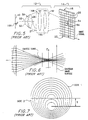
- a second method disclosed in U.S. Patent No. 2,959,105 and shown in Figures 1 and 2, teaches the use of random, coplanar spots or phase steps 2 on an optical element 1, placed near the aperture stop of the imaging system, to provide random phase noise.
- This type of system is difficult to fabricate, due to specific statistical performance required of the random phase steps.
- a similar system is described in U.S. Pat. No. 4,804,249, and shown in Figure 3, which teaches the use of a plurality of coplanar optical plateaus on an optical element, the height of any two plateaus differing by more than the coherence length of the illumination, and requires relatively broadband illumination. Such a system is difficult and expensive to fabricate.
- a third general method is to replicate the point spread function, resulting in a multiplicity of image points at the storage device for a single object point, thus spreading the light from a single object point over two or more capture elements (such as CCD elements).
- CCD elements such as CCD elements
- U.S. Patent No. 4,989,959 which teaches the use of a pyramidal structure for forming several image points for a given object point. Like any symmetrical element, this element has a misfocus component and can confuse auto-focus systems (i.e. spatial bandwidth of the combined optical/element system is dependent on focus position).
- Figure 4 illustrates this system.
- Another system of this type is disclosed in U.S. Patent No.
- Figure 9 illustrates another system of this type, which was disclosed in an article entitled "Color dependent optical prefilter for the suppression of aliasing artifacts," Applied Optics, vol. 29, no. 5 (Feb. 10, 1990) and described in U.S. Patent No. 4,575,193.
- This system utilizes a birefringent crystal (made of quartz or the like) to generate two image points for a given object point (more image points may be generated by crossing a plurality of birefringent crystals).
- the output light is polarized, limiting the application of this system. It also takes up considerable space. All of the systems of this type suffer from the same disadvantage, namely that generating several image points for each object point attenuates only a narrow range of spatial frequencies. Expanding these systems to attenuate a greater range of frequencies requires the use of increasingly complex, difficult to fabricate, and bulky elements.
- a fourth method involves placing an optical fiber bundle a specific distance from the detector array to deliberately blur the image.
- the fiber bundle must have the fibers at the output and the input arranged in exactly the same order, must be positioned accurately, and is expensive, difficult to customize, and requires considerable space.
- An example of this type of system is disclosed in U.S. Patent No. 5,299,275.
- Figure 8 shows the configuration taught in this patent.
- Element 16 uses the phase modifying characteristics of multimode optical fibers to attenuate high spatial frequency components.
- a fifth method involves deliberate use of misfocus or traditional lens aberrations to attenuate certain spatial frequencies.
- An example of this type of system is disclosed in U.S. Patent No. 5,438,366, which teaches an element which forms a disk-like image of a single point (shown in Figure 5).
- a second example of this type of system is disclosed in U.S. Patent No. 5,270,825, which teaches utilizing spherical aberration to attenuate high spatial frequencies (shown in Figure 6). Both of these systems are symmetrical, meaning they include a misfocus component which confuses auto-focus systems.
- US-A-4,642,112 discloses artificial eye lenses.
- the lenses disclosed are contact lenses and have a transmission hologram which provides diffractive power on a wavelength and/or amplitude selective basis.
- US-A-4,580,882 discloses a continuously variable contact lens.
- the concave surface thereof is disclosed as aspheric and has a desired optical power for distant viewing at the center, which increases to the desired near vision power.
- the lens also has an index of refraction.
- the present invention modifies the wavefront of light passing through it in a curved, non-symmetrical manner chosen to attenuate high spatial frequencies in the light and form a low-pass anti-aliasing filter.
- optical anti-aliasing filter of the present invention is described in claim 1.
- Dependent claims concern additional embodiments.
- Figure 10 shows a conventional imaging system comprising an object 102, a lens 104 for focussing the light from object 102, and a CCD 110 for capturing a signal representing the light from object 102 as an array of values.
- Wavefront 108 is a bowl shaped surface, concave as seen by CCD 110, formed by lens 104 as it focusses the wavefront from object 102.
- Figure 11 shows a block diagram of the anti-aliasing filter (or optical mask) 106 of the present invention in use in an optical imaging system.
- object 102 is recorded by charge coupled device (CCD) 110 via lens 106.
- Filter 106 which may be placed in front of or behind the lens, modifies the wavefront in a curved non-symmetric manner, removing the high spatial frequencies of the light and thus acting as a low pass filter. The manner of selecting an appropriate modification to be applied to the wavefront is described in detail in conjunction with Figure 26.
- filter 106 accomplishes this purpose by modifying the phase of the light passing through the filter so as to produce a curved, non-symmetrical wavefront 208 in a manner which attenuates the high spatial frequency components of the light.
- Wavefront 208 in the present example resembles a potato chip, with its near edge displaced to the right (toward CCD 110) and its back edge displaced to the left (toward filter 106).
- the potato ship shape is also somewhat bowl shaped (as in Figure 10), as the light is being focussed upon CCD 110.
- CCD 110 is used as the image recording device in the embodiments described herein, other imaging detectors, including CMOS or digital detecting means, could be used in a similar manner.
- Figure 12 shows an imaging system according to the present invention, including a reflective anti-aliasing lowpass filter 306 according to the present invention.
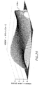
- FIG 13 shows an example 106a of transmissive anti-aliasing lowpass filter 106 of Figure 11.
- Filter 106a is a passive optical device, specifically a refraction-based optical device having curved variations in thickness (measured in the direction of the light passing through it), that when placed in the wavefront of light in an incoherent imaging system (such as that shown in Figure 10) effectively attenuates spatial frequencies to values less than some desired small level for all spatial frequencies beyond a predetermined limit.
- the predetermined limit is generally related to the maximum spatial frequency of the imaging detector (in this case CCD 110).
- the variations of thickness of the filter effect variations in the phase of the wavefront, which effect the reduction in spatial resolution of the image.
- Filter 106a might be formed of optical glass or plastic, by, for example, optical grinding, molding, casting, or compression.
- FIG 14 shows an example 306a of the reflective anti-aliasing lowpass filter 306 of Figure 12.
- Filter 306a comprises a mirrored surface that when placed in the path of the wavefront of light in an incoherent imaging system (such as that shown in Figure 10) effectively attenuates spatial frequencies to values less than some desired small level for all spatial frequencies beyond a predetermined limit.
- Wavefront 308a produced by filter 306a has the same characteristics as wavefront 208a produced by transmissive filter 106a of Figure 13.
- Figure 15 shows a second example 106b of the transmissive anti-aliasing lowpass filter 106 of Figure 11.
- filter 106b modifies the wavefront of the light from object 102 to form wavefront 208b.
- filter 106b is formed of optical material having a uniform thickness, but a spatially varying index of refraction.
- wavefront 208b has the same characteristics as wavefront 208a of Figure 13.
- Figure 16 shows a second example 306b of the reflective anti-aliasing lowpass filter 306 of Figure 12.
- Filter 306b is formed of an optical material of uniform thickness, but spatially varying index of refraction, like filter 106b of Figure 15. It further includes a reflecting back surface 320 so that light enters on the right, passes once through filter 306b, reflects off the back surface, passes a second time through filter 306b, and exits with wavefront 308b.
- the variations in the index of refraction must be chosen keeping the double path through filter 306b in mind.
- FIG 17 shows a third example 106c of the transmissive anti-aliasing lowpass filter 106 of Figure 11.
- Filter 106c comprises an array of spatial light modulators (SLMs) which affect the phase of light passing through them in such a manner as to produce desired wavefront 208c. While wavefront 208c is not curved identically to the wavefronts produced in Figures 13-16, the fact that SLM array 106c includes a great many elements makes it possible to produce an effectively curved wavefront 208c.
- SLMs spatial light modulators
- FIG 18 shows a third example 306c of the reflective anti-aliasing lowpass filter 306 of Figure 12.
- Filter 306c comprises an array of spatial light modulators (SLMs) backed by reflective surface 330.
- SLMs spatial light modulators
- the SLMs affect the phase of light passing through them in such a manner as to produce desired wavefront 308c.
- notice must be taken of the double pass through each SLM.
- wavefront 308c while not continuously curved, is effectively curved.
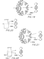
- FIG 19 shows a fourth example 106d of the transmissive anti-aliasing lowpass filter 106 of Figure 11.
- Filter 106d is a diffractive filter, formed by designing a diffractive filter such as filter 106a and then fabricating it modulo N* ⁇ , where N is an integer and ⁇ is the wavelength of the illumination. In other words, portions of the 106d filter which are above a certain height (the height being a multiple of the light wavelength) are folded back down. This results in a filter which has less thickness than the 106d filter, but which is useful for only a narrow band of light frequencies. Light passing through filter 106d forms wavefront 208d.
- FIG 20 shows a fifth example 106e of the transmissive anti-aliasing lowpass filter 106 of Figure 11.
- Filter 106e is a transmissive holographic element, designed to produce the desired wavefront 208e.
- the technique for designing transmissive holographic elements to produce any desired wavefront is well known to those skilled in the art.
- the hologram could simultaneously include the effect of lens 104, eliminating the need for that element.
- FIG 21 shows a fourth example 306d of the reflective anti-aliasing lowpass filter 306 of Figure 12.
- Filter 306d is formed by designing a reflective filter such as 306a and fabricating it modulo N* ⁇ , where N is an integer and ⁇ is the wavelength of the illumination. Light reflecting from filter 306d forms wavefront 308d.
- FIG 22 shows a fifth example 306e of reflective anti-aliasing lowpass filter 306 of Figure 12.
- Filter 306e is a reflective holographic element, designed to produce the desired wavefront 308e.
- the technique for designing reflective holographic elements to produce any desired wavefront is well known to those skilled in the art.
- the hologram could simultaneously include the effect of mirror 304, eliminating the need for that element.
- Figure 23 shows a sixth example of the transmissive anti-aliasing lowpass filter 106 of Figure 11, combining two filter elements 106f and 106g.
- Those skilled in the art will appreciate that any two or more of the foregoing transmissive or reflective elements may be combined, so long as the resulting wavefront has the desired characteristics.
- element 106f has uniform thickness and spatially varying index of refraction
- element 106g has uniform index of refraction and varying thickness.
- Light passing through both elements has wavefront 208f. Note that the features of varying thickness and varying index of refraction could also be combined in a single element.
- Figure 24 shows a sixth example of the reflective anti-aliasing lowpass filter 306 of Figure 12, combining two filter elements 306f and 306g.
- Element 306f has uniform thickness and spatially varying index of refraction, while element 306g has uniform index of refraction and varying thickness.
- Element 306f further includes a reflective back surface 331. Light passes from the right through element 306g, through element 306f, reflects off surface 331, passes back through 306f and 306g, and forms wavefront 308f.
- Figure 25 shows a seventh example of the transmissive anti-aliasing lowpass filter 106 of Figure 11, combining a filter element 106h with a lens 104b.
- Lens 104b could be in place of lens 104 in Figure 11, or both could be used.
- Filter 106h affects the phase of the light, while lens 104b focusses the light, forming wavefront 208g.
- filters described herein could also be combined with a lens, and that the lens could be refractive or diffractive.
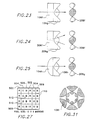
- Figure 26 shows a more detailed plot of transmissive filter 106a of Figure 13.
- the optical system includes an ideal diffraction-limited lens of focal length 11 mm with an f-number of 4.5, and the CCD 108 of Figure 2.
- the bandlimits are chosen to match the maximum spatial frequency in the vertical and horizontal direction of CCD 108.
- the constraint chosen for this example requires that the magnitude of the sampled MTF outside these spatial frequency bandlimits not exceed 15% of the maximum value of the MTF (or MTF(0,0)).
- FIG. 27 shows a specific example of a charge coupled device (CCD) array 110 for digitally recording an optical image.
- CCD charge coupled device
- This particular CCD (having 600 by 1600 video pixels) is commercially available from Polaroid, and provides a good illustration of the concepts of the present invention.
- color CCD 110 is used as an image capture device where columns of the CCD are made of contiguous pixels of the same color, with every third column having the same color.
- the required reduction in spatial resolution is different in the vertical direction than in the horizontal direction.
- Columns 502 are made of contiguous red pixels 508, columns 504 are made of contiguous green pixels 510, and columns 506 are made of contiguous blue pixels 512.
- the length of a pixel is 12 microns and the width is 6 microns.
- the fill factor in the vertical direction for each color is around 99% while the horizontal fill factor for each color is around 33%. With a fill factor of near 100 percent, sampling in the vertical direction generally describes typical grayscale image sampling. In other words, each pixel has a color filter in front of it which allows only that color of light to pass through, and active pixels are vertically adjacent. With a fill factor of 30 percent for each color, sampling in the horizontal direction generally describes typical color imager sampling, where active pixels are spatially separated.
- the goal in this example is to achieve an OTF magnitude (MTF), measured at and beyond the horizontal and vertical CCD bandlimits (27.7 Ip/mm and 41.6 Ip/mm respectively), of less than 0.15, or equivalently, the sampled spatial frequency power, IOTFI 2 , measured at and beyond the same horizontal and vertical CCD bandlimits, of less than 0.15 2 or 0.025.
- MTF OTF magnitude
- the value of the MTF at zero spatial frequency , or IH(0,0)I, is defined to be unity.
- the CCD pixels are sized 12x6 microns and arranged as shown in Figure 27.
- the design wavelength is 0.5 microns and the system F/number is F/4.5.
- phase function p(x,y) is scaled so that the maximum phase deviation is kept constant.
- phase deviation of this function is 5.7 wavelengths.
- this phase function in conjunction with the natural CCD spatial averaging for the selected detector geometry, does attenuate all spatial frequencies below the specified design limits. Very little spatial frequency power exists outside of the horizontal and vertical spatial frequency bandlimits.
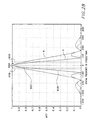
- Figures 28-30 compare the performance of the present invention to similar imaging systems utilizing no anti-aliasing measures and a prior art anti-aliasing device.
- Figure 28 shows magnitude versus spatial frequency plots for an optical imaging system like that shown in Figure 10, absent any anti-aliasing filter.
- Figure 29 shows a similar plot for the optical system utilizing a prior art anti-aliasing filter.
- Figure 30 shows magnitude versus spatial frequency plots for the optical system utilizing anti-aliasing filter 106a, shown in Figures 13 and 24.
- Figure 28 shows plots 602 and 608 of light intensity versus spatial frequency for the signal captured by CCD 110, for an idealized example of light that focusses to a small spot on one pixel.
- This is equivalent to the MTF of diffraction limited lens 104, in this example an ideal diffraction-limited lens of focal length 11 mm with an f-number of 4.5, including the spatial averaging effect of CCD 110.
- FIG. 27 shows that the horizontal spacing between identically colored pixels is three times the width of a single pixel. The vertical spacing is equal to the height of a single pixel. Therefore, the horizontal bandlimit 604 is tighter than the vertical bandlimit 606. Since there is significant MTF power outside of the needed bandlimits, a large amount of aliasing will occur if the lens/CCD combination is used as-is.
- Plot 608 shows light intensity versus vertical spatial frequency (for a vertical slice through the center of the 2-D OTF), while plot 602 is the related horizontal spatial frequency plot.
- Horizontal plot 602 is much broader than vertical plot 608, because of the combination of the lower fill factor horizontally, and the broader sampling period horizontally (refer to equation 9 for the specific relationship).
- the horizontal bandlimit 604 is tighter than the vertical bandlimit 606 because the center-to-center distance between single color pixels is greater in the horizontal direction than in the vertical direction.
- Figure 29 shows plots 612, 618 of light intensity versus spatial frequency of the signal captured by CCD 110, including the spatial averaging effect of CCD 110, for the idealized case using a prior art anti-aliasing filter (described in "Color Dependent Optical Prefilter for the Suppression of Aliasing Artifacts," by J. E. Greivenkamp, Applied Optics, Vol. 29, No. 5, 10 Feb. 1990).
- This prior art filter basically uses two of the elements shown in Figure 9, crossed to form four image point for every object point.
- This type of low pass filter approximation uses crossed birefringent crystals to, in effect, transform one ray of light propagating towards the CCD into four rays. By choosing the distance between the rays via the thickness of the crystal, various sine wave types of low pass filter approximations can be formed. The specific type used for this simulation effects a sine wave in spatial frequency with the first zero of the sine wave coinciding with the sampling frequency. This type of low pass filter still allows a considerable amount of spatial frequency power to be aliased after sampling.
- Plot 612 is the plot of intensity versus spatial frequency for the vertical direction
- plot 618 is the plot of intensity versus spatial frequency for the horizontal direction.
- Horizontal plot 508 is much broader than vertical plot 612, because of the combination of the lower fill factor horizontally, and the broader sampling period horizontally.
- the horizontal bandlimit 614 is tighter than the vertical bandlimit 616 because the center-to-center distance between single color pixels is greater in the horizontal direction than in the vertical direction.
- Figure 30 shows magnitude versus spatial frequency plots for the optical system utilizing an anti-aliasing filter according to the present invention.
- Anti-aliasing filter 106a is shown in Figure 26.
- Figure 30 shows plots 622, 628 of light intensity versus spatial frequency of the signal stored by CCD 110 (including the spatial averaging effects of CCD 110) for the idealized case of Figure 3, given anti-aliasing filter 106a of Figure 24.
- Figure 30 shows the horizontal and vertical MTFs of the example lens, including the CCD spatial averaging, after modification with anti-aliasing filter 106a. Very little spatial frequency power, when compared to Figures 28 and 29, is present outside bandlimits 624, 626.
- Figure 31 shows an eighth transmissive example 106i of the transmissive anti-aliasing lowpass filter 106 of Figure 11, for use in a system with two stopped down aperture positions.
- an anti-aliasing filter that operates at a number of discrete aperture stops is composed of a series of ring-shaped structures.
- an anti-aliasing filter that operates at full aperture and at one-half aperture is needed.
- One form of the phase function p(x,y) is: with a 1 , b 1 , a 2 , b 2 real constants.
- the constant a1 is chosen to give the desired symmetric horizontal and vertical spatial frequency bandwidths.
- the constant a2 is chosen when using the full aperture, with a1 fixed, to again give the desired spatial frequency bandwidths. This procedure can be extended to design an anti-aliasing filter that operates over any number of aperture positions.
- filter 106i comprises an inner circular portion resembling filter 106d of Figure 19, and an outer ring-shaped portion resembling a larger version of filter 106d with its center removed.
- both the top surface and the bottom surface of the filter may vary, so long as the desired phase variations on the wavefront are achieved.
- some magnitude filtering in addition to the phase filtering described herein may in some cases assist in the reduction of image spatial resolution, when the loss of light is acceptable.
Landscapes
- Physics & Mathematics (AREA)
- General Physics & Mathematics (AREA)
- Optics & Photonics (AREA)
- Transforming Light Signals Into Electric Signals (AREA)
- Microscoopes, Condenser (AREA)
- Optical Elements Other Than Lenses (AREA)
- Wire Bonding (AREA)
- Studio Devices (AREA)
- Blocking Light For Cameras (AREA)
Applications Claiming Priority (3)
| Application Number | Priority Date | Filing Date | Title |
|---|---|---|---|
| US09/005,374 US6021005A (en) | 1998-01-09 | 1998-01-09 | Anti-aliasing apparatus and methods for optical imaging |
| US5374 | 1998-01-09 | ||
| PCT/US1999/000267 WO1999035529A1 (en) | 1998-01-09 | 1999-01-06 | Anti-aliasing apparatus and methods for optical imaging |
Publications (2)
| Publication Number | Publication Date |
|---|---|
| EP1046075A1 EP1046075A1 (en) | 2000-10-25 |
| EP1046075B1 true EP1046075B1 (en) | 2002-06-05 |
Family
ID=21715527
Family Applications (1)
| Application Number | Title | Priority Date | Filing Date |
|---|---|---|---|
| EP99902067A Expired - Lifetime EP1046075B1 (en) | 1998-01-09 | 1999-01-06 | Anti-aliasing apparatus and methods for optical imaging |
Country Status (7)
| Country | Link |
|---|---|
| US (1) | US6021005A (enExample) |
| EP (1) | EP1046075B1 (enExample) |
| JP (1) | JP4384808B2 (enExample) |
| AT (1) | ATE218717T1 (enExample) |
| AU (1) | AU2213799A (enExample) |
| DE (1) | DE69901677T2 (enExample) |
| WO (1) | WO1999035529A1 (enExample) |
Cited By (3)
| Publication number | Priority date | Publication date | Assignee | Title |
|---|---|---|---|---|
| US9195074B2 (en) | 2012-04-05 | 2015-11-24 | Brien Holden Vision Institute | Lenses, devices and methods for ocular refractive error |
| US9201250B2 (en) | 2012-10-17 | 2015-12-01 | Brien Holden Vision Institute | Lenses, devices, methods and systems for refractive error |
| US9541773B2 (en) | 2012-10-17 | 2017-01-10 | Brien Holden Vision Institute | Lenses, devices, methods and systems for refractive error |
Families Citing this family (69)
| Publication number | Priority date | Publication date | Assignee | Title |
|---|---|---|---|---|
| US6911638B2 (en) | 1995-02-03 | 2005-06-28 | The Regents Of The University Of Colorado, A Body Corporate | Wavefront coding zoom lens imaging systems |
| US7218448B1 (en) | 1997-03-17 | 2007-05-15 | The Regents Of The University Of Colorado | Extended depth of field optical systems |
| US20020118457A1 (en) * | 2000-12-22 | 2002-08-29 | Dowski Edward Raymond | Wavefront coded imaging systems |
| US20020195548A1 (en) * | 2001-06-06 | 2002-12-26 | Dowski Edward Raymond | Wavefront coding interference contrast imaging systems |
| US6650476B1 (en) * | 1999-02-25 | 2003-11-18 | Lester Frank Ludwig | Image processing utilizing non-positive-definite transfer functions via fractional fourier transform |
| US7054504B2 (en) * | 1999-02-25 | 2006-05-30 | Ludwig Lester F | Relative optical path phase reconstruction in the correction of misfocused images using fractional powers of the fourier transform |
| US7039252B2 (en) * | 1999-02-25 | 2006-05-02 | Ludwig Lester F | Iterative approximation environments for modeling the evolution of an image propagating through a physical medium in restoration and other applications |
| US6536898B1 (en) * | 2000-09-15 | 2003-03-25 | The Regents Of The University Of Colorado | Extended depth of field optics for human vision |
| US7173662B1 (en) * | 2001-04-30 | 2007-02-06 | Massachusetts Institute Of Technology | Foveating imaging system and method employing a spatial light modulator to selectively modulate an input image |
| US6842297B2 (en) * | 2001-08-31 | 2005-01-11 | Cdm Optics, Inc. | Wavefront coding optics |
| AU2002357321A1 (en) * | 2001-12-18 | 2003-06-30 | University Of Rochester | Multifocal aspheric lens obtaining extended field depth |
| US20040012708A1 (en) * | 2002-07-18 | 2004-01-22 | Matherson Kevin James | Optical prefilter system that provides variable blur |
| US7031054B2 (en) | 2002-10-09 | 2006-04-18 | The Regent Of The University Of Colorado | Methods and systems for reducing depth of field of hybrid imaging systems |
| US20040174379A1 (en) * | 2003-03-03 | 2004-09-09 | Collodi David J. | Method and system for real-time anti-aliasing |
| US7180673B2 (en) | 2003-03-28 | 2007-02-20 | Cdm Optics, Inc. | Mechanically-adjustable optical phase filters for modifying depth of field, aberration-tolerance, anti-aliasing in optical systems |
| US7088419B2 (en) * | 2003-05-30 | 2006-08-08 | Cdm Optics, Inc. | Lithographic systems and methods with extended depth of focus |
| JP2007513427A (ja) | 2003-12-01 | 2007-05-24 | シーディーエム オプティックス, インコーポレイテッド | 光学システムおよびデジタルシステムの設計を最適化するシステムおよび方法 |
| US7944467B2 (en) | 2003-12-01 | 2011-05-17 | Omnivision Technologies, Inc. | Task-based imaging systems |
| US7016604B2 (en) * | 2004-06-12 | 2006-03-21 | Hewlett-Packard Development Company, L.P. | Autofocus using a holographic aperture element |
| US20070268376A1 (en) * | 2004-08-26 | 2007-11-22 | Kyocera Corporation | Imaging Apparatus and Imaging Method |
| US20060055811A1 (en) * | 2004-09-14 | 2006-03-16 | Frtiz Bernard S | Imaging system having modules with adaptive optical elements |
| US7400456B2 (en) * | 2004-09-21 | 2008-07-15 | Avago Technologies Ecbu Ip Pte Ltd | Lens having seamless profile defined by cubic polynomial function |
| US7405883B2 (en) | 2004-12-03 | 2008-07-29 | Ohara Inc. | Optical component and method of manufacture of optical component |
| JP2006311473A (ja) * | 2005-03-30 | 2006-11-09 | Kyocera Corp | 撮像装置および撮像方法 |
| US7978252B2 (en) * | 2005-03-30 | 2011-07-12 | Kyocera Corporation | Imaging apparatus, imaging system, and imaging method |
| US7616841B2 (en) * | 2005-06-17 | 2009-11-10 | Ricoh Co., Ltd. | End-to-end design of electro-optic imaging systems |
| JP4712631B2 (ja) * | 2005-07-28 | 2011-06-29 | 京セラ株式会社 | 撮像装置 |
| CN102778744A (zh) * | 2005-08-11 | 2012-11-14 | 全球仿生光学有限责任公司 | 光学透镜系统 |
| EP1927025A2 (en) | 2005-09-19 | 2008-06-04 | CDM Optics, Inc. | Task-based imaging systems |
| US8106066B2 (en) * | 2005-09-23 | 2012-01-31 | Memory Pharmaceuticals Corporation | Indazoles, benzothiazoles, benzoisothiazoles, benzisoxazoles, pyrazolopyridines, isothiazolopyridines, and preparation and uses thereof |
| US20070081224A1 (en) * | 2005-10-07 | 2007-04-12 | Robinson M D | Joint optics and image processing adjustment of electro-optic imaging systems |
| EP1954030B1 (en) * | 2005-10-18 | 2012-11-28 | Kyocera Corporation | Image pickup apparatus and image processing method |
| US20070093993A1 (en) * | 2005-10-20 | 2007-04-26 | Stork David G | End-to-end design of electro-optic imaging systems using backwards ray tracing from the detector to the source |
| CN101366270B (zh) * | 2005-11-29 | 2011-07-13 | 京瓷株式会社 | 成像设备和成像方法 |
| US8049798B2 (en) * | 2005-12-27 | 2011-11-01 | Kyocera Corporation | Imaging device and image processing method |
| US7692709B2 (en) * | 2006-05-12 | 2010-04-06 | Ricoh Co., Ltd. | End-to-end design of electro-optic imaging systems with adjustable optical cutoff frequency |
| US7889264B2 (en) * | 2006-05-12 | 2011-02-15 | Ricoh Co., Ltd. | End-to-end design of superresolution electro-optic imaging systems |
| JP2007322560A (ja) * | 2006-05-30 | 2007-12-13 | Kyocera Corp | 撮像装置、並びにその製造装置および製造方法 |
| US7924341B2 (en) * | 2006-06-05 | 2011-04-12 | Ricoh Co., Ltd. | Optical subsystem with descriptors of its image quality |
| JP4749959B2 (ja) * | 2006-07-05 | 2011-08-17 | 京セラ株式会社 | 撮像装置、並びにその製造装置および製造方法 |
| JP2008048293A (ja) * | 2006-08-18 | 2008-02-28 | Kyocera Corp | 撮像装置、およびその製造方法 |
| JP4749984B2 (ja) * | 2006-09-25 | 2011-08-17 | 京セラ株式会社 | 撮像装置、並びにその製造装置および製造方法 |
| JP4749985B2 (ja) | 2006-09-28 | 2011-08-17 | 京セラ株式会社 | 撮像装置、並びにその製造装置および製造方法 |
| WO2008081903A1 (ja) * | 2006-12-27 | 2008-07-10 | Kyocera Corporation | 撮像装置および情報コード読取装置 |
| US8567678B2 (en) * | 2007-01-30 | 2013-10-29 | Kyocera Corporation | Imaging device, method of production of imaging device, and information code-reading device |
| JP2008268937A (ja) * | 2007-03-29 | 2008-11-06 | Kyocera Corp | 撮像装置および撮像方法 |
| DE102007015599A1 (de) | 2007-03-29 | 2008-10-02 | Daimler Ag | Vermeidung von Halos um intensive Lichtquellen bei optischen Systemen, insbesondere bei Nachtsichtsystemen |
| JP2009010730A (ja) * | 2007-06-28 | 2009-01-15 | Kyocera Corp | 画像処理方法と該画像処理方法を用いた撮像装置 |
| JP4844979B2 (ja) * | 2007-08-30 | 2011-12-28 | 京セラ株式会社 | 画像処理方法と該画像処理方法を用いた撮像装置 |
| US8077401B2 (en) * | 2007-10-03 | 2011-12-13 | Ricoh Co., Ltd. | Catadioptric imaging system |
| JPWO2009069752A1 (ja) | 2007-11-29 | 2011-04-21 | 京セラ株式会社 | 撮像装置および電子機器 |
| US9865043B2 (en) | 2008-03-26 | 2018-01-09 | Ricoh Company, Ltd. | Adaptive image acquisition and display using multi-focal display |
| US9866826B2 (en) | 2014-11-25 | 2018-01-09 | Ricoh Company, Ltd. | Content-adaptive multi-focal display |
| US8897595B2 (en) * | 2008-03-26 | 2014-11-25 | Ricoh Co., Ltd. | Adaptive image acquisition for multiframe reconstruction |
| US8462213B2 (en) * | 2008-03-27 | 2013-06-11 | Kyocera Corporation | Optical system, image pickup apparatus and information code reading device |
| US8363129B2 (en) * | 2008-06-27 | 2013-01-29 | Kyocera Corporation | Imaging device with aberration control and method therefor |
| JP4658162B2 (ja) * | 2008-06-27 | 2011-03-23 | 京セラ株式会社 | 撮像装置および電子機器 |
| US7948550B2 (en) * | 2008-06-27 | 2011-05-24 | Ricoh Co., Ltd. | Electro-optic imaging system with aberrated triplet lens compensated by digital image processing |
| US8248684B2 (en) * | 2008-08-26 | 2012-08-21 | Ricoh Co., Ltd. | Control of adaptive optics based on post-processing metrics |
| US8502877B2 (en) * | 2008-08-28 | 2013-08-06 | Kyocera Corporation | Image pickup apparatus electronic device and image aberration control method |
| JP4743553B2 (ja) * | 2008-09-29 | 2011-08-10 | 京セラ株式会社 | レンズユニット、撮像装置、および電子機器 |
| US8121439B2 (en) * | 2009-05-22 | 2012-02-21 | Ricoh Co., Ltd. | End-to-end design of electro-optic imaging systems using the nonequidistant discrete Fourier transform |
| US9094656B2 (en) * | 2010-09-13 | 2015-07-28 | Thomson Licensing | Method for sequentially displaying a colour image |
| US8949078B2 (en) | 2011-03-04 | 2015-02-03 | Ricoh Co., Ltd. | Filter modules for aperture-coded, multiplexed imaging systems |
| US9219866B2 (en) | 2013-01-07 | 2015-12-22 | Ricoh Co., Ltd. | Dynamic adjustment of multimode lightfield imaging system using exposure condition and filter position |
| US9325971B2 (en) | 2013-01-10 | 2016-04-26 | The Regents Of The University Of Colorado, A Body Corporate | Engineered point spread function for simultaneous extended depth of field and 3D ranging |
| US9030580B2 (en) | 2013-09-28 | 2015-05-12 | Ricoh Company, Ltd. | Color filter modules for plenoptic XYZ imaging systems |
| US9864205B2 (en) | 2014-11-25 | 2018-01-09 | Ricoh Company, Ltd. | Multifocal display |
| DE102016112483A1 (de) | 2016-07-07 | 2018-01-11 | Connaught Electronics Ltd. | Verfahren zum Reduzieren von Störsignalen in einem Draufsichtbild, das ein Kraftfahrzeug und einen Umgebungsbereich des Kraftfahrzeugs zeigt, Fahrerassistenzsystem sowie Kraftfahrzeug |
Family Cites Families (15)
| Publication number | Priority date | Publication date | Assignee | Title |
|---|---|---|---|---|
| US2959105A (en) * | 1958-07-24 | 1960-11-08 | Canon Camera Co | Phase noise filter and its application to photography and photolithography |
| JPS57119318A (en) * | 1981-01-16 | 1982-07-24 | Minolta Camera Co Ltd | Filter having special effect |
| US4575193A (en) * | 1984-04-06 | 1986-03-11 | Eastman Kodak Company | Optical spatial frequency filter |
| US4804249A (en) * | 1986-12-24 | 1989-02-14 | Honeywell Inc. | Optical filter for incoherent imaging systems |
| US4989959A (en) * | 1989-06-12 | 1991-02-05 | Polaroid Corporation | Anti-aliasing optical system with pyramidal transparent structure |
| US5270825A (en) * | 1989-10-12 | 1993-12-14 | Olympus Optical Co., Ltd. | Imaging optical system having a moire elimination effect |
| JP2921163B2 (ja) * | 1991-04-08 | 1999-07-19 | キヤノン株式会社 | 光学的ローパスフィルターを有した撮像装置 |
| US5444574A (en) * | 1991-09-19 | 1995-08-22 | Olympus Optical Co., Ltd. | Electronic image pickup apparatus equipped with means for eliminating moire |
| US5438366A (en) * | 1993-03-31 | 1995-08-01 | Eastman Kodak Company | Aspherical blur filter for reducing artifacts in imaging apparatus |
| US5299275A (en) * | 1993-03-31 | 1994-03-29 | Eastman Kodak Company | Optical fiber filter for reducing artifacts in imaging apparatus |
| EP0618473A3 (en) * | 1993-03-31 | 1995-03-15 | Kuraray Co | Video setup with two-dimensional diffraction grating. |
| JPH06317764A (ja) * | 1993-04-27 | 1994-11-15 | Olympus Optical Co Ltd | 光学的ローパスフィルター |
| JPH09121363A (ja) * | 1995-08-17 | 1997-05-06 | Eastman Kodak Co | エイリアシングを防止するための波長選択性を有する位相型低域通過光学フィルタおよびその製造方法 |
| US5706139A (en) * | 1995-10-17 | 1998-01-06 | Kelly; Shawn L. | High fidelity optical system for electronic imaging |
| US6144493A (en) * | 1996-02-23 | 2000-11-07 | Canon Kabushiki Kaisha | Optical low-pass filter and optical apparatus having the same |
-
1998
- 1998-01-09 US US09/005,374 patent/US6021005A/en not_active Expired - Lifetime
-
1999
- 1999-01-06 DE DE69901677T patent/DE69901677T2/de not_active Expired - Lifetime
- 1999-01-06 EP EP99902067A patent/EP1046075B1/en not_active Expired - Lifetime
- 1999-01-06 WO PCT/US1999/000267 patent/WO1999035529A1/en not_active Ceased
- 1999-01-06 AT AT99902067T patent/ATE218717T1/de not_active IP Right Cessation
- 1999-01-06 JP JP2000527857A patent/JP4384808B2/ja not_active Expired - Lifetime
- 1999-01-06 AU AU22137/99A patent/AU2213799A/en not_active Abandoned
Cited By (7)
| Publication number | Priority date | Publication date | Assignee | Title |
|---|---|---|---|---|
| US9195074B2 (en) | 2012-04-05 | 2015-11-24 | Brien Holden Vision Institute | Lenses, devices and methods for ocular refractive error |
| US9535263B2 (en) | 2012-04-05 | 2017-01-03 | Brien Holden Vision Institute | Lenses, devices, methods and systems for refractive error |
| US9575334B2 (en) | 2012-04-05 | 2017-02-21 | Brien Holden Vision Institute | Lenses, devices and methods of ocular refractive error |
| US10203522B2 (en) | 2012-04-05 | 2019-02-12 | Brien Holden Vision Institute | Lenses, devices, methods and systems for refractive error |
| US10209535B2 (en) | 2012-04-05 | 2019-02-19 | Brien Holden Vision Institute | Lenses, devices and methods for ocular refractive error |
| US9201250B2 (en) | 2012-10-17 | 2015-12-01 | Brien Holden Vision Institute | Lenses, devices, methods and systems for refractive error |
| US9541773B2 (en) | 2012-10-17 | 2017-01-10 | Brien Holden Vision Institute | Lenses, devices, methods and systems for refractive error |
Also Published As
| Publication number | Publication date |
|---|---|
| DE69901677T2 (de) | 2003-01-02 |
| AU2213799A (en) | 1999-07-26 |
| ATE218717T1 (de) | 2002-06-15 |
| WO1999035529A1 (en) | 1999-07-15 |
| US6021005A (en) | 2000-02-01 |
| JP2002501216A (ja) | 2002-01-15 |
| EP1046075A1 (en) | 2000-10-25 |
| DE69901677D1 (de) | 2002-07-11 |
| JP4384808B2 (ja) | 2009-12-16 |
Similar Documents
| Publication | Publication Date | Title |
|---|---|---|
| EP1046075B1 (en) | Anti-aliasing apparatus and methods for optical imaging | |
| US6326998B1 (en) | Optical blur filter having a four-feature pattern | |
| US6525302B2 (en) | Wavefront coding phase contrast imaging systems | |
| KR100859036B1 (ko) | 촬상 시스템 및 관련 방법 | |
| US7115849B2 (en) | Wavefront coding interference contrast imaging systems | |
| JP3549898B2 (ja) | 広角の画像形成用システム及び方法 | |
| JP4652634B2 (ja) | 撮像装置 | |
| US4989959A (en) | Anti-aliasing optical system with pyramidal transparent structure | |
| US5299275A (en) | Optical fiber filter for reducing artifacts in imaging apparatus | |
| Miyata et al. | Compound-eye metasurface optics enabling a high-sensitivity, ultra-thin polarization camera | |
| US5803570A (en) | Calibration system and method for display optical systems | |
| WO2003009041A2 (en) | Wavefront coding zoom lens imaging systems | |
| EP0618470B1 (en) | Image pickup optical system | |
| US5684293A (en) | Anti-aliasing low-pass blur filter for reducing artifacts in imaging apparatus | |
| US6040857A (en) | Phase-noise type broad spectral bandwidth optical low-pass anti-aliasing filter | |
| JPH10191160A (ja) | 画像形成装置 | |
| JP3397758B2 (ja) | 撮像装置 | |
| JP3542374B2 (ja) | 撮像装置 | |
| KR100485442B1 (ko) | 일안식 입체 카메라 및 이를 이용한 입체 영상 시스템 | |
| KR100405660B1 (ko) | 텔레포토 형태의 회절광학계 | |
| JP2825860B2 (ja) | 光学的ローパスフィルター | |
| JPH10104552A (ja) | 光学的ローパスフィルター及びそれを有する光学機器 | |
| JPH02277016A (ja) | 撮像装置 | |
| Petljanski | Image improvement using dynamic optical low-pass filter | |
| JPH0492579A (ja) | 光学的ローパスフィルタ |
Legal Events
| Date | Code | Title | Description |
|---|---|---|---|
| PUAI | Public reference made under article 153(3) epc to a published international application that has entered the european phase |
Free format text: ORIGINAL CODE: 0009012 |
|
| 17P | Request for examination filed |
Effective date: 20000731 |
|
| AK | Designated contracting states |
Kind code of ref document: A1 Designated state(s): AT BE CH CY DE DK ES FI FR GB GR IE IT LI LU MC NL PT SE |
|
| 17Q | First examination report despatched |
Effective date: 20001127 |
|
| GRAG | Despatch of communication of intention to grant |
Free format text: ORIGINAL CODE: EPIDOS AGRA |
|
| GRAG | Despatch of communication of intention to grant |
Free format text: ORIGINAL CODE: EPIDOS AGRA |
|
| GRAH | Despatch of communication of intention to grant a patent |
Free format text: ORIGINAL CODE: EPIDOS IGRA |
|
| GRAH | Despatch of communication of intention to grant a patent |
Free format text: ORIGINAL CODE: EPIDOS IGRA |
|
| GRAA | (expected) grant |
Free format text: ORIGINAL CODE: 0009210 |
|
| AK | Designated contracting states |
Kind code of ref document: B1 Designated state(s): AT BE CH CY DE DK ES FI FR GB GR IE IT LI LU MC NL PT SE |
|
| PG25 | Lapsed in a contracting state [announced via postgrant information from national office to epo] |
Ref country code: NL Free format text: LAPSE BECAUSE OF FAILURE TO SUBMIT A TRANSLATION OF THE DESCRIPTION OR TO PAY THE FEE WITHIN THE PRESCRIBED TIME-LIMIT Effective date: 20020605 Ref country code: LI Free format text: LAPSE BECAUSE OF FAILURE TO SUBMIT A TRANSLATION OF THE DESCRIPTION OR TO PAY THE FEE WITHIN THE PRESCRIBED TIME-LIMIT Effective date: 20020605 Ref country code: GR Free format text: LAPSE BECAUSE OF FAILURE TO SUBMIT A TRANSLATION OF THE DESCRIPTION OR TO PAY THE FEE WITHIN THE PRESCRIBED TIME-LIMIT Effective date: 20020605 Ref country code: FI Free format text: LAPSE BECAUSE OF FAILURE TO SUBMIT A TRANSLATION OF THE DESCRIPTION OR TO PAY THE FEE WITHIN THE PRESCRIBED TIME-LIMIT Effective date: 20020605 Ref country code: CH Free format text: LAPSE BECAUSE OF FAILURE TO SUBMIT A TRANSLATION OF THE DESCRIPTION OR TO PAY THE FEE WITHIN THE PRESCRIBED TIME-LIMIT Effective date: 20020605 Ref country code: BE Free format text: LAPSE BECAUSE OF FAILURE TO SUBMIT A TRANSLATION OF THE DESCRIPTION OR TO PAY THE FEE WITHIN THE PRESCRIBED TIME-LIMIT Effective date: 20020605 Ref country code: AT Free format text: LAPSE BECAUSE OF FAILURE TO SUBMIT A TRANSLATION OF THE DESCRIPTION OR TO PAY THE FEE WITHIN THE PRESCRIBED TIME-LIMIT Effective date: 20020605 |
|
| REF | Corresponds to: |
Ref document number: 218717 Country of ref document: AT Date of ref document: 20020615 Kind code of ref document: T |
|
| REG | Reference to a national code |
Ref country code: GB Ref legal event code: FG4D |
|
| REG | Reference to a national code |
Ref country code: CH Ref legal event code: EP |
|
| REG | Reference to a national code |
Ref country code: IE Ref legal event code: FG4D |
|
| REF | Corresponds to: |
Ref document number: 69901677 Country of ref document: DE Date of ref document: 20020711 |
|
| PG25 | Lapsed in a contracting state [announced via postgrant information from national office to epo] |
Ref country code: SE Free format text: LAPSE BECAUSE OF FAILURE TO SUBMIT A TRANSLATION OF THE DESCRIPTION OR TO PAY THE FEE WITHIN THE PRESCRIBED TIME-LIMIT Effective date: 20020905 Ref country code: PT Free format text: LAPSE BECAUSE OF FAILURE TO SUBMIT A TRANSLATION OF THE DESCRIPTION OR TO PAY THE FEE WITHIN THE PRESCRIBED TIME-LIMIT Effective date: 20020905 Ref country code: DK Free format text: LAPSE BECAUSE OF FAILURE TO SUBMIT A TRANSLATION OF THE DESCRIPTION OR TO PAY THE FEE WITHIN THE PRESCRIBED TIME-LIMIT Effective date: 20020905 |
|
| ET | Fr: translation filed | ||
| NLV1 | Nl: lapsed or annulled due to failure to fulfill the requirements of art. 29p and 29m of the patents act | ||
| REG | Reference to a national code |
Ref country code: CH Ref legal event code: PL |
|
| PG25 | Lapsed in a contracting state [announced via postgrant information from national office to epo] |
Ref country code: ES Free format text: LAPSE BECAUSE OF FAILURE TO SUBMIT A TRANSLATION OF THE DESCRIPTION OR TO PAY THE FEE WITHIN THE PRESCRIBED TIME-LIMIT Effective date: 20021220 |
|
| PG25 | Lapsed in a contracting state [announced via postgrant information from national office to epo] |
Ref country code: LU Free format text: LAPSE BECAUSE OF NON-PAYMENT OF DUE FEES Effective date: 20030106 Ref country code: IE Free format text: LAPSE BECAUSE OF NON-PAYMENT OF DUE FEES Effective date: 20030106 Ref country code: CY Free format text: LAPSE BECAUSE OF FAILURE TO SUBMIT A TRANSLATION OF THE DESCRIPTION OR TO PAY THE FEE WITHIN THE PRESCRIBED TIME-LIMIT Effective date: 20030106 |
|
| PG25 | Lapsed in a contracting state [announced via postgrant information from national office to epo] |
Ref country code: MC Free format text: LAPSE BECAUSE OF NON-PAYMENT OF DUE FEES Effective date: 20030131 |
|
| REG | Reference to a national code |
Ref country code: GB Ref legal event code: 732E |
|
| PLBE | No opposition filed within time limit |
Free format text: ORIGINAL CODE: 0009261 |
|
| STAA | Information on the status of an ep patent application or granted ep patent |
Free format text: STATUS: NO OPPOSITION FILED WITHIN TIME LIMIT |
|
| 26N | No opposition filed |
Effective date: 20030306 |
|
| REG | Reference to a national code |
Ref country code: FR Ref legal event code: TP Ref country code: FR Ref legal event code: CD |
|
| REG | Reference to a national code |
Ref country code: IE Ref legal event code: MM4A |
|
| REG | Reference to a national code |
Ref country code: FR Ref legal event code: PLFP Year of fee payment: 18 |
|
| REG | Reference to a national code |
Ref country code: FR Ref legal event code: PLFP Year of fee payment: 19 |
|
| REG | Reference to a national code |
Ref country code: FR Ref legal event code: PLFP Year of fee payment: 20 |
|
| PGFP | Annual fee paid to national office [announced via postgrant information from national office to epo] |
Ref country code: FR Payment date: 20171220 Year of fee payment: 20 |
|
| PGFP | Annual fee paid to national office [announced via postgrant information from national office to epo] |
Ref country code: GB Payment date: 20171228 Year of fee payment: 20 |
|
| PGFP | Annual fee paid to national office [announced via postgrant information from national office to epo] |
Ref country code: DE Payment date: 20180109 Year of fee payment: 20 |
|
| PGFP | Annual fee paid to national office [announced via postgrant information from national office to epo] |
Ref country code: IT Payment date: 20180110 Year of fee payment: 20 |
|
| REG | Reference to a national code |
Ref country code: DE Ref legal event code: R071 Ref document number: 69901677 Country of ref document: DE |
|
| REG | Reference to a national code |
Ref country code: GB Ref legal event code: PE20 Expiry date: 20190105 |
|
| PG25 | Lapsed in a contracting state [announced via postgrant information from national office to epo] |
Ref country code: GB Free format text: LAPSE BECAUSE OF EXPIRATION OF PROTECTION Effective date: 20190105 |