EP1042820B1 - SUPRALEITERAUFBAU MIT HOCH-T c?-SUPRALEITERMATERIAL, VERFAHREN ZUR HERSTELLUNG DES AUFBAUS SOWIE STROMBEGRENZEREINRICHTUNG MIT EINEM SOLCHEN AUFBAU - Google Patents
SUPRALEITERAUFBAU MIT HOCH-T c?-SUPRALEITERMATERIAL, VERFAHREN ZUR HERSTELLUNG DES AUFBAUS SOWIE STROMBEGRENZEREINRICHTUNG MIT EINEM SOLCHEN AUFBAU Download PDFInfo
- Publication number
- EP1042820B1 EP1042820B1 EP98965108A EP98965108A EP1042820B1 EP 1042820 B1 EP1042820 B1 EP 1042820B1 EP 98965108 A EP98965108 A EP 98965108A EP 98965108 A EP98965108 A EP 98965108A EP 1042820 B1 EP1042820 B1 EP 1042820B1
- Authority
- EP
- European Patent Office
- Prior art keywords
- superconductor
- support
- layer
- interlayer
- superconducting layer
- Prior art date
- Legal status (The legal status is an assumption and is not a legal conclusion. Google has not performed a legal analysis and makes no representation as to the accuracy of the status listed.)
- Expired - Lifetime
Links
- 239000002887 superconductor Substances 0.000 title claims description 57
- 239000000463 material Substances 0.000 title claims description 45
- 238000004519 manufacturing process Methods 0.000 title description 4
- 239000010410 layer Substances 0.000 claims description 111
- 239000004020 conductor Substances 0.000 claims description 51
- 238000000034 method Methods 0.000 claims description 23
- 229910052751 metal Inorganic materials 0.000 claims description 17
- 239000002184 metal Substances 0.000 claims description 17
- 238000010276 construction Methods 0.000 claims description 15
- 239000011229 interlayer Substances 0.000 claims description 11
- 238000000151 deposition Methods 0.000 claims description 8
- 230000008021 deposition Effects 0.000 claims description 8
- 238000004804 winding Methods 0.000 claims description 7
- 229910045601 alloy Inorganic materials 0.000 claims description 5
- 239000000956 alloy Substances 0.000 claims description 5
- 238000005137 deposition process Methods 0.000 claims description 5
- 238000000608 laser ablation Methods 0.000 claims description 5
- 229910052709 silver Inorganic materials 0.000 claims description 5
- 238000007735 ion beam assisted deposition Methods 0.000 claims description 4
- 239000007769 metal material Substances 0.000 claims description 4
- 238000004544 sputter deposition Methods 0.000 claims description 4
- 229910052782 aluminium Inorganic materials 0.000 claims description 3
- QVGXLLKOCUKJST-UHFFFAOYSA-N atomic oxygen Chemical compound [O] QVGXLLKOCUKJST-UHFFFAOYSA-N 0.000 claims description 3
- 238000005229 chemical vapour deposition Methods 0.000 claims description 3
- 229910052760 oxygen Inorganic materials 0.000 claims description 3
- 239000001301 oxygen Substances 0.000 claims description 3
- 238000007650 screen-printing Methods 0.000 claims description 3
- 229910003294 NiMo Inorganic materials 0.000 claims description 2
- 229910000831 Steel Inorganic materials 0.000 claims description 2
- 239000002826 coolant Substances 0.000 claims description 2
- 239000012777 electrically insulating material Substances 0.000 claims description 2
- 239000010959 steel Substances 0.000 claims description 2
- MCMNRKCIXSYSNV-UHFFFAOYSA-N Zirconium dioxide Chemical compound O=[Zr]=O MCMNRKCIXSYSNV-UHFFFAOYSA-N 0.000 claims 2
- CETPSERCERDGAM-UHFFFAOYSA-N ceric oxide Chemical compound O=[Ce]=O CETPSERCERDGAM-UHFFFAOYSA-N 0.000 claims 1
- 229910000422 cerium(IV) oxide Inorganic materials 0.000 claims 1
- 239000000758 substrate Substances 0.000 description 7
- 230000007704 transition Effects 0.000 description 5
- 238000001816 cooling Methods 0.000 description 3
- 238000005516 engineering process Methods 0.000 description 3
- 238000001704 evaporation Methods 0.000 description 3
- 230000008020 evaporation Effects 0.000 description 3
- 229910052737 gold Inorganic materials 0.000 description 3
- 238000010438 heat treatment Methods 0.000 description 3
- 229910044991 metal oxide Inorganic materials 0.000 description 3
- 150000002739 metals Chemical class 0.000 description 3
- IJGRMHOSHXDMSA-UHFFFAOYSA-N Atomic nitrogen Chemical compound N#N IJGRMHOSHXDMSA-UHFFFAOYSA-N 0.000 description 2
- 229910004247 CaCu Inorganic materials 0.000 description 2
- 230000015556 catabolic process Effects 0.000 description 2
- 229910052802 copper Inorganic materials 0.000 description 2
- 229910000856 hastalloy Inorganic materials 0.000 description 2
- 150000002500 ions Chemical class 0.000 description 2
- -1 metal oxide compounds Chemical class 0.000 description 2
- 125000002524 organometallic group Chemical group 0.000 description 2
- 238000005240 physical vapour deposition Methods 0.000 description 2
- 238000010791 quenching Methods 0.000 description 2
- 229910052727 yttrium Inorganic materials 0.000 description 2
- VWQVUPCCIRVNHF-UHFFFAOYSA-N yttrium atom Chemical compound [Y] VWQVUPCCIRVNHF-UHFFFAOYSA-N 0.000 description 2
- 229910015901 Bi-Sr-Ca-Cu-O Inorganic materials 0.000 description 1
- 229910052684 Cerium Inorganic materials 0.000 description 1
- QPLDLSVMHZLSFG-UHFFFAOYSA-N Copper oxide Chemical compound [Cu]=O QPLDLSVMHZLSFG-UHFFFAOYSA-N 0.000 description 1
- FYYHWMGAXLPEAU-UHFFFAOYSA-N Magnesium Chemical compound [Mg] FYYHWMGAXLPEAU-UHFFFAOYSA-N 0.000 description 1
- 229910002367 SrTiO Inorganic materials 0.000 description 1
- 229910009203 Y-Ba-Cu-O Inorganic materials 0.000 description 1
- QCWXUUIWCKQGHC-UHFFFAOYSA-N Zirconium Chemical compound [Zr] QCWXUUIWCKQGHC-UHFFFAOYSA-N 0.000 description 1
- XAGFODPZIPBFFR-UHFFFAOYSA-N aluminium Chemical compound [Al] XAGFODPZIPBFFR-UHFFFAOYSA-N 0.000 description 1
- 238000004458 analytical method Methods 0.000 description 1
- 230000004323 axial length Effects 0.000 description 1
- 230000015572 biosynthetic process Effects 0.000 description 1
- 229910052797 bismuth Inorganic materials 0.000 description 1
- 239000000969 carrier Substances 0.000 description 1
- 239000000919 ceramic Substances 0.000 description 1
- ZMIGMASIKSOYAM-UHFFFAOYSA-N cerium Chemical compound [Ce][Ce][Ce][Ce][Ce][Ce][Ce][Ce][Ce][Ce][Ce][Ce][Ce][Ce][Ce][Ce][Ce][Ce][Ce][Ce][Ce][Ce][Ce][Ce][Ce][Ce][Ce][Ce][Ce][Ce][Ce][Ce][Ce][Ce][Ce][Ce][Ce][Ce] ZMIGMASIKSOYAM-UHFFFAOYSA-N 0.000 description 1
- 238000001311 chemical methods and process Methods 0.000 description 1
- 238000010549 co-Evaporation Methods 0.000 description 1
- 239000013078 crystal Substances 0.000 description 1
- 230000006378 damage Effects 0.000 description 1
- 230000001419 dependent effect Effects 0.000 description 1
- 238000007599 discharging Methods 0.000 description 1
- 238000009826 distribution Methods 0.000 description 1
- 238000010292 electrical insulation Methods 0.000 description 1
- 238000005530 etching Methods 0.000 description 1
- 238000000227 grinding Methods 0.000 description 1
- 230000017525 heat dissipation Effects 0.000 description 1
- 229910052745 lead Inorganic materials 0.000 description 1
- 239000007788 liquid Substances 0.000 description 1
- 229910052749 magnesium Inorganic materials 0.000 description 1
- 239000011777 magnesium Substances 0.000 description 1
- 238000001755 magnetron sputter deposition Methods 0.000 description 1
- 238000010297 mechanical methods and process Methods 0.000 description 1
- 150000004706 metal oxides Chemical class 0.000 description 1
- 229910052757 nitrogen Inorganic materials 0.000 description 1
- 238000013021 overheating Methods 0.000 description 1
- RVTZCBVAJQQJTK-UHFFFAOYSA-N oxygen(2-);zirconium(4+) Chemical compound [O-2].[O-2].[Zr+4] RVTZCBVAJQQJTK-UHFFFAOYSA-N 0.000 description 1
- 239000011241 protective layer Substances 0.000 description 1
- 230000000171 quenching effect Effects 0.000 description 1
- 229910052761 rare earth metal Inorganic materials 0.000 description 1
- 150000002910 rare earth metals Chemical group 0.000 description 1
- 239000007858 starting material Substances 0.000 description 1
- 229910052712 strontium Inorganic materials 0.000 description 1
- CIOAGBVUUVVLOB-UHFFFAOYSA-N strontium atom Chemical compound [Sr] CIOAGBVUUVVLOB-UHFFFAOYSA-N 0.000 description 1
- 239000000126 substance Substances 0.000 description 1
- 238000002207 thermal evaporation Methods 0.000 description 1
- 229910052726 zirconium Inorganic materials 0.000 description 1
- 229910001928 zirconium oxide Inorganic materials 0.000 description 1
Images


Classifications
-
- H—ELECTRICITY
- H10—SEMICONDUCTOR DEVICES; ELECTRIC SOLID-STATE DEVICES NOT OTHERWISE PROVIDED FOR
- H10N—ELECTRIC SOLID-STATE DEVICES NOT OTHERWISE PROVIDED FOR
- H10N60/00—Superconducting devices
- H10N60/30—Devices switchable between superconducting and normal states
-
- H—ELECTRICITY
- H02—GENERATION; CONVERSION OR DISTRIBUTION OF ELECTRIC POWER
- H02H—EMERGENCY PROTECTIVE CIRCUIT ARRANGEMENTS
- H02H9/00—Emergency protective circuit arrangements for limiting excess current or voltage without disconnection
- H02H9/02—Emergency protective circuit arrangements for limiting excess current or voltage without disconnection responsive to excess current
- H02H9/023—Current limitation using superconducting elements
-
- H—ELECTRICITY
- H01—ELECTRIC ELEMENTS
- H01F—MAGNETS; INDUCTANCES; TRANSFORMERS; SELECTION OF MATERIALS FOR THEIR MAGNETIC PROPERTIES
- H01F6/00—Superconducting magnets; Superconducting coils
- H01F2006/001—Constructive details of inductive current limiters
-
- Y—GENERAL TAGGING OF NEW TECHNOLOGICAL DEVELOPMENTS; GENERAL TAGGING OF CROSS-SECTIONAL TECHNOLOGIES SPANNING OVER SEVERAL SECTIONS OF THE IPC; TECHNICAL SUBJECTS COVERED BY FORMER USPC CROSS-REFERENCE ART COLLECTIONS [XRACs] AND DIGESTS
- Y02—TECHNOLOGIES OR APPLICATIONS FOR MITIGATION OR ADAPTATION AGAINST CLIMATE CHANGE
- Y02E—REDUCTION OF GREENHOUSE GAS [GHG] EMISSIONS, RELATED TO ENERGY GENERATION, TRANSMISSION OR DISTRIBUTION
- Y02E40/00—Technologies for an efficient electrical power generation, transmission or distribution
- Y02E40/60—Superconducting electric elements or equipment; Power systems integrating superconducting elements or equipment
-
- Y—GENERAL TAGGING OF NEW TECHNOLOGICAL DEVELOPMENTS; GENERAL TAGGING OF CROSS-SECTIONAL TECHNOLOGIES SPANNING OVER SEVERAL SECTIONS OF THE IPC; TECHNICAL SUBJECTS COVERED BY FORMER USPC CROSS-REFERENCE ART COLLECTIONS [XRACs] AND DIGESTS
- Y10—TECHNICAL SUBJECTS COVERED BY FORMER USPC
- Y10S—TECHNICAL SUBJECTS COVERED BY FORMER USPC CROSS-REFERENCE ART COLLECTIONS [XRACs] AND DIGESTS
- Y10S505/00—Superconductor technology: apparatus, material, process
- Y10S505/825—Apparatus per se, device per se, or process of making or operating same
- Y10S505/881—Resistance device responsive to magnetic field
Definitions
- the invention relates to a superconductor structure for carrying an electrical current in a predetermined direction with at least the following parts:
- the structure has a carrier made of metallic material and a conductor track located on the carrier.
- This conductor track contains at least one intermediate layer of electrically insulating material deposited on the carrier and at least one superconducting layer of a high-T c superconductor material deposited on the intermediate layer.
- the invention further relates to a method for producing a corresponding superconductor structure. Such a structure and a corresponding manufacturing process are apparent from EP 0 292 959 A.
- the invention relates to a current limiter device with such a superconductor structure.
- High-T c superconductor materials which are therefore also referred to as high-T c superconductor materials or HTS materials and, in particular, allow liquid nitrogen (LN 2 ) cooling technology.
- Such metal oxide compounds include, in particular, cuprates based on special material systems such as, for example, the types Y-Ba-Cu-O or Bi-Sr-Ca-Cu-O, where the Bi component can be partially substituted by Pb.
- Y-Ba-Cu-O or Bi-Sr-Ca-Cu-O the types Y-Ba-Cu-O or Bi-Sr-Ca-Cu-O, where the Bi component can be partially substituted by Pb.
- Several superconducting high-T c phases can occur within individual material systems, which differ in the number of copper-oxygen network planes or layers within the crystalline unit cell and which have different transition temperatures T c .
- the HTS material is generally not deposited directly on a metallic carrier tape serving as a substrate; but this carrier tape is first covered with a thin intermediate layer, which is also referred to as a buffer layer (or "buffer" layer).
- This intermediate layer with a thickness on the order of about 1 ⁇ m is intended to prevent metal atoms from diffusing into the HTS material from the substrate, which could impair the superconducting properties.
- this intermediate layer can be used to smooth the surface and improve the adhesion of the HTS material.
- Corresponding intermediate layers generally consist of oxides of metals such as zirconium, cerium, yttrium, aluminum, strontium or magnesium and are therefore electrically insulating.
- the voltage U applied at the ends drops uniformly over the entire conductor length.
- the consequence of this can be high voltage differences in the conductor track over the intermediate layer. Because of the small thickness of this layer, this inevitably leads to electrical breakdowns and thus to selective destruction of the intermediate layer and possibly the superconductor.
- a corresponding problem arises, for example, when using appropriately constructed superconductors in magnetic windings or in cables. This problem arises in particular when resistive current limiter devices are created with appropriate conductor strips. With such a device, the transition from the superconducting to the normal conducting state for current limitation in the event of a short circuit is used. It is not possible here to make the intermediate layer sufficiently voltage-resistant for the operating voltages in the kV range which are usual for such devices.
- the HTS material is applied to electrically insulating, for example ceramic, substrate plates in a known current limiter device (cf. DE 195 20 205 A ). It is also possible to deposit an additional metal layer made of an electrically highly conductive material such as Au or Ag as a shunt against burning at the so-called "hotspots" directly on the HTS material, as a result of which the HTS material is in an electrically conductive surface contact with the Metal layer is available (see DE 44 34 819 C ). The voltage problem mentioned does not exist in this case.
- the object of the present invention is in a superconductor structure with the features mentioned at the beginning of a metallic carrier the risk of unwanted Voltage differences in the conductor track over the electrical at least to reduce the insulating intermediate layer.
- This object is achieved in that between the superconducting layer of the conductor track and the carrier at least one assigned to the conductor track, in the current carrying direction extending, electrically conductive connecting part is formed with which the superconducting layer is electrically connected in parallel with the carrier.
- An embodiment of the at least one can advantageously be electrical conductive connecting part between the superconducting layer and the carrier can be provided in that in the a deposition corresponding to at least one connection area the intermediate layer avoided or the intermediate layer removed before deposition of the superconducting layer becomes. Instead, at least one can find out about the corresponding one extending at least one connection area metallic layer part are deposited.
- the superconductor structure can be advantageous produce that as a deposition process for the superconductor material simultaneous thermal evaporation of the individual Components of the superconductor material with oxygen supply, or a laser ablation procedure, or a sputtering procedure, or a chemical evaporation process, in particular with organometallic components of the superconductor material, or a screen printing process is provided.
- a deposition process for the superconductor material simultaneous thermal evaporation of the individual Components of the superconductor material with oxygen supply, or a laser ablation procedure, or a sputtering procedure, or a chemical evaporation process, in particular with organometallic components of the superconductor material, or a screen printing process is provided.
- the intermediate layer material a deposition process with ion current support (IBAD) is provided.
- IBAD ion current support
- the superconductor material then advantageously also grows biaxially textured on so that by eliminating current limiting Grain boundaries high critical current densities can be achieved.
- the superconductor structure according to the invention can be particularly advantageous provided to form a current limiter device become. Because the use of a metallic carrier for the superconductor material ensures rapid heat dissipation to the required cryogenic medium and such accordingly fast switching sequence.
- the superconductor structure according to the invention therefore comprises at least: a carrier, which can also be referred to as a substrate, and at least one conductor track located thereon.
- This conductor track comprises at least one intermediate layer deposited on the carrier, also referred to as a buffer layer, and a layer made of an HTS material applied to this intermediate layer. Both layers are structured to the ladder ban.
- a plate or a tape or other structure made of a metallic material is used with an inherently arbitrary thickness and the dimensions of its surface required for the respective application.
- All elemental metals or alloys of these metals known as carriers for HTS materials are suitable as metallic materials.
- Cu, Al or Ag or their alloys with one of the elements as the main component or steels as well as special NiMo alloys, in particular with the trade name "Hastelloy”, are suitable.
- the at least one intermediate layer should consist of a material that ensures such growth.
- An intermediate layer with a texture adapted to the crystalline dimensions of the HTS material is therefore particularly suitable.
- the interlayer material should be electrically insulating. Biaxially textured zirconium oxide stabilized with yttrium (abbreviation: "YSZ”) is advantageous.
- buffer layer materials such as CeO 2 , YSZ + CeO 2 (as a double layer), Pr 6 O 11 , MgO, YSZ + tin-doped In 2 O 3 (as a double layer), SrTiO 3 or La 1-x Ca x MnO 3 suitable.
- One or more of these materials is deposited on the surface of the carrier in a manner known per se.
- IBAD method ion B eam A ssisted D eposition method
- other methods are also suitable, such as sputtering or laser ablation at a predetermined angle.
- the intermediate layer material is deposited on the carrier at elevated temperatures.
- the layer thickness of the textured intermediate layer produced in this way is generally between 0.1 and 2 ⁇ m.
- the HTS material is then on the intermediate layer using known deposition processes while heating the Carrier generally up to a few micrometers in thickness applied.
- PVD Physical Vapor Deposition
- CVD Chemical Vapor Deposition
- a screen printing method known per se can also be provided become.
- HTS materials All known metal oxide high-T c superconductor materials which in particular permit an LN 2 cooling technology can be considered as HTS materials.
- the HTS layer can be covered with at least one further layer such as a protective layer or a layer serving as a shunt resistor.
- the intermediate layer and the HTS layer on it are structured into at least one conductor track. It can correspondingly discretely deposited layer tracks are also provided his.
- a corresponding superconductor structure according to the invention band-shaped carrier, intermediate layer and HTS layer is also the embodiment illustrated in cross section in FIG on the basis and generally designated 10.
- the carrier with 11 the intermediate layer with 12 and the HTS layer designated 13
- the intermediate layer 12 and the HTS layer 13 form a strip-shaped conductor track L.
- the HTS layer 13 and the carrier 11 of the conductor track L at least one electrically conductive Connection part to be present, which is in the by one Arrow indicated direction of an electric current I extends. That is, seen in this direction with the at least one connecting part over the entire length of the Construction either a parallel connection of the Superconducting layer can be produced with the carrier.
- two connecting parts in the form of lateral, strip-shaped layers 15a and 15b from one electrically conductive metal such as Ag, Au or Cu formed.
- one electrically conductive metal such as Ag, Au or Cu formed.
- To produce these strip-shaped metal layers 15a and 15b is in at least one of the two lateral, strip-shaped Edge regions 11a and 11b of the band-shaped carrier 11 the buffer layer 12 during deposition, for example by a Shadow mask either not applied or after by mechanical or chemical processes such as grinding, etching, Evaporation removed with a laser beam.
- the width b this now bare edge regions 11a and 11b of the carrier should advantageously be at least five times the thickness d of the HTS layer 13, preferably substantially higher are up to a hundred times.
- the contact between the HTS layer 13 and the carrier 11 then take place by application the strip-shaped metal layers 15a and 15b, the extend laterally across the intermediate layer 12 and the respective edge region of the superconductor layer and the cover bare edge areas 11a and 11b of the carrier.
- the HTS layer can be like the intermediate layer in the edge areas 11a and 11b have been removed or are beyond extend.
- the lateral extent is a of the metal layers 15a and 15b small, preferably 1/10 to 1/100, compared to the width B of the strip-shaped superconductor layer 13 or the underlying intermediate layer 12.
- the maximum thickness of these metal layers is in general at most equal to the thickness d of the HTS layer 13.
- the HTS layer 23 of its conductor track L extends laterally beyond the narrower intermediate layer 22 to the entire width of the carrier 11. Consequently, in this embodiment there are no special metal strips for contacting required, but the HTS layer is in the edge regions 11a and 11b of the carrier 11 in direct electrical contact with the carrier by overlapping the intermediate layer 22 laterally.
- the superconducting parameters such as the critical current density J c and / or the critical temperature T c in the corresponding edge strips 23 a and 23 b of the HTS layer 23 can be reduced in the vicinity of the edge of the intermediate layer 22 and on the edge regions 11 a and 11 b. If necessary, even the material of layer 13 can be normally conductive here.
- the intermediate layer 32 has one about tooth-like lateral contour, the middle tooth width w is advantageously at least 5 times the size of the thickness d of the HTS layer 33. In this way, a Extend the length of the overheating zone between superconducting material of the conductor track and the metallic Carrier can be reached, the contact resistance accordingly is reduced.
- a cross section corresponding to FIG. 4 would then also occur result when using a single conductor track on the carrier loop-shaped or U-shaped or meandering shape is trained.
- Figure 5 shows a plan view of a strip-shaped superconductor structure according to Figure 1 or Figure 2.
- the structure 20 according to FIG. 2 with conductor track L assumed.
- a portion 23t of the HTS layer indicated by shading 23 of this conductor track had become normally conductive (resistive).
- the flow of current I that then occurs is indicated by streamlines, the streamlines in the HTS layer 23 designated by i and by solid lines are illustrated while extending through the carrier extending streamlines i 'are drawn in dashed lines.
- the resistance of the resistive section 23t is large the parallel distance of the carrier belt, the largest gives way Part of the current I parallel to the former via the electrical Connection of the edge strips 23a and 23b at the edges in the metallic carrier.
- B is the width of the HTS layer.
- the metallic Carrier also acts as a shunt resistor to the superconductor and saves e.g. advantageous in a current limiter device an additional application of a low-resistance film highly conductive material such as Ag or Au on the surface of the HTS layer to prevent an inadmissible heating the superconductor path in a prematurely normal one Avoid "hotspot".
- the superconductor structure according to the invention can be provided particularly advantageously for a resistive current limiter device.
- a large-area plate-shaped structure or, as assumed below, a strip conductor type according to one of the embodiments according to FIGS. 1 and 3 is used, in which a YBa 2 Cu 3 O 7-x - on a preferably textured intermediate layer (buffer layer) of its conductor track L. Layer of about 0.3 to 10 microns thick is applied.
- the corresponding strip conductor then carries the current without resistance until the critical current J c is reached and, after becoming quenched by exceeding J c, has a sufficiently high resistance to be able to effectively limit a fault current in the event of a short circuit.
- the metal strip of the carrier acts as a shunt to the superconductor layer and limits the temperature rise in "hotspots" that have become normally conductive.
- its carrier should be as thin as possible, in particular have a thickness between 0.03 and 0.1 mm, and be made of a metal with a high specific electrical resistance, such as in particular Hastelloy.
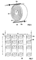
- a low-inductance, module-like limiter element 50 can advantageously be formed by parallel winding of strip conductors 20 and 20 'electrically connected to one another at a common end 51 to form a bifilar disk winding 52.
- Insulating tapes 53 for electrical insulation are inserted between adjacent tape layers of the winding 52, which, for example, by means of a corrugated or ribbed structure, at the same time facilitate the access of a coolant to the tape conductors for the purpose of rapid re-cooling after a switching operation.
- connection conductors 54a and 54b for the electrical connection of the strip conductor winding 52 or for supplying and discharging an electrical current I are also indicated.
- a current limiter device can be used build up, which is indicated in Figure 7 and designated 60 is. By connecting several of these in parallel n times Elements with nominal current I and nominal voltage U can then Current limiting devices for specific nominal currents n ⁇ I and by an m-fold series connection for nominal voltages m ⁇ U be formed.
- a current limiter device 60 according to FIG. 7 is used as the basis for the details of a specific exemplary embodiment, which are summarized below in the form of a table:
Landscapes
- Engineering & Computer Science (AREA)
- Power Engineering (AREA)
- Superconductors And Manufacturing Methods Therefor (AREA)
- Containers, Films, And Cooling For Superconductive Devices (AREA)
- Emergency Protection Circuit Devices (AREA)
Applications Claiming Priority (3)
| Application Number | Priority Date | Filing Date | Title |
|---|---|---|---|
| DE19756854 | 1997-12-19 | ||
| DE19756854 | 1997-12-19 | ||
| PCT/DE1998/003596 WO1999033122A1 (de) | 1997-12-19 | 1998-12-07 | SUPRALEITERAUFBAU MIT HOCH-Tc-SUPRALEITERMATERIAL, VERFAHREN ZUR HERSTELLUNG DES AUFBAUS SOWIE STROMBEGRENZEREINRICHTUNG MIT EINEM SOLCHEN AUFBAU |
Publications (2)
| Publication Number | Publication Date |
|---|---|
| EP1042820A1 EP1042820A1 (de) | 2000-10-11 |
| EP1042820B1 true EP1042820B1 (de) | 2003-03-12 |
Family
ID=7852730
Family Applications (1)
| Application Number | Title | Priority Date | Filing Date |
|---|---|---|---|
| EP98965108A Expired - Lifetime EP1042820B1 (de) | 1997-12-19 | 1998-12-07 | SUPRALEITERAUFBAU MIT HOCH-T c?-SUPRALEITERMATERIAL, VERFAHREN ZUR HERSTELLUNG DES AUFBAUS SOWIE STROMBEGRENZEREINRICHTUNG MIT EINEM SOLCHEN AUFBAU |
Country Status (8)
| Country | Link |
|---|---|
| US (1) | US6522236B1 (https=) |
| EP (1) | EP1042820B1 (https=) |
| JP (1) | JP4359387B2 (https=) |
| CA (1) | CA2315081A1 (https=) |
| DE (1) | DE59807505D1 (https=) |
| DK (1) | DK1042820T3 (https=) |
| NO (1) | NO20003156D0 (https=) |
| WO (1) | WO1999033122A1 (https=) |
Cited By (3)
| Publication number | Priority date | Publication date | Assignee | Title |
|---|---|---|---|---|
| EP2472618A1 (en) | 2011-01-03 | 2012-07-04 | Nexans | Superconducting resistive fault current limiter |
| EP2991126A1 (de) | 2014-08-25 | 2016-03-02 | Theva Dünnschichttechnik GmbH | Verfahren und Vorrichtung zum Herstellen eines Hochtemperatur-Supraleiters |
| DE102016206573A1 (de) * | 2016-04-19 | 2017-10-19 | Siemens Aktiengesellschaft | Elektrische Spulenwicklung |
Families Citing this family (24)
| Publication number | Priority date | Publication date | Assignee | Title |
|---|---|---|---|---|
| DE19957981A1 (de) | 1999-12-02 | 2001-06-07 | Abb Research Ltd | Hochtemperatursupraleiteranordnung und Verfahren zu deren Herstellung |
| DE10163008C5 (de) * | 2001-02-07 | 2013-04-18 | Siemens Aktiengesellschaft | Resistive Strombegrenzungseinrichtung mit mindestens einer Leiterbahn mit supraleitendem und normalleitendem Material |
| DE10134515B4 (de) * | 2001-07-16 | 2004-05-06 | W.E.T. Automotive Systems Ag | Leitereinrichtung mit einem eine Verengung aufweisenden flächigen Hauptleiter |
| DE10225935C5 (de) * | 2002-06-11 | 2011-10-06 | THEVA DüNNSCHICHTTECHNIK GMBH | Vorrichtung zum Leiten von Strom |
| DE10230083B3 (de) * | 2002-06-27 | 2004-02-05 | Siemens Ag | Strombegrenzungseinrichtung mit verbesserter Wärmeableitung |
| GB0411035D0 (en) * | 2004-05-18 | 2004-06-23 | Diboride Conductors Ltd | Croygen-free dry superconducting fault current limiter |
| WO2006001226A1 (ja) * | 2004-06-24 | 2006-01-05 | National Institute Of Advanced Industrial Science And Technology | 超電導限流素子及びその作製方法 |
| US7816303B2 (en) * | 2004-10-01 | 2010-10-19 | American Superconductor Corporation | Architecture for high temperature superconductor wire |
| DE102004048644B4 (de) * | 2004-10-04 | 2006-08-10 | Siemens Ag | Vorrichtung zur resistiven Strombegrenzung mit bandförmiger Hoch-Tc -Supraleiterbahn |
| DE102004048647B4 (de) | 2004-10-04 | 2006-08-10 | Siemens Ag | Resistive Strombegrenzereinrichtung mit bandförmiger Hoch-Tc-Supraleiterbahn |
| DE102004048648B4 (de) * | 2004-10-04 | 2006-08-10 | Siemens Ag | Vorrichtung zur Strombegrenzung vom resistiven Typ mit bandfömigem Hoch-Tc-Supraleiter |
| DE102004048646B4 (de) | 2004-10-04 | 2006-08-10 | Siemens Ag | Supraleitende Strombegrenzereinrichtung vom resistiven Typ mit bandförmiger Hoch-Tc-Supraleiterbahn |
| JP2009507358A (ja) * | 2005-07-29 | 2009-02-19 | アメリカン・スーパーコンダクター・コーポレーション | 高温超電導ワイヤ及びコイル |
| DE502006004122D1 (de) | 2006-03-02 | 2009-08-13 | Theva Duennschichttechnik Gmbh | Resistiver Strombegrenzer |
| JP4810268B2 (ja) * | 2006-03-28 | 2011-11-09 | 株式会社東芝 | 超電導線材の接続方法及び超電導線材 |
| DE102006032702B3 (de) * | 2006-07-14 | 2007-10-04 | Siemens Ag | Resistive supraleitende Strombegrenzeinrichtung mit bifilarer Spulenwicklung aus HTS-Bandleitern und Windungsabstandshalter |
| DE102006032972B3 (de) * | 2006-07-17 | 2008-02-14 | Siemens Ag | Supraleitende Strombegrenzereinrichtung vom resistiven Typ mit mehrteiligem Halteelement |
| DE102006032973B3 (de) | 2006-07-17 | 2008-02-14 | Siemens Ag | Supraleitende Strombegrenzereinrichtung von resistiven Typ mit Halteelement |
| DE102008029722B3 (de) * | 2008-06-23 | 2009-12-17 | Siemens Aktiengesellschaft | Leiteranordnung für ein resistives Schaltelement mit wenigstens zwei Leiterverbünden aus supraleitenden Leiterbändern |
| PL2302711T3 (pl) * | 2008-11-29 | 2013-05-31 | Alstom Technology Ltd | Ogranicznik prądu zakłóceniowego z wieloma nadprzewodzącymi elementami, połączonymi w kształt pierścienia |
| JP5513154B2 (ja) * | 2010-02-12 | 2014-06-04 | 昭和電線ケーブルシステム株式会社 | 酸化物超電導線材及び酸化物超電導線材の製造方法 |
| JP2012256508A (ja) * | 2011-06-08 | 2012-12-27 | Sumitomo Electric Ind Ltd | 超電導線材、および超電導ケーブル |
| JP2016152301A (ja) * | 2015-02-17 | 2016-08-22 | ローム株式会社 | チップ抵抗器およびその製造方法 |
| EP3121860B1 (de) | 2015-07-21 | 2020-11-25 | Nexans | Anordnung zur strombegrenzung in einem der stromversorgung dienenden netzwerk |
Family Cites Families (14)
| Publication number | Priority date | Publication date | Assignee | Title |
|---|---|---|---|---|
| US3098967A (en) * | 1959-01-09 | 1963-07-23 | Sylvania Electric Prod | Cryotron type switching device |
| US3296459A (en) * | 1964-01-13 | 1967-01-03 | Gen Electric | Superconductor circuit with protuberances |
| US3363211A (en) * | 1965-04-02 | 1968-01-09 | Ford Motor Co | Quantum interference device |
| US3936677A (en) * | 1975-01-21 | 1976-02-03 | Bell Telephone Laboratories, Incorporated | Supercurrent device for controlling mobile flux vortices |
| CA1326976C (en) * | 1987-05-26 | 1994-02-15 | Satoshi Takano | Superconducting member |
| SE461306B (sv) * | 1988-06-10 | 1990-01-29 | Asea Brown Boveri | Stroembegraensare |
| US5140300A (en) * | 1988-10-24 | 1992-08-18 | Sharp Kabushiki Kaisha | Superconductive magneto-resistive device comprising laminated superconductive ceramic films |
| JPH02281765A (ja) * | 1989-04-24 | 1990-11-19 | Furukawa Electric Co Ltd:The | 酸化物超電導体薄膜を用いた超電導素子 |
| US5010300A (en) * | 1989-08-11 | 1991-04-23 | Picker International, Inc. | Multi-axis pre-saturated spin echo phase encoded spectroscopy |
| DE4004908A1 (de) | 1990-02-16 | 1991-08-22 | Daimler Benz Ag | Oxidkeramische streifenleiter auf metallischen baendern |
| DE4107685A1 (de) | 1991-03-09 | 1992-09-10 | Abb Patent Gmbh | Supraleitender strombegrenzer |
| DE4119984A1 (de) * | 1991-06-18 | 1992-12-24 | Hoechst Ag | Resistiver strombegrenzer |
| JPH05163005A (ja) * | 1991-12-12 | 1993-06-29 | Mitsubishi Electric Corp | 酸化物超電導限流導体の製造方法 |
| DE19520205A1 (de) | 1995-06-01 | 1996-12-05 | Siemens Ag | Resistive Strombegrenzungseinrichtung unter Verwendung von Hoch-T¶c¶Supraleitermaterial |
-
1998
- 1998-12-07 WO PCT/DE1998/003596 patent/WO1999033122A1/de not_active Ceased
- 1998-12-07 DK DK98965108T patent/DK1042820T3/da active
- 1998-12-07 CA CA002315081A patent/CA2315081A1/en not_active Abandoned
- 1998-12-07 DE DE59807505T patent/DE59807505D1/de not_active Expired - Lifetime
- 1998-12-07 JP JP2000525935A patent/JP4359387B2/ja not_active Expired - Lifetime
- 1998-12-07 EP EP98965108A patent/EP1042820B1/de not_active Expired - Lifetime
-
2000
- 2000-06-13 US US09/592,743 patent/US6522236B1/en not_active Expired - Lifetime
- 2000-06-16 NO NO20003156A patent/NO20003156D0/no not_active Application Discontinuation
Cited By (3)
| Publication number | Priority date | Publication date | Assignee | Title |
|---|---|---|---|---|
| EP2472618A1 (en) | 2011-01-03 | 2012-07-04 | Nexans | Superconducting resistive fault current limiter |
| EP2991126A1 (de) | 2014-08-25 | 2016-03-02 | Theva Dünnschichttechnik GmbH | Verfahren und Vorrichtung zum Herstellen eines Hochtemperatur-Supraleiters |
| DE102016206573A1 (de) * | 2016-04-19 | 2017-10-19 | Siemens Aktiengesellschaft | Elektrische Spulenwicklung |
Also Published As
| Publication number | Publication date |
|---|---|
| DE59807505D1 (de) | 2003-04-17 |
| WO1999033122A1 (de) | 1999-07-01 |
| US6522236B1 (en) | 2003-02-18 |
| NO20003156L (no) | 2000-06-16 |
| JP2001527298A (ja) | 2001-12-25 |
| CA2315081A1 (en) | 1999-07-01 |
| NO20003156D0 (no) | 2000-06-16 |
| DK1042820T3 (da) | 2003-07-14 |
| JP4359387B2 (ja) | 2009-11-04 |
| EP1042820A1 (de) | 2000-10-11 |
Similar Documents
| Publication | Publication Date | Title |
|---|---|---|
| EP1042820B1 (de) | SUPRALEITERAUFBAU MIT HOCH-T c?-SUPRALEITERMATERIAL, VERFAHREN ZUR HERSTELLUNG DES AUFBAUS SOWIE STROMBEGRENZEREINRICHTUNG MIT EINEM SOLCHEN AUFBAU | |
| EP1797599B1 (de) | Supraleitende strombegrenzereinrichtung vom resistiven typ mit bandförmiger hoch-tc-supraleiterbahn | |
| EP2041809B1 (de) | Resistive supraleitende strombegrenzereinrichtung mit bifilarer spulenwicklung aus hts-bandleitern und windungsabstandshalter | |
| EP0829101B1 (de) | RESISTIVE STROMBEGRENZUNGSEINRICHTUNG UNTER VERWENDUNG VON HOCH-Tc-SUPRALEITERMATERIAL | |
| EP1088351B1 (de) | STROMBEGRENZUNGSEINRICHTUNG MIT LEITERBAHNANORDNUNG AUS HOCH-Tc-SUPRALEITERMATERIAL SOWIE VERFAHREN ZUR HERSTELLUNG DER EINRICHTUNG | |
| EP2830107B1 (de) | Bandförmiges, supraleitendes Element mit verbessertem Eigenschutz im Quenchfall | |
| DE69119190T2 (de) | Supraleitende Einrichtung mit extrem dünnen supraleitenden Kanal aus oxydischem supraleitendem Material und Methode zu deren Herstellung | |
| EP1105924B1 (de) | Resistiver kurzschlussstrombegrenzer mit einer leiterbahnstruktur aus hochtemperatur-supraleitermaterial sowie verfahren zur herstellung des strombegrenzers | |
| DE69118106T2 (de) | Aus extrem dünnem supraleitendem Oxydfilm gebildete supraleitende Einrichtung mit extrem kurzem Kanal und Verfahren zu dessen Herstellung | |
| EP1797601B1 (de) | VORRICHTUNG ZUR RESISTIVEN STROMBEGRENZUNG MIT BANDFÖRMIGER HOCH-Tc-SUPRALEITERBAHN | |
| DE10225935C5 (de) | Vorrichtung zum Leiten von Strom | |
| DE102004048648B4 (de) | Vorrichtung zur Strombegrenzung vom resistiven Typ mit bandfömigem Hoch-Tc-Supraleiter | |
| DE19832273C1 (de) | Resistiver Strombegrenzer mit Hoch-T¶c¶-Supraleitermaterial sowie Verfahren zur Herstellung des Strombegrenzers | |
| DE102004048647B4 (de) | Resistive Strombegrenzereinrichtung mit bandförmiger Hoch-Tc-Supraleiterbahn | |
| EP0405677B1 (de) | Supraleitendes elektronisches Dünnschichtbauelement und Verfahren zu seiner Herstellung | |
| DE3815183C2 (https=) | ||
| DE10226391A1 (de) | Resistiver Strombegrenzer wenigstens einer supraleitenden Leiterbahn | |
| DE19827223C5 (de) | Resistiver Strombegrenzer mit Hoch-Tc-Supraleitermaterial und Verfahren zu dessen Herstellung | |
| DE19906298A1 (de) | Bandförmiger Multifilamentsupraleiter mit Bi-Cuprat-Filamenten | |
| EP0809305A1 (de) | Bandförmiger Hoch-Tc-Multi-Filamentsupraleiter und Verfahren zu dessen Herstellung |
Legal Events
| Date | Code | Title | Description |
|---|---|---|---|
| PUAI | Public reference made under article 153(3) epc to a published international application that has entered the european phase |
Free format text: ORIGINAL CODE: 0009012 |
|
| 17P | Request for examination filed |
Effective date: 20000417 |
|
| AK | Designated contracting states |
Kind code of ref document: A1 Designated state(s): CH DE DK FR GB IT LI NL SE |
|
| GRAH | Despatch of communication of intention to grant a patent |
Free format text: ORIGINAL CODE: EPIDOS IGRA |
|
| GRAH | Despatch of communication of intention to grant a patent |
Free format text: ORIGINAL CODE: EPIDOS IGRA |
|
| GRAA | (expected) grant |
Free format text: ORIGINAL CODE: 0009210 |
|
| AK | Designated contracting states |
Designated state(s): CH DE DK FR GB IT LI NL SE |
|
| REG | Reference to a national code |
Ref country code: GB Ref legal event code: FG4D Free format text: NOT ENGLISH |
|
| REG | Reference to a national code |
Ref country code: CH Ref legal event code: EP |
|
| REF | Corresponds to: |
Ref document number: 59807505 Country of ref document: DE Date of ref document: 20030417 Kind code of ref document: P |
|
| REG | Reference to a national code |
Ref country code: CH Ref legal event code: NV Representative=s name: SIEMENS SCHWEIZ AG |
|
| REG | Reference to a national code |
Ref country code: SE Ref legal event code: TRGR |
|
| REG | Reference to a national code |
Ref country code: DK Ref legal event code: T3 |
|
| GBT | Gb: translation of ep patent filed (gb section 77(6)(a)/1977) |
Effective date: 20030723 |
|
| ET | Fr: translation filed | ||
| PLBE | No opposition filed within time limit |
Free format text: ORIGINAL CODE: 0009261 |
|
| STAA | Information on the status of an ep patent application or granted ep patent |
Free format text: STATUS: NO OPPOSITION FILED WITHIN TIME LIMIT |
|
| 26N | No opposition filed |
Effective date: 20031215 |
|
| PGFP | Annual fee paid to national office [announced via postgrant information from national office to epo] |
Ref country code: GB Payment date: 20041207 Year of fee payment: 7 |
|
| PGFP | Annual fee paid to national office [announced via postgrant information from national office to epo] |
Ref country code: DK Payment date: 20041208 Year of fee payment: 7 |
|
| PGFP | Annual fee paid to national office [announced via postgrant information from national office to epo] |
Ref country code: CH Payment date: 20050304 Year of fee payment: 7 |
|
| PG25 | Lapsed in a contracting state [announced via postgrant information from national office to epo] |
Ref country code: GB Free format text: LAPSE BECAUSE OF NON-PAYMENT OF DUE FEES Effective date: 20051207 |
|
| PG25 | Lapsed in a contracting state [announced via postgrant information from national office to epo] |
Ref country code: LI Free format text: LAPSE BECAUSE OF NON-PAYMENT OF DUE FEES Effective date: 20051231 Ref country code: CH Free format text: LAPSE BECAUSE OF NON-PAYMENT OF DUE FEES Effective date: 20051231 |
|
| PG25 | Lapsed in a contracting state [announced via postgrant information from national office to epo] |
Ref country code: DK Free format text: LAPSE BECAUSE OF NON-PAYMENT OF DUE FEES Effective date: 20060102 |
|
| REG | Reference to a national code |
Ref country code: DK Ref legal event code: EBP |
|
| REG | Reference to a national code |
Ref country code: CH Ref legal event code: PL |
|
| GBPC | Gb: european patent ceased through non-payment of renewal fee |
Effective date: 20051207 |
|
| REG | Reference to a national code |
Ref country code: FR Ref legal event code: PLFP Year of fee payment: 18 |
|
| REG | Reference to a national code |
Ref country code: FR Ref legal event code: PLFP Year of fee payment: 19 |
|
| REG | Reference to a national code |
Ref country code: FR Ref legal event code: PLFP Year of fee payment: 20 |
|
| PGFP | Annual fee paid to national office [announced via postgrant information from national office to epo] |
Ref country code: FR Payment date: 20171214 Year of fee payment: 20 Ref country code: NL Payment date: 20171213 Year of fee payment: 20 |
|
| PGFP | Annual fee paid to national office [announced via postgrant information from national office to epo] |
Ref country code: SE Payment date: 20171211 Year of fee payment: 20 |
|
| PGFP | Annual fee paid to national office [announced via postgrant information from national office to epo] |
Ref country code: DE Payment date: 20180219 Year of fee payment: 20 |
|
| PGFP | Annual fee paid to national office [announced via postgrant information from national office to epo] |
Ref country code: IT Payment date: 20171221 Year of fee payment: 20 |
|
| REG | Reference to a national code |
Ref country code: DE Ref legal event code: R071 Ref document number: 59807505 Country of ref document: DE |
|
| REG | Reference to a national code |
Ref country code: NL Ref legal event code: MK Effective date: 20181206 |
|
| REG | Reference to a national code |
Ref country code: SE Ref legal event code: EUG |