EP1037367B1 - Voltage booster circuit, voltage boosting method, and electronic unit - Google Patents
Voltage booster circuit, voltage boosting method, and electronic unit Download PDFInfo
- Publication number
- EP1037367B1 EP1037367B1 EP00301991A EP00301991A EP1037367B1 EP 1037367 B1 EP1037367 B1 EP 1037367B1 EP 00301991 A EP00301991 A EP 00301991A EP 00301991 A EP00301991 A EP 00301991A EP 1037367 B1 EP1037367 B1 EP 1037367B1
- Authority
- EP
- European Patent Office
- Prior art keywords
- voltage
- charge
- terminal
- boost
- accumulating device
- Prior art date
- Legal status (The legal status is an assumption and is not a legal conclusion. Google has not performed a legal analysis and makes no representation as to the accuracy of the status listed.)
- Expired - Lifetime
Links
- 238000000034 method Methods 0.000 title claims description 9
- 239000003990 capacitor Substances 0.000 description 98
- 239000004973 liquid crystal related substance Substances 0.000 description 17
- 238000010586 diagram Methods 0.000 description 9
- 238000001514 detection method Methods 0.000 description 4
- 238000005401 electroluminescence Methods 0.000 description 3
- 239000011159 matrix material Substances 0.000 description 2
- 239000010409 thin film Substances 0.000 description 2
- 230000005540 biological transmission Effects 0.000 description 1
- 230000001413 cellular effect Effects 0.000 description 1
- 230000007423 decrease Effects 0.000 description 1
- 230000002542 deteriorative effect Effects 0.000 description 1
- 238000009499 grossing Methods 0.000 description 1
- 239000004065 semiconductor Substances 0.000 description 1
- 239000000758 substrate Substances 0.000 description 1
Images


Classifications
-
- H—ELECTRICITY
- H02—GENERATION; CONVERSION OR DISTRIBUTION OF ELECTRIC POWER
- H02M—APPARATUS FOR CONVERSION BETWEEN AC AND AC, BETWEEN AC AND DC, OR BETWEEN DC AND DC, AND FOR USE WITH MAINS OR SIMILAR POWER SUPPLY SYSTEMS; CONVERSION OF DC OR AC INPUT POWER INTO SURGE OUTPUT POWER; CONTROL OR REGULATION THEREOF
- H02M7/00—Conversion of AC power input into DC power output; Conversion of DC power input into AC power output
- H02M7/02—Conversion of AC power input into DC power output without possibility of reversal
- H02M7/04—Conversion of AC power input into DC power output without possibility of reversal by static converters
- H02M7/06—Conversion of AC power input into DC power output without possibility of reversal by static converters using discharge tubes without control electrode or semiconductor devices without control electrode
- H02M7/10—Conversion of AC power input into DC power output without possibility of reversal by static converters using discharge tubes without control electrode or semiconductor devices without control electrode arranged for operation in series, e.g. for multiplication of voltage
-
- H—ELECTRICITY
- H02—GENERATION; CONVERSION OR DISTRIBUTION OF ELECTRIC POWER
- H02M—APPARATUS FOR CONVERSION BETWEEN AC AND AC, BETWEEN AC AND DC, OR BETWEEN DC AND DC, AND FOR USE WITH MAINS OR SIMILAR POWER SUPPLY SYSTEMS; CONVERSION OF DC OR AC INPUT POWER INTO SURGE OUTPUT POWER; CONTROL OR REGULATION THEREOF
- H02M3/00—Conversion of DC power input into DC power output
- H02M3/02—Conversion of DC power input into DC power output without intermediate conversion into AC
- H02M3/04—Conversion of DC power input into DC power output without intermediate conversion into AC by static converters
- H02M3/06—Conversion of DC power input into DC power output without intermediate conversion into AC by static converters using resistors or capacitors, e.g. potential divider
- H02M3/07—Conversion of DC power input into DC power output without intermediate conversion into AC by static converters using resistors or capacitors, e.g. potential divider using capacitors charged and discharged alternately by semiconductor devices with control electrode, e.g. charge pumps
Definitions
- the present invention relates to voltage booster circuits and voltage boosting methods which reduce the number of charge-accumulating devices required for a voltage boost and electronic units using the output of such a voltage booster circuit as a power source.
- a high-voltage power source is required to drive liquid-crystal devices in order to obtain successful display characteristics. Therefore, a power-source circuit used in the liquid-crystal display apparatuses is configured such that an input voltage is boosted by a voltage booster circuit and the boosted voltage is supplied to a driving circuit for driving the liquid-crystal devices and to other circuits.
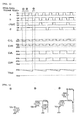
- Fig. 13 is a circuit diagram showing the configuration of a voltage booster circuit 138 in this case.
- the voltage booster circuit 138 is formed of transistors Q1 to Q8, auxiliary capacitors C1, C2, and C2p, and an output capacitor Cout.
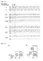
- Fig. 14 is a timing chart of control signals sent to the voltage booster circuit 138.
- a control signal “a” shown in this figure is generated by narrowing the pulse width of a control signal "b,” and is sent to n-channel transistors Q2, Q4, Q6, and Q8 in the voltage booster circuit 138 as gate signals.
- a control signal "b” is supplied to p-channel transistors Q1, Q3, Q5 and Q7 of the voltage-booster circuit 138 as the gate signal.
- transistors Q2, Q4, Q6, and Q8 are turned on whereas the other transistors are turned off in a period indicated by 1 ⁇ in Fig. 14, that is, a period in which only the control signal "a” has an "H” level. Therefore, the auxiliary capacitor C1 is charged with an input voltage Vin since a terminal C1H is connected to the supply line of the input voltage Vin and a terminal C1L is connected to the ground line, as shown in 1 ⁇ of Fig. 15.
- the auxiliary capacitor C2 is connected in parallel to the auxiliary capacitor C2p charged with 2Vin, in a period indicated by 2 ⁇ , and is charged. After these operations, all the transistors Q1 to Q8 are turned off temporarily.
- the auxiliary capacitor C2p since a terminal C2pH of the auxiliary capacitor C2p is connected to the terminal C1H, the auxiliary capacitor C2p is charged with a potential difference of 2Vin. Therefore, the potential of the terminal C2pH becomes 2Vin in the period 2 ⁇ .
- the terminal C1H is connected to a terminal C2L of the auxiliary capacitor C2, which has been charged with 2Vin in the period 2 ⁇ , the potential of the terminal C2H of the auxiliary capacitor C2 becomes 4Vin, which is offset from the potential of the terminal C1H (C2pH, C2L), 2Vin, to a higher potential by the output voltage 2Vin of the auxiliary capacitor C2. And then, the potential is smoothed by the output capacitor Cout. With the periods 1 ⁇ and 2 ⁇ being repeated in this way, the input voltage Vin is boosted four times and outputted.
- auxiliary capacitors C1, C2, C2p, C3, C3p, C4, and C4p are used, as shown in Fig. 16.
- the auxiliary capacitor C1 is charged with an input voltage Vin
- the auxiliary capacitor C2 is connected in parallel to the auxiliary capacitor C2p which has been charged with 2Vin in 2 ⁇ and is charged
- the auxiliary capacitor C3 is connected in parallel to the auxiliary capacitor C3p which has been charged with 4Vin in 2 ⁇ and is charged in the same way
- the auxiliary capacitor C4 is connected in parallel to the auxiliary capacitor C4p which has been charged with 8Vin in 2 ⁇ and is charged in the same way.
- the auxiliary capacitor C2p is first charged with 2Vin, which is offset from the input voltage Vin to a higher potential by the output voltage Vin of the auxiliary capacitor C1; secondly, the auxiliary capacitor C3p is charged with 4Vin, which is offset from a potential of 2Vin caused by the auxiliary capacitor C1 to a higher potential by the output voltage 2Vin of the auxiliary capacitor C2; thirdly, the auxiliary capacitor C4p is charged with 8Vin, which is offset from a potential of 4Vin caused by the auxiliary capacitor C2 to a higher potential by the output voltage 4Vin of the auxiliary capacitor C3; and fourthly, a potential of 16Vin, which is 16 times the input voltage Vin, is obtained by offsetting a potential of 8Vin caused by the auxiliary capacitor C3 to a higher potential by the output voltage 8Vin of the auxiliary capacitor C4.
- the largest problem in the conventional voltage booster circuit is that it is difficult to control the voltage-boost magnification as required. Therefore, to make the boosted voltage constant at the desired voltage value, a separate constant-voltage circuit such as a switching regulator is required at a later stage in the voltage booster circuit, and accordingly, the scale of the power-source circuit becomes large.
- US 5870295 discloses a voltage booster circuit comprising:
- the present invention has been made in consideration of the above situations. Accordingly, it is an object of the present invention to provide a voltage booster circuit and a voltage boosting method which allow the voltage-boost magnification to be controlled relatively freely, and to provide an electronic unit using the output of the voltage booster circuit as a power source.
- a voltage booster circuit comprises: voltage booster circuit comprising:
- the other terminal of the first charge-accumulating device since the first charge-accumulating device is connected between the first and the second lines, the other terminal of the first charge-accumulating device has the same potential as the second line when it is assumed that the first line has a reference potential.
- the one terminal of the first charge-accumulating device is switched from the first line to the second line, since the potential of the other terminal of the first charge-accumulating device is offset from the potential of the second line in the potential direction opposite to that to the first line by the output voltage of the first charge-accumulating device, which is twice the potential of the second line, and the second charge-accumulating device is charged therewith.
- the potential of the output line becomes four times the potential of the second line, which is offset from the potential of the other terminal of the first charge-accumulating device, having a potential that is twice the potential of the second line, in the potential direction opposite to that to the first line by the output voltage of the second charge-accumulating device. Therefore, two charge-accumulating devices are required to boost the potential difference between the first and the second lines four times.
- Such a configuration can be used in a case when the first line has a higher potential than the second line as well as in a case when the first line has a lower potential than the second line.
- the reference potential may be the potential of the first line or that of the second line.
- said voltage boost control circuit is arranged for controlling whether the connection of the second charge-accumulating device is established by said second connection means in the first arrangement or said fourth connection means in the second arrangement.
- the control means controls such that the connection period of the second charge-accumulating device established by the second connection means is set to the entire period and the connection period of the second charge-accumulating device established by the fourth connection means is set to zero, the potential of the output line becomes four times the potential of the second line as described above.
- the control means controls such that the connection period of the second charge-accumulating device established by the second connection means is set to zero and the connection period of the second charge-accumulating device established by the fourth connection means is set to the entire period, since the output voltage of the second charge-accumulating device becomes equal to, not two times, the potential difference between the first line and the second line, the potential of the output line becomes three times the potential of the second line. Therefore, when the potential of the output line is smoothed with the connection-period ratio being controlled, the voltage-boost magnification can be varied to any value between three and four.
- said voltage boost control circuit controls such that the connection period of the second charge-accumulating device established by said second connection means in the first arrangement is longer than the connection period of the second charge-accumulating device established by said fourth connection means in the second arrangement when the potential of the second line or a potential according to the output line is lower in absolute values than a predetermined value.
- the potential of the output line can be made constant between three times and four times the potential of the second line.
- said voltage boost control circuit is arranged for controlling whether the connection of the second charge-accumulating device is established by said second and fourth connection means in the first and second arrangements respectively or the connection is established by said fifth connection means in the third arrangement.
- the control means controls such that the connection period of the second charge-accumulating device established by the second or the fourth connection means is set to the entire period and the connection period of the second charge-accumulating device established by the fifth connection means is set to zero, the potential of the output line becomes four times or three times the potential of the second line as described above.
- the control means controls such that the connection period of the second charge-accumulating device established by the second or the fourth connection means is set to zero and the connection period of the second charge-accumulating device established by the fifth connection means is set to the entire period
- the output line has the same potential as the other terminal of the first charge-accumulating device, having a potential that is two times the potential of the second line. Therefore, when the potential of the output line is smoothed with the connection-period ratio being controlled, the voltage-boost magnification can be varied to any value between four and two, or between three and two.
- said voltage boost control circuit controls such that the connection period of the second charge-accumulating device established by said second and fourth connection means in the first and second arrangements respectively is longer than the connection period established by said fifth connection means in the third arrangement when the potential of the second line or a potential according to the output line is lower in absolute values than a predetermined value.
- the potential of the output line can be made constant between four times and two times, or between three times and two times the potential of the second line.
- said voltage boost control circuit is arranged for controlling whether the connection of the second charge-accumulating device established by said second and fourth connection means in the first and second arrangements respectively or the connection is established by said fifth connection means in the third arrangement, or the connection is established by said sixth connection means in the fourth arrangement.
- the control means controls such that the connection period of the second charge-accumulating device established by the second or the fourth connection means or the connection period established by the fifth connection means is set to the entire period and the connection period established by the sixth connection means is set to zero, the potential of the output line becomes four times, three times, or two times the potential of the second line as described above.
- the control means controls such that the connection period of the second charge-accumulating device established by the second or the fourth connection means or the connection period established by the fifth connection means is set to zero and the connection period of the second charge-accumulating device established by the sixth connection means is set to the entire period, the output line has the same potential as the second line. Therefore, when the potential of the output line is smoothed with the connection-period ratio being controlled, the voltage-boost magnification can be varied to any value between four and one, between three and one, or between two and one.
- said voltage boost control circuit controls such that the connection period of the second charge-accumulating device established by said second and fourth connection means in the first and second arrangements respectively or the connection period established by said fifth connection means in the third arrangement is longer than the connection period established by said sixth connection means in the fourth arrangement when the potential of the second line or a potential according to the output line is lower in absolute values than a predetermined value.
- the potential of the output line can be made constant between four times and the same as the potential of the second line, between three times and the same as the potential of the second line, or between two times and the same as the potential of the second line.
- the voltage booster circuit may comprise n charge accumulating devices whereby the voltage-boost magnification factor can be set to any value between 1 and 2 n . Assuming that "n" is set to four, for example, since the first charge-accumulating device is connected between the first and the second lines, the other terminal of the first charge-accumulating device has the same potential as the second line. Then, when the one terminal of the first charge-accumulating device is switched to the second line, the potential of the other terminal of the first charge-accumulating device is two times the potential of the second line, and the second charge-accumulating device is charged therewith.
- the potential of the other terminal of the second charge-accumulating device becomes four times the potential of the second line, and the third charge-accumulating device is charged therewith.
- the potential of the other terminal of the third charge-accumulating device becomes eight times the potential of the second line, and the fourth charge-accumulating device is charged therewith.
- the potential of the other terminal of the fourth charge-accumulating device becomes 16 times the potential of the second line.
- a voltage boosting method comprising:
- the method may comprise the steps of connecting n charge accumulating devices whereby the voltage-boost magnification factor can be set to any value between 1 and 2 n .
- an electronic unit comprising: a voltage booster circuit as described above, wherein a potential according to the output line is used as a power source.
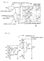
- Fig. 1 is a block diagram showing the configuration of a power-source circuit to which a voltage booster circuit according to the present invention is applied.
- a power-source circuit 100 is formed of a voltage detection circuit 110, a voltage-boost control circuit 120, and a voltage booster circuit 130.
- the voltage detection circuit 110 detects the output voltage Vout of the voltage booster circuit 130 and sends the detection result to the voltage-boost control circuit 120.
- the voltage-boost control circuit 120 generates control signals "a,” "b,” “c1,” “c2,” and "d” used for controlling the voltage-boost magnification of the voltage booster circuit 130 according to the output voltage Vout detected by the voltage detection circuit 110.
- the voltage booster circuit 130 boosts an input voltage Vin between once and four times and outputs the output voltage Vout according to the control signals "a,” “b,” “c1,” “ “c2,” and “d” generated by the voltage-boost control circuit 120.
- the voltage booster circuit 130 is formed of transistors Q2 to Q8 serving as switching devices, auxiliary capacitors C1 (first charge-accumulating device and C2 second charge-accumulating device), and an output capacitor Cout.
- one terminal C1L of the auxiliary capacitor C1 is connected to a ground line (first line) having a reference potential through an n-channel transistor Q4 having the control signal "a" as a gate signal, and is also connected to the supply line (second line) of the input voltage Vin through a p-channel transistor Q3 having the control signal "b" as a gate signal.
- the other terminal C1H of the auxiliary capacitor C1 is connected as described below.
- the terminal C1H is first connected to the supply line of the input voltage Vin through an n-channel transistor Q2 having the control signal "a" as a gate signal; is secondly connected to one terminal C2L of the auxiliary capacitor C2 through a p-channel transistor Q7 having the control signal "d” as a gate signal, and is further connected to the ground line through an n-channel transistor Q8 having the control signal "c2" as a gate signal; and is fourthly connected to the other terminal C2H of the auxiliary capacitor C2 through an n-channel transistor Q6 having the control signal "c1" as a gate signal, and is further connected to the output line of the output voltage Vout through a p-channel transistor Q5 having the control signal "d” as a gate signal.
- the output capacitor Cout is connected in parallel between the output line and the ground line in order to smooth the output voltage Vout.
- the operation of the power-source circuit 100 having the above configuration will be described next.
- the voltage-boost control circuit 120 essentially controls the voltage-boost magnification of the voltage booster circuit 130 in any range according to the output voltage Vout, but for the sake of convenience, the operation of the power-source circuit 100 will be described for each of the cases in which the voltage-boost magnification is set to four, three, two, and one, and then for a case in which the voltage-boost magnification is set to any value.
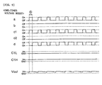
- the voltage-boost control circuit 120 generates control signals "a,” “b,” “c1,” “c2,” and “d” as shown by a timing chart illustrated in Fig. 3.
- the control signal "a” is formed by narrowing the pulse width of the control signal "b.”
- the control signals "c1” and “c2” are formed by inverting the control signal “b” and scaling it down by a factor of 2 (thinning the number of pulse to 1/2).
- the control signal “d” is formed by inverting the control signal "c1” or "c2” and delaying it by half the period.
- the auxiliary capacitor C2 is charged with 2Vin, which is the potential difference between both terminals. After this operation, the transistors Q2 to Q8 are all turned off temporarily.
- the potential of the terminal C2H becomes 4Vin, which is offset from the potential of the terminal C1H (C2L), 2Vin, to a higher potential by the output voltage 2Vin of the auxiliary capacitor C2, and then, it is smoothed by the output capacitor Cout.
- the output voltage Vout is gradually reduced from 4Vin in a period from when the transistor Q5 is turned off to when it is turned on.
- the periods 1 ⁇ , 2 ⁇ , and 3 ⁇ are repeated to boost the input voltage Vin four times and to output it.
- the voltage-boost control circuit 120 generates control signals "a,” “b,” “c1,” “c2,” and “d” shown in a timing chart illustrated in Fig. 5.
- the control signals "a” and “b” are the same as those used in the four-times voltage boost.
- the control signals "c1” and “c2” are the same as the control signal "a,” and, in the same way, the control signal "d” is the same as the control signal "b".
- the transistors Q2, Q4, Q6, and Q8 are turned on whereas the other transistors are all turned off in a period indicated by 1 ⁇ in Fig. 5, namely, in a period when all the control signals "a,” “b,” “c1,” "c2,” and “d” have an "H” level. Therefore, since the auxiliary capacitors C1 and C2 are connected in parallel such that the terminal C1H and the terminal C2H are connected to the supply line of the input voltage Vin and the terminal C1L and the terminal C2L are connected to the ground line, as indicated by 1 ⁇ in Fig. 6, the auxiliary capacitors C1 and C2 are charged with the input voltage Vin. After this operation, the transistors Q2 to Q8 are all turned off temporarily.
- the potential of the terminal C2H becomes 3Vin, which is offset from the potential of the terminal C1H (C2L), 2Vin, to a higher potential by the output voltage Vin of the auxiliary capacitor C2.
- the output voltage Vout is gradually reduced from 3Vin in a period from when the transistor Q5 is turned off to when it is turned on.
- the periods 1 ⁇ and 2 ⁇ are repeated to boost the input voltage Vin three times and to output it.
- the voltage-boost control circuit 120 generates control signals "a,” “b,” “c1,” “c2,” and “d” shown in a timing chart illustrated in Fig. 7.
- the control signals "a” and “b” are the same as those used in the four-times and three-times voltage boosts.
- the control signal “c1” is formed by inverting the control signal "b.”
- the control signal “c2” always has an "L” level.
- the control signal “d” is the same as the control signal "b.”
- the transistors Q2 and Q4 are turned on whereas the other transistors are all turned off in a period indicated by 1 ⁇ in Fig. 7, namely, in a period when the control signals "a,” “b,” and “d” have an "H” level except for the control signal "c1" and "c2", as in the period indicated by 1 ⁇ in the four-times voltage boost. Therefore, as shown in 1 ⁇ in Fig. 8, the auxiliary capacitor C1 is charged with the input voltage Vin. After this operation, the transistors Q2 to Q8 are all turned off temporarily.
- the periods 1 ⁇ and 2 ⁇ are repeated to boost the input voltage Vin twice and to output it.
- the voltage-boost control circuit 120 generates control signals "a,” “b,” “c1,” “c2,” and “d” shown in a timing chart illustrated in Fig. 9.
- the control signal "a” is the same as that used in the four-times, three-times, and two-times voltage boosts.
- the control signal "b” always has an "H” level.
- the control signal "c1” is the same as the control signal "a”.
- the control signal “c2” always has a "L” level.
- the control signal “d” is formed by inverting the control signal "a” or "c1".
- the input voltage Vin is output as is as the output voltage Vout.
- the voltage booster circuit in the present embodiment allows four-times, three-times, two-times, and one-times voltage boosts.
- the magnification is actually allowed to be changed to any value between four and one.
- the voltage-boost control circuit 120 sends control signals for different voltage-boost magnifications in a time-division manner and controls the ratio of the supply periods to allow the voltage-boost magnification to be set to a value between the different magnifications.
- the output voltage Vout which is smoothed by the output capacitor Cout
- the voltage-boost magnification is substantially set to 3.5.
- the control signals for the four-times voltage boost and the control signals for the three-times voltage boost are alternately sent with respective supply-period ratios of 25% and 75%, for example, the voltage-boost magnification is substantially set to 3.25. In either case, since the control signals "a" and "b" are used in common, only the control signal "c1" ("c2") and the control signal "d" need to be changed.
- controlling the supply-period ratio of the control signals means exclusively controlling the connection patterns required to obtain each voltage in a time-division manner.
- a combination of the control signals for the four-times voltage boost and those for the two-times or one-times voltage boost can be used in addition to a combination of the control signals for the four-times voltage boost and those for the three-times voltage boost.
- control signals for the four-times voltage boost and those for the two-times voltage boost need to be alternately sent with the respective supply-period ratios of 75 % and 25%, or the control signals for the four-times voltage boost and those for the one-times voltage boost need to be alternately sent with the respective supply-period ratios of 83.3% and 16.7%.
- a combination of the control signals for the four-times voltage boost and those for the two-times or one-times voltage boost or a combination of the control signals for the three-times voltage boost and those for the one-times voltage boost can be used in addition to a combination of the control signals for the three-times voltage boost and those for the two-times voltage boost.
- a combination of the control signals for the four-times or three-times voltage boost and those for the one-times voltage boost can be used in addition to a combination of the control signals for the two-times voltage boost and those for the once voltage boost.
- Such a control is actually performed in the following way.
- the period when the control signals for a higher-magnification voltage boost are sent is set shorter than the period when the control signals for a lower-magnification voltage boost are sent.
- the period when the control signals for a higher-magnification voltage boost are sent is set longer than the period when the control signals for a lower-magnification voltage boost are sent.
- feedback control is used to make the output voltage Vout constant, in which control signals for each voltage-boost magnification are sent in a time-division manner according to the comparison between the target voltage Vref and the output voltage Vout, and the supply-period ratio is controlled.
- the present invention is not limited to the use of this control.
- the voltage-boost control circuit 120 may be configured such that the output voltage Vout is made constant by feed-forward control in which control signals for each voltage-boost magnification are sent in a time-division manner according to the comparison with the input voltage Vin and the supply-period ratio is controlled.
- FIG. 10 is a circuit diagram showing the configuration of a voltage booster circuit 132 in the present embodiment.
- the voltage booster circuit 132 shown in this figure is used in the power-source circuit 100 instead of the voltage booster circuit 130 shown in Fig. 2.
- the voltage booster circuit 132 is formed by adding auxiliary capacitors C3 and C4 to the voltage booster circuit 130 in the first embodiment. Details will be described next.
- a terminal C2H of an auxiliary circuit C2 is first connected to one terminal C3L of an auxiliary capacitor C3 through a p-channel transistor Q10 having a control signal "f” as a gate signal and is further connected to a ground line through an n-channel transistor Q11 having a control signal "e” as a gate signal; and is secondly connected to the other terminal C3H of the auxiliary capacitor C3 through an n-channel transistor Q9 having the control signal "e” as a gate signal.
- the terminal C3H of the auxiliary capacitor C3 is first connected to one terminal C4L of an auxiliary capacitor C4 through a p-channel transistor Q14 having a control signal "g" as a gate signal and is further connected to the ground line through an n-channel transistor Q15 having a control signal "h2" as a gate signal; and is secondly connected to the other terminal C4H of the auxiliary capacitor C4 through an n-channel transistor Q13 having a control signal "h1" as a gate signal and is further connected to the output line of the output voltage Vout through a p-channel transistor Q12 having the control signal "g” as a gate signal.
- An output capacitor Cout is connected in parallel between the output line and the ground line to smooth the output voltage Vout, in the same way as in the first embodiment.
- the voltage-boost control circuit 120 sends control signals in the following periods 1 ⁇ to 5 ⁇ to control switching of each of the transistors Q2 to Q15 in the voltage booster circuit 132.
- the voltage-boost control circuit 120 first connects the terminal C1H to the supply line of the input voltage Vin and also connects the terminal C1L to the ground line as indicated in 1 ⁇ in Fig. 11. With this operation, the auxiliary capacitor C1 is charged with Vin.
- the voltage-boost control circuit 120 connects the terminal C1L to the supply line of the input voltage Vin, the terminal C1H to the terminal C2H, and then the terminal C2L to the ground line as indicated in 2 ⁇ in the figure. With this operation, the potential of the terminal C1H becomes 2Vin, which is offset from the input voltage Vin to a higher potential by the output voltage Vin of the auxiliary capacitor C1, and the auxiliary capacitor C2 is charged with 2Vin.
- the voltage-boost control circuit 120 connects the terminal C1H to the terminal C2L, the terminal C2H to the terminal C3H, and then the terminal C3L to the ground line while the terminal C1L is connected to the supply line of the input voltage Vin, as indicated in 3 ⁇ in the figure.
- the potential of the terminal C2H becomes 4Vin, which is offset from the potential 2Vin of the terminal C1H (C2L) to a higher potential by the output voltage 2Vin of the auxiliary capacitor C2, and the auxiliary capacitor C3 is charged with 4Vin.
- the voltage-boost control circuit 120 connects the terminal C2H to the terminal C3L, the terminal C3H to the terminal C4H, and then the terminal C4L to the ground line while the terminal C1L is connected to the supply line of the input voltage Vin and the terminal C1H is connected to the terminal C2L, as indicated in 4 ⁇ in the figure.
- the potential of the terminal C3H becomes 8Vin, which is offset from the potential 4Vin of the terminal C2H (C3L) to a higher potential by the output voltage 4Vin of the auxiliary capacitor C3, and the auxiliary capacitor C4 is charged with 8Vin.
- the voltage-boost control circuit 120 connects the terminal C3H to the terminal C4L and the terminal C4H to the output line of the output voltage Vout while the terminal C1L is connected to the supply line of the input voltage Vin, the terminal C1H is connected to the terminal C2L, and the terminal C2H is connected to the terminal C3L, as indicated in 5 ⁇ in the figure.
- the potential of the output line becomes 16Vin, which is offset from the potential 8Vin of the terminal C3H (C4L) to a higher potential by the output voltage 8Vin of the auxiliary capacitor C4. In this way, a 16-times voltage boost is performed with the four auxiliary capacitors C1 to C4.
- the auxiliary capacitors C1 to C4 can be charged with the following potentials in the present embodiment.
- the auxiliary capacitor C1 can be charged with Vin
- the auxiliary capacitor C2 can be charged with Vin or 2Vin
- the auxiliary capacitor C3 is charged with Vin, 2Vin, 3Vin, or 4Vin
- the auxiliary capacitor C4 can be charged with 0, Vin, 2Vin, ..., 7Vin, and 8Vin. Therefore, the supply line of the input voltage Vin is offset by the output voltage obtained by appropriately combining the auxiliary capacitors C1 to C4 to allow an output voltage Vout of Vin, 2Vin, 3Vin, ..., or 16Vin to be obtained.
- the voltage-boost control circuit 120 sends control signals specifying each voltage-boost magnification in a time-division manner and controls the supply-period ratio to allow the voltage-boost magnification to be controlled at any value between 16 and one. Furthermore, the voltage-boost control circuit 120 controls the supply-period ratio according to the result of comparison between the output voltage Vout and the target voltage Vref to allow the output voltage Vout to be made constant between 16Vin and Vin.
- the first and second embodiment are extended, namely, auxiliary capacitors are added in the same way, to allow the input voltage Vin to be boosted 32 times, 64 times, ..., and 2 n times.
- auxiliary capacitors are required for a voltage boost, the configuration can be simplified.
- the voltage-boost magnification can be set to any value between 2 n and one, and further, the output voltage Vout can be made constant therebetween.
- auxiliary capacitors are used for charging and offsetting.
- devices are not limited to auxiliary capacitors. Secondary cells, for example, may be used.
- a positive power source in which the input voltage Vin is set to be in a positive side of the reference potential and the offset direction is set to the positive direction.
- the present invention is not limited to this case.
- the present invention can also be applied to a negative power source in which the input voltage is set to be in the negative side of the reference potential and the offset direction is set to the negative direction.
- connections and switching of the auxiliary capacitors are performed by transistors.
- Other various switches such as analog switches and transmission gates may be used.
- the voltage booster circuit 130 in the first embodiment, the voltage booster circuit 132 in the second embodiment, and a voltage booster circuit obtained by extending these voltage booster circuits can be used, for example, as a power-source circuit that sends electrical power to each section of a liquid-crystal display apparatus.
- Fig. 12 is a block diagram showing the electrical configuration of this liquid-crystal display apparatus.
- a liquid-crystal display panel 200 has a liquid-crystal device 202 formed at each intersection of i data lines X1 to Xi and j scanning lines Y1 to Yj.
- Each liquid-crystal device 202 has a configuration in which a liquid-crystal display element (liquid-crystal layer) 204 and a thin-film diode (hereinafter called a TFD) device 206 are connected in series.
- a liquid-crystal display element liquid-crystal layer
- a TFD thin-film diode
- the scanning lines Y1 to Yj are driven by a scanning-signal driving circuit 210, and the data lines X1 to Xi are driven by a data-signal driving circuit 220.
- the scanning-signal driving circuit 210 and the data-signal driving circuit 220 are controlled by a driving control circuit 240.
- the TFD device 206 is connected to a scanning line and the liquid-crystal layer 204 is connected to a data line.
- the configuration may be formed such that the TFD device 206 is connected to a data line and the liquid-crystal layer 204 is connected to a scanning line.
- a power-source circuit 100 controls the voltage-boost magnification of an input voltage Vin to output various output voltages, such as various selection voltages used in the scanning-signal driving circuit 210, data-signal voltages used in the data-signal driving circuit 220, and voltages used in the driving control circuit 240.
- the voltage booster circuit 130 described above, is applied to the power-source circuit 100.
- liquid-crystal display apparatus various types can be employed such as an active-matrix type using thin-film transistors (TFT) and a passive-matrix type not using switching elements such as TFDs and TFTs.
- TFT thin-film transistors
- the voltage booster circuit according to the present invention can also be applied to a power-source circuit of an electroluminescence (EL) display apparatus, in addition to that of the liquid-crystal apparatus, in which row electrodes and column electrodes are formed on an insulating layer covering an EL layer.
- EL electroluminescence
- an electronic unit according to the present invention can be applied not only to display apparatuses but also to projectors, personal computers, pagers, liquid-crystal TV sets, viewfinder-type and monitor-view-type video cassette recorders, car-navigation apparatuses, electronic notebooks, electric calculators, wordprocessors, workstations, cellular phones, videophones, POS terminals, and apparatuses having touch-sensitive panels.
Landscapes
- Engineering & Computer Science (AREA)
- Power Engineering (AREA)
- Dc-Dc Converters (AREA)
- Control Of Indicators Other Than Cathode Ray Tubes (AREA)
- Direct Current Feeding And Distribution (AREA)
- Charge And Discharge Circuits For Batteries Or The Like (AREA)
Description
- The present invention relates to voltage booster circuits and voltage boosting methods which reduce the number of charge-accumulating devices required for a voltage boost and electronic units using the output of such a voltage booster circuit as a power source.
- In liquid-crystal display apparatuses, for example, a high-voltage power source is required to drive liquid-crystal devices in order to obtain successful display characteristics. Therefore, a power-source circuit used in the liquid-crystal display apparatuses is configured such that an input voltage is boosted by a voltage booster circuit and the boosted voltage is supplied to a driving circuit for driving the liquid-crystal devices and to other circuits.
- The configuration of a conventional voltage booster circuit will be described below for a case in which a voltage-boost magnification set to four is taken as an example. Fig. 13 is a circuit diagram showing the configuration of a
voltage booster circuit 138 in this case. Thevoltage booster circuit 138 is formed of transistors Q1 to Q8, auxiliary capacitors C1, C2, and C2p, and an output capacitor Cout. - Fig. 14 is a timing chart of control signals sent to the
voltage booster circuit 138. A control signal "a" shown in this figure is generated by narrowing the pulse width of a control signal "b," and is sent to n-channel transistors Q2, Q4, Q6, and Q8 in thevoltage booster circuit 138 as gate signals. A control signal "b" is supplied to p-channel transistors Q1, Q3, Q5 and Q7 of the voltage-booster circuit 138 as the gate signal. - When the control signals "a" and "b" are sent to the
voltage booster circuit 138, transistors Q2, Q4, Q6, and Q8 are turned on whereas the other transistors are turned off in a period indicated by 1 ○ in Fig. 14, that is, a period in which only the control signal "a" has an "H" level. Therefore, the auxiliary capacitor C1 is charged with an input voltage Vin since a terminal C1H is connected to the supply line of the input voltage Vin and a terminal C1L is connected to the ground line, as shown in 1 ○ of Fig. 15. The auxiliary capacitor C2 is connected in parallel to the auxiliary capacitor C2p charged with 2Vin, in a period indicated by 2 ○, and is charged. After these operations, all the transistors Q1 to Q8 are turned off temporarily. - In a period indicated by 2 ○ in Fig. 14, that is, a period in which both control signals "a" and "b" have an "L" level, transistors Q1, Q3, Q5, and Q7 are turned on whereas the other transistors are turned off. Therefore, as shown in 2 ○ of Fig. 14, since the terminal C1L of the auxiliary capacitor C1 is switched and connected to the supply line of the input voltage Vin and the terminal C1H is disconnected from the supply line of the input voltage Vin, the potential of the terminal C1H becomes 2Vin, which is offset from the input voltage Vin to a higher potential by the output voltage Vin of the auxiliary capacitor C1. On the other hand, since a terminal C2pH of the auxiliary capacitor C2p is connected to the terminal C1H, the auxiliary capacitor C2p is charged with a potential difference of 2Vin. Therefore, the potential of the terminal C2pH becomes 2Vin in the period 2 ○. In addition, since the terminal C1H is connected to a terminal C2L of the auxiliary capacitor C2, which has been charged with 2Vin in the period 2 ○, the potential of the terminal C2H of the auxiliary capacitor C2 becomes 4Vin, which is offset from the potential of the terminal C1H (C2pH, C2L), 2Vin, to a higher potential by the output voltage 2Vin of the auxiliary capacitor C2. And then, the potential is smoothed by the output capacitor Cout. With the
periods 1 ○ and 2 ○ being repeated in this way, the input voltage Vin is boosted four times and outputted. - To increase the voltage-boost magnification, for example, to set the voltage-boost magnification to 16, seven auxiliary capacitors C1, C2, C2p, C3, C3p, C4, and C4p are used, as shown in Fig. 16. As shown in 1 ○ of the figure, the auxiliary capacitor C1 is charged with an input voltage Vin, the auxiliary capacitor C2 is connected in parallel to the auxiliary capacitor C2p which has been charged with 2Vin in 2 ○ and is charged, the auxiliary capacitor C3 is connected in parallel to the auxiliary capacitor C3p which has been charged with 4Vin in 2 ○ and is charged in the same way, and the auxiliary capacitor C4 is connected in parallel to the auxiliary capacitor C4p which has been charged with 8Vin in 2 ○ and is charged in the same way.
- As shown in 2 ○ of the figure, the auxiliary capacitor C2p is first charged with 2Vin, which is offset from the input voltage Vin to a higher potential by the output voltage Vin of the auxiliary capacitor C1; secondly, the auxiliary capacitor C3p is charged with 4Vin, which is offset from a potential of 2Vin caused by the auxiliary capacitor C1 to a higher potential by the output voltage 2Vin of the auxiliary capacitor C2; thirdly, the auxiliary capacitor C4p is charged with 8Vin, which is offset from a potential of 4Vin caused by the auxiliary capacitor C2 to a higher potential by the output voltage 4Vin of the auxiliary capacitor C3; and fourthly, a potential of 16Vin, which is 16 times the input voltage Vin, is obtained by offsetting a potential of 8Vin caused by the auxiliary capacitor C3 to a higher potential by the output voltage 8Vin of the auxiliary capacitor C4.
- In the conventional voltage booster circuit, however, if the smoothing capacitor Cout is excluded, three capacitors are required for a four-times voltage boost and seven capacitors are required for a 16-times voltage boost. Generally, (2n - 1) capacitors are required for a 2n-times voltage boost. When a power-source circuit including a voltage booster circuit is integrated, it is difficult to form capacitive circuits such as capacitors on a semiconductor substrate. Even if such a capacitive circuit can be formed, since it makes the circuit size larger, the number of capacitors required for a voltage boost needs to be reduced as much as possible.
- The largest problem in the conventional voltage booster circuit is that it is difficult to control the voltage-boost magnification as required. Therefore, to make the boosted voltage constant at the desired voltage value, a separate constant-voltage circuit such as a switching regulator is required at a later stage in the voltage booster circuit, and accordingly, the scale of the power-source circuit becomes large.
- US 5870295 discloses a voltage booster circuit comprising:
- first connection means for connecting one terminal of a first charge-accumulating device to a first line having a predetermined potential and for connecting the other terminal of the first charge-accumulating device to a second line having a potential different from that of the first line;
- second connection means for connecting one terminal of a second charge-accumulating device to the first line, and for switching and connecting the one terminal of the first charge-accumulating device to the second line and for switching and connecting the other terminal of the first charge-accumulating device to the other terminal of the second charge-accumulating device; and
- third connection means for switching and connecting the one terminal of the second charge-accumulating device to the other terminal of the first charge-accumulating device, for switching and connecting the other terminal of the second charge-accumulating device to an output line and for switching and connecting the one terminal of of the first charge-accumulating device to the second line, said first to third connection means being controllable by a voltage-boost control circuit in a first arrangement to boost a voltage between said first and second lines by a boost magnification factor of 4, the voltage booster circuit further comprising:
- fourth connection means for connecting the one terminal of the second charge-accumulating device to the first line and for connecting the other terminal of the second charge-accumulating device to the second line,
-
- The present invention has been made in consideration of the above situations.
Accordingly, it is an object of the present invention to provide a voltage booster circuit and a voltage boosting method which allow the voltage-boost magnification to be controlled relatively freely, and to provide an electronic unit using the output of the voltage booster circuit as a power source. - To achieve the foregoing object, a voltage booster circuit according to the present invention comprises: voltage booster circuit comprising:
- first connection means for connecting one terminal of a first charge-accumulating device to a first line having a predetermined potential and for connecting the other terminal of the first charge-accumulating device to a second line having a potential different from that of the first line;
- second connection means for connecting one terminal of a second charge-accumulating device to the first line, and for switching and connecting the one terminal of the first charge-accumulating device to the second line and for switching and connecting the other terminal of the first charge-accumulating device to the other terminal of the second charge-accumulating device; and
- third connection means for switching and connecting the one terminal of the second charge-accumulating device to the other terminal of the first charge-accumulating device, for switching and connecting the other terminal of the second charge-accumulating device to an output line and for switching and connecting the one terminal of the first charge-accumulating device to the second line, said first to third connection means being controllable by a voltage-boost control circuit in a first arrangement to boost a voltage between said first and second lines by a boost magnification factor of 4, the voltage booster circuit further comprising at least one of:
- fourth connection means for connecting the one terminal of the second charge-accumulating device to the first line and for connecting the other terminal of the second charge-accumulating device to the second line,
- fifth connection means for connecting the other terminal of the first charge-accumulating device to the output line while the one terminal of the first charge-accumulating device is being connected to the second line,
- sixth connection means for connecting the second line to the output line,
said sixth connection means being controllable by the voltage-boost control circuit in a fourth arrangement to boost a voltage between said first and second lines by a boost magnification factor of 1, and by further comprising: - the voltage-boost control circuit is further arranged to send control signals for different boost magnification factors according to one of said first to fourth arrangements in a time-division manner whereby a ratio of supply periods is controlled so that the voltage boost magnification factor can be set at a value between two different magnifications.
-
- According to the present invention, since the first charge-accumulating device is connected between the first and the second lines, the other terminal of the first charge-accumulating device has the same potential as the second line when it is assumed that the first line has a reference potential. When the one terminal of the first charge-accumulating device is switched from the first line to the second line, since the potential of the other terminal of the first charge-accumulating device is offset from the potential of the second line in the potential direction opposite to that to the first line by the output voltage of the first charge-accumulating device, which is twice the potential of the second line, and the second charge-accumulating device is charged therewith. When the one terminal of the second charge-accumulating device is switched from the first line to the other terminal of the first charge-accumulating device, and the other terminal of the second charge-accumulating device is switched from the other terminal of the first charge-accumulating device to the output line and connected, the potential of the output line becomes four times the potential of the second line, which is offset from the potential of the other terminal of the first charge-accumulating device, having a potential that is twice the potential of the second line, in the potential direction opposite to that to the first line by the output voltage of the second charge-accumulating device. Therefore, two charge-accumulating devices are required to boost the potential difference between the first and the second lines four times. Such a configuration can be used in a case when the first line has a higher potential than the second line as well as in a case when the first line has a lower potential than the second line. The reference potential may be the potential of the first line or that of the second line.
- When the voltage booster circuit comprises said fourth connection means, said voltage boost control circuit is arranged for controlling whether the connection of the second charge-accumulating device is established by said second connection means in the first arrangement or said fourth connection means in the second arrangement.
- With this configuration, if the control means controls such that the connection period of the second charge-accumulating device established by the second connection means is set to the entire period and the connection period of the second charge-accumulating device established by the fourth connection means is set to zero, the potential of the output line becomes four times the potential of the second line as described above. On the other hand, if the control means controls such that the connection period of the second charge-accumulating device established by the second connection means is set to zero and the connection period of the second charge-accumulating device established by the fourth connection means is set to the entire period, since the output voltage of the second charge-accumulating device becomes equal to, not two times, the potential difference between the first line and the second line, the potential of the output line becomes three times the potential of the second line. Therefore, when the potential of the output line is smoothed with the connection-period ratio being controlled, the voltage-boost magnification can be varied to any value between three and four.
- In this case, it is preferred that said voltage boost control circuit controls such that the connection period of the second charge-accumulating device established by said second connection means in the first arrangement is longer than the connection period of the second charge-accumulating device established by said fourth connection means in the second arrangement when the potential of the second line or a potential according to the output line is lower in absolute values than a predetermined value.
- With this control, the potential of the output line can be made constant between three times and four times the potential of the second line.
- When the voltage booster circuit comprises said fifth connection means, said voltage boost control circuit is arranged for controlling whether the connection of the second charge-accumulating device is established by said second and fourth connection means in the first and second arrangements respectively or the connection is established by said fifth connection means in the third arrangement.
- With this configuration, if the control means controls such that the connection period of the second charge-accumulating device established by the second or the fourth connection means is set to the entire period and the connection period of the second charge-accumulating device established by the fifth connection means is set to zero, the potential of the output line becomes four times or three times the potential of the second line as described above. On the other hand, if the control means controls such that the connection period of the second charge-accumulating device established by the second or the fourth connection means is set to zero and the connection period of the second charge-accumulating device established by the fifth connection means is set to the entire period, the output line has the same potential as the other terminal of the first charge-accumulating device, having a potential that is two times the potential of the second line. Therefore, when the potential of the output line is smoothed with the connection-period ratio being controlled, the voltage-boost magnification can be varied to any value between four and two, or between three and two.
- In this case, it is preferred that said voltage boost control circuit controls such that the connection period of the second charge-accumulating device established by said second and fourth connection means in the first and second arrangements respectively is longer than the connection period established by said fifth connection means in the third arrangement when the potential of the second line or a potential according to the output line is lower in absolute values than a predetermined value. With this control, the potential of the output line can be made constant between four times and two times, or between three times and two times the potential of the second line.
- When the voltage booster circuit comprises said sixth connection means said voltage boost control circuit is arranged for controlling whether the connection of the second charge-accumulating device established by said second and fourth connection means in the first and second arrangements respectively or the connection is established by said fifth connection means in the third arrangement, or the connection is established by said sixth connection means in the fourth arrangement.
- With this configuration, if the control means controls such that the connection period of the second charge-accumulating device established by the second or the fourth connection means or the connection period established by the fifth connection means is set to the entire period and the connection period established by the sixth connection means is set to zero, the potential of the output line becomes four times, three times, or two times the potential of the second line as described above. On the other hand, if the control means controls such that the connection period of the second charge-accumulating device established by the second or the fourth connection means or the connection period established by the fifth connection means is set to zero and the connection period of the second charge-accumulating device established by the sixth connection means is set to the entire period, the output line has the same potential as the second line. Therefore, when the potential of the output line is smoothed with the connection-period ratio being controlled, the voltage-boost magnification can be varied to any value between four and one, between three and one, or between two and one.
- In this case, it is preferred that said voltage boost control circuit controls such that the connection period of the second charge-accumulating device established by said second and fourth connection means in the first and second arrangements respectively or the connection period established by said fifth connection means in the third arrangement is longer than the connection period established by said sixth connection means in the fourth arrangement when the potential of the second line or a potential according to the output line is lower in absolute values than a predetermined value. With this control, the potential of the output line can be made constant between four times and the same as the potential of the second line, between three times and the same as the potential of the second line, or between two times and the same as the potential of the second line.
- The voltage booster circuit may comprise n charge accumulating devices whereby the voltage-boost magnification factor can be set to any value between 1 and 2n. Assuming that "n" is set to four, for example, since the first charge-accumulating device is connected between the first and the second lines, the other terminal of the first charge-accumulating device has the same potential as the second line. Then, when the one terminal of the first charge-accumulating device is switched to the second line, the potential of the other terminal of the first charge-accumulating device is two times the potential of the second line, and the second charge-accumulating device is charged therewith. Then, when the one terminal of the second charge-accumulating device is switched to the other terminal of the first charge-accumulating device, the potential of the other terminal of the second charge-accumulating device becomes four times the potential of the second line, and the third charge-accumulating device is charged therewith. Then, when the one terminal of the third charge-accumulating device is switched to the other terminal of the second charge-accumulating device, the potential of the other terminal of the third charge-accumulating device becomes eight times the potential of the second line, and the fourth charge-accumulating device is charged therewith. Then, when the one terminal of the fourth charge-accumulating device is switched to the other terminal of the third charge-accumulating device, the potential of the other terminal of the fourth charge-accumulating device becomes 16 times the potential of the second line. Therefore, when "n" is set to four, four charge-accumulating devices are required to boost the potential difference between the first and the second lines 24 = 16 times, and thus the configuration is simplified. In other words, when "n" is set to an integer of three or more, n charge-accumulating devices are required to boost the potential difference between the first and the second lines 2n times, and especially when "n" is set to a large integer, the present invention is convenient to simplify the configuration.
- According to another aspect of the present invention, there is provided a voltage boosting method comprising:
- a first step of connecting one terminal of a first charge-accumulating device to a first line having a predetermined potential and of connecting the other terminal of the first charge-accumulating device to a second line having a potential different from that of the first line;
- a second step of connecting one terminal of a second charge-accumulating device to the first line, and of switching and connecting the one terminal of the first charge-accumulating device to the second line and of switching and connecting the other terminal of the first charge-accumulating device to the other terminal of the second charge-accumulating device; and
- a third step of switching and connecting the one terminal of the second charge-accumulating device to the other terminal of the first charge-accumulating device and of switching and connecting the other terminal of the second charge-accumulating device to an output line, said first to third steps being controllable in a first arrangement to boost a voltage between said first and second lines by a boost magnification factor of 4, the method characterised by further comprising at least one of:
- a fourth step of connecting the one terminal of the second charge-accumulating device to the first line and for connecting the other terminal of the second charge-accumulating device to the second line,
- a fifth step of connecting the other terminal of the first charge-accumulating device to the output line while the one terminal of the first charge-accumulating device is being connected to the second line,
- said first and said fifth steps being controllable in a third arrangement to boost a voltage between said first and second lines by a boost magnification factor of 2; and
- a sixth step of connecting the second line (Vin) to the output line,
-
- The method may comprise the steps of connecting n charge accumulating devices whereby the voltage-boost magnification factor can be set to any value between 1 and 2n.
- According to another aspect of the present invention, there is provided an electronic unit comprising: a voltage booster circuit as described above, wherein a potential according to the output line is used as a power source.
- Embodiments of the present invention will now be described by way of further example only and with reference to the accompanying drawings, in which:-
- Fig. 1 is a block diagram showing a power-source circuit to which a voltage booster circuit according to a first embodiment of the present invention is applied.
- Fig. 2 is a circuit diagram showing the configuration of the voltage booster circuit.
- Fig. 3 is a timing chart showing control signals for a four-times voltage boost in the voltage booster circuit.
- Fig. 4 is an operational view for the four-times voltage boost in the voltage booster circuit.
- Fig. 5 is a timing chart showing control signals for a three-times voltage boost in the voltage booster circuit.
- Fig. 6 is an operational view for the three-times voltage boost in the voltage booster circuit.
- Fig. 7 is a timing chart showing control signals for a two-times voltage boost in the voltage booster circuit.
- Fig. 8 is an operational view for the two-times voltage boost in the voltage booster circuit.
- Fig. 9 is a timing chart showing control signals for a one-times voltage boost in the voltage booster circuit.
- Fig. 10 is a circuit diagram showing the configuration of a voltage booster circuit according to a second embodiment of the present invention.
- Fig. 11 is an operational view for a 16-times voltage boost in the voltage booster circuit.
- Fig. 12 is a block diagram showing the electrical configuration of a liquid-crystal display apparatus to which a voltage booster circuit according to an embodiment is applied as a power-source circuit.
- Fig. 13 is a circuit diagram showing the configuration of a conventional voltage booster circuit.
- Fig. 14 is a timing chart showing control signals for a four-times voltage boost in the conventional voltage booster circuit.
- Fig. 15 is an operational view for the four-times voltage boost in the conventional voltage booster circuit.
- Fig. 16 is an operational view for a 16-times voltage boost in the conventional voltage booster circuit.
-
- A first embodiment, which shows a fundamental configuration of the present invention, will be described first. Fig. 1 is a block diagram showing the configuration of a power-source circuit to which a voltage booster circuit according to the present invention is applied. As shown in this figure, a power-
source circuit 100 is formed of avoltage detection circuit 110, a voltage-boost control circuit 120, and avoltage booster circuit 130. Among these, thevoltage detection circuit 110, for example, detects the output voltage Vout of thevoltage booster circuit 130 and sends the detection result to the voltage-boost control circuit 120. The voltage-boost control circuit 120 generates control signals "a," "b," "c1," "c2," and "d" used for controlling the voltage-boost magnification of thevoltage booster circuit 130 according to the output voltage Vout detected by thevoltage detection circuit 110. - A detailed configuration of the
voltage booster circuit 130 will be described below by referring to Fig. 2. Thevoltage booster circuit 130 boosts an input voltage Vin between once and four times and outputs the output voltage Vout according to the control signals "a," "b," "c1," " "c2," and "d" generated by the voltage-boost control circuit 120. Thevoltage booster circuit 130 is formed of transistors Q2 to Q8 serving as switching devices, auxiliary capacitors C1 (first charge-accumulating device and C2 second charge-accumulating device), and an output capacitor Cout. - To describe the configuration in detail, one terminal C1L of the auxiliary capacitor C1 is connected to a ground line (first line) having a reference potential through an n-channel transistor Q4 having the control signal "a" as a gate signal, and is also connected to the supply line (second line) of the input voltage Vin through a p-channel transistor Q3 having the control signal "b" as a gate signal.
- On the other hand, the other terminal C1H of the auxiliary capacitor C1 is connected as described below. The terminal C1H is first connected to the supply line of the input voltage Vin through an n-channel transistor Q2 having the control signal "a" as a gate signal; is secondly connected to one terminal C2L of the auxiliary capacitor C2 through a p-channel transistor Q7 having the control signal "d" as a gate signal, and is further connected to the ground line through an n-channel transistor Q8 having the control signal "c2" as a gate signal; and is fourthly connected to the other terminal C2H of the auxiliary capacitor C2 through an n-channel transistor Q6 having the control signal "c1" as a gate signal, and is further connected to the output line of the output voltage Vout through a p-channel transistor Q5 having the control signal "d" as a gate signal.
- The output capacitor Cout is connected in parallel between the output line and the ground line in order to smooth the output voltage Vout.
- The operation of the power-
source circuit 100 having the above configuration will be described next. The voltage-boost control circuit 120 essentially controls the voltage-boost magnification of thevoltage booster circuit 130 in any range according to the output voltage Vout, but for the sake of convenience, the operation of the power-source circuit 100 will be described for each of the cases in which the voltage-boost magnification is set to four, three, two, and one, and then for a case in which the voltage-boost magnification is set to any value. - The operation will be described first for a case in which the voltage-boost magnification of the voltage-
boost circuit 130 is set to four. In this case, the voltage-boost control circuit 120 generates control signals "a," "b," "c1," "c2," and "d" as shown by a timing chart illustrated in Fig. 3. As shown in the figure, the control signal "a" is formed by narrowing the pulse width of the control signal "b." The control signals "c1" and "c2" are formed by inverting the control signal "b" and scaling it down by a factor of 2 (thinning the number of pulse to 1/2). The control signal "d" is formed by inverting the control signal "c1" or "c2" and delaying it by half the period. - When these control signals are sent to the
voltage booster circuit 130, the transistors Q2 and Q4 are turned on whereas the other transistors are all turned off in a period indicated by 1 ○ in Fig. 3, namely, in a period when the control signals "a," "b," and "d" have an "H" level and the control signals "c1" and "c2" have an "L" level. Therefore, since the terminal C1H of the auxiliary capacitor C1 is connected to the supply line of the input voltage Vin and the terminal C1L is connected to the ground line, as indicated by 1 ○ in Fig. 4, the auxiliary capacitor C1 is charged with the input voltage Vin. After this operation, the transistors Q2 to Q8 are all turned off temporarily. - In a period indicated by 2 ○ in Fig. 3, namely, in a period when the control signals "c1," "c2," and "d" have an "H" level and the control signals "a" and "b" have an "L" level, the transistors Q3, Q6, and Q8 are turned on whereas the other transistors are all turned off. Therefore, since the terminal C1L of the auxiliary capacitor C1 is connected to the supply line of the input voltage Vin and the terminal C1H is disconnected from the supply line of the input voltage Vin, as indicated by 2 ○ in Fig. 4, the potential of the terminal C1H becomes 2Vin, which is offset from the input voltage Vin to a higher potential by the output voltage Vin of the auxiliary capacitor C1. On the other hand, since the terminal C2H of the auxiliary capacitor C2 is connected to the terminal C1H and the terminal C2L is connected to the ground line, the auxiliary capacitor C2 is charged with 2Vin, which is the potential difference between both terminals. After this operation, the transistors Q2 to Q8 are all turned off temporarily.
- In a period indicated by 3 ○ in Fig. 3, namely, in a period when all the control signals "a," "b," "c1," "c2," and "d" have an "L" level, the transistors Q3, Q5, and Q7 are turned on whereas the other transistors are all turned off. Therefore, while the terminal C1L of the auxiliary capacitor C1 is connected to the supply line of the input voltage Vin, the terminal C1H is connected to the terminal C2L and the terminal C2H is connected to the output line of the output voltage Vout, as indicated by 3 ○ in Fig. 4. Consequently, the potential of the terminal C2H becomes 4Vin, which is offset from the potential of the terminal C1H (C2L), 2Vin, to a higher potential by the output voltage 2Vin of the auxiliary capacitor C2, and then, it is smoothed by the output capacitor Cout. When a load is connected to the output line, since the output capacitor Cout is discharged continuously, the output voltage Vout is gradually reduced from 4Vin in a period from when the transistor Q5 is turned off to when it is turned on.
- As described above, the
periods 1 ○, 2 ○, and 3 ○ are repeated to boost the input voltage Vin four times and to output it. - The operation of the power-
source circuit 100 will be described next for a case in which the voltage-boost magnification of the voltage-boost circuit 130 is set to three. In this case, the voltage-boost control circuit 120 generates control signals "a," "b," "c1," "c2," and "d" shown in a timing chart illustrated in Fig. 5. As shown in the figure, the control signals "a" and "b" are the same as those used in the four-times voltage boost. The control signals "c1" and "c2" are the same as the control signal "a," and, in the same way, the control signal "d" is the same as the control signal "b". - When these control signals are sent to the
voltage booster circuit 130, the transistors Q2, Q4, Q6, and Q8 are turned on whereas the other transistors are all turned off in a period indicated by 1 ○ in Fig. 5, namely, in a period when all the control signals "a," "b," "c1," "c2," and "d" have an "H" level. Therefore, since the auxiliary capacitors C1 and C2 are connected in parallel such that the terminal C1H and the terminal C2H are connected to the supply line of the input voltage Vin and the terminal C1L and the terminal C2L are connected to the ground line, as indicated by 1 ○ in Fig. 6, the auxiliary capacitors C1 and C2 are charged with the input voltage Vin. After this operation, the transistors Q2 to Q8 are all turned off temporarily. - In a period indicated by 2 ○ in Fig. 5, namely, in a period when all the control signals "a," "b," "c1," "c2," and "d" have an "L" level, the transistors Q3, Q5, and Q7 are turned on whereas the other transistors are all turned off. Therefore, since the terminal C1L of the auxiliary capacitor C1 is connected to the supply line of the input voltage Vin, as indicated by 2 ○ in Fig. 6, the potential of the terminal C1H becomes 2Vin, which is offset from the input voltage Vin to a higher potential by the output voltage Vin of the auxiliary capacitor C1. In addition, in this condition, since the terminal C1H is connected to the terminal C2L of the auxiliary capacitor C2 and the terminal C2H is connected to the output line of the output voltage Vout, the potential of the terminal C2H becomes 3Vin, which is offset from the potential of the terminal C1H (C2L), 2Vin, to a higher potential by the output voltage Vin of the auxiliary capacitor C2. When a load is being connected to the output line, since the output capacitor Cout is discharged continuously, the output voltage Vout is gradually reduced from 3Vin in a period from when the transistor Q5 is turned off to when it is turned on.
- As described above, the
periods 1 ○ and 2 ○ are repeated to boost the input voltage Vin three times and to output it. - The operation of the power-
source circuit 100 will be described next for a case in which the voltage-boost magnification of the voltage-boost circuit 130 is set to two. In this case, the voltage-boost control circuit 120 generates control signals "a," "b," "c1," "c2," and "d" shown in a timing chart illustrated in Fig. 7. As shown in the figure, the control signals "a" and "b" are the same as those used in the four-times and three-times voltage boosts. The control signal "c1" is formed by inverting the control signal "b." The control signal "c2" always has an "L" level. The control signal "d" is the same as the control signal "b." - When these control signals are sent to the
voltage booster circuit 130, the transistors Q2 and Q4 are turned on whereas the other transistors are all turned off in a period indicated by 1 ○ in Fig. 7, namely, in a period when the control signals "a," "b," and "d" have an "H" level except for the control signal "c1" and "c2", as in the period indicated by 1 ○ in the four-times voltage boost. Therefore, as shown in 1 ○ in Fig. 8, the auxiliary capacitor C1 is charged with the input voltage Vin. After this operation, the transistors Q2 to Q8 are all turned off temporarily. - In a period indicated by 2 ○ in Fig. 7, namely, in a period when the control signals "c1" has an "H" level and the control signals "a," "b," "c2," and "d" have an "L" level, the transistors Q3, Q5, Q6, and Q7 are turned on whereas the other transistors are all turned off. Therefore, as shown in 2 ○ in Fig. 8, since the terminal C1L of the auxiliary capacitor C1 is connected to the supply line of the input voltage Vin and the terminal C1H is connected to the output line of the output voltage Vout, the output voltage Vout becomes 2Vin, which is offset from the input voltage Vin to a higher potential by the output voltage Vin of the auxiliary capacitor C1.
- In this period, since the terminal C2L and the terminal C2H are short-circuited, the auxiliary capacitor C2 is not charged. When a load is connected to the output line, since the output capacitor Cout is discharged continuously, the output voltage Vout is gradually reduced from 2Vin in a period from when the transistor Q5 is turned off to when it is turned on.
- As described above, the
periods 1 ○ and 2 ○ are repeated to boost the input voltage Vin twice and to output it. - The operation of the power-
source circuit 100 will be described next for a case in which the voltage-boost magnification of the voltage-boost circuit 130 is set to one. In this case, the voltage-boost control circuit 120 generates control signals "a," "b," "c1," "c2," and "d" shown in a timing chart illustrated in Fig. 9. As shown in the figure, the control signal "a" is the same as that used in the four-times, three-times, and two-times voltage boosts. The control signal "b" always has an "H" level. The control signal "c1" is the same as the control signal "a". The control signal "c2" always has a "L" level. The control signal "d" is formed by inverting the control signal "a" or "c1". - When these control signals are sent to the
voltage booster circuit 130, the transistors Q2, Q4, Q5, Q6, and Q7 are turned on whereas the other transistors are all turned off in a period indicated by 1 ○ in Fig. 9, namely, in a period when the control signals "a" and "b" have an "H" level and the control signal "d" has an "L" level. Therefore, since the supply line of the input voltage Vin is connected to the output line, the input voltage Vin is output as is as the output voltage Vout. In this period, since the terminal C2L and the terminal C2H are short-circuited, the auxiliary capacitor C2 is not charged. When a load is being connected to the output line, since the output capacitor Cout is discharged continuously, the output voltage Vout is gradually reduced from Vin in a period from when the transistor Q5 is turned off to when it is turned on. - As described above, with the
period 1 ○, the input voltage Vin is output as is as the output voltage Vout. - As described above, the voltage booster circuit in the present embodiment allows four-times, three-times, two-times, and one-times voltage boosts. In addition to these voltage-boost magnifications, the magnification is actually allowed to be changed to any value between four and one. In other words, the voltage-
boost control circuit 120 sends control signals for different voltage-boost magnifications in a time-division manner and controls the ratio of the supply periods to allow the voltage-boost magnification to be set to a value between the different magnifications. - When the control signals for the four-times voltage boost and the control signals for the three-times voltage boost are alternately sent for the same period of time, for example, the output voltage Vout, which is smoothed by the output capacitor Cout, is set to 3.5-times the input voltage Vin, which means the voltage-boost magnification is substantially set to 3.5. When the control signals for the four-times voltage boost and the control signals for the three-times voltage boost are alternately sent with respective supply-period ratios of 25% and 75%, for example, the voltage-boost magnification is substantially set to 3.25. In either case, since the control signals "a" and "b" are used in common, only the control signal "c1" ("c2") and the control signal "d" need to be changed.
- In the present embodiment, as described above, since the connections of the auxiliary capacitors C1 and C2 are controlled in a time-division manner to obtain each of voltages 4Vin, 3Vin, 2Vin, and Vin, controlling the supply-period ratio of the control signals means exclusively controlling the connection patterns required to obtain each voltage in a time-division manner.
- To set the voltage-boost magnification between four and three, a combination of the control signals for the four-times voltage boost and those for the two-times or one-times voltage boost can be used in addition to a combination of the control signals for the four-times voltage boost and those for the three-times voltage boost. To describe this with a voltage-boost magnification of 3.5, described above, taken as an example, the control signals for the four-times voltage boost and those for the two-times voltage boost need to be alternately sent with the respective supply-period ratios of 75 % and 25%, or the control signals for the four-times voltage boost and those for the one-times voltage boost need to be alternately sent with the respective supply-period ratios of 83.3% and 16.7%.
- To set the voltage-boost magnification between three and two, a combination of the control signals for the four-times voltage boost and those for the two-times or one-times voltage boost or a combination of the control signals for the three-times voltage boost and those for the one-times voltage boost can be used in addition to a combination of the control signals for the three-times voltage boost and those for the two-times voltage boost. In the same way, to set the voltage-boost magnification between two and one, a combination of the control signals for the four-times or three-times voltage boost and those for the one-times voltage boost can be used in addition to a combination of the control signals for the two-times voltage boost and those for the once voltage boost. When control signals for voltage boosts having a large voltage-boost difference are combined, since the output capacitor Cout smooths voltages having a large potential difference, it is noted that the ripple of the output voltage becomes large.
- Such a control is actually performed in the following way. When the output voltage Vout is higher in absolute values than the target voltage Vref, the period when the control signals for a higher-magnification voltage boost are sent is set shorter than the period when the control signals for a lower-magnification voltage boost are sent. Conversely, when the output voltage Vout is lower in absolute values than the target voltage Vref, the period when the control signals for a higher-magnification voltage boost are sent is set longer than the period when the control signals for a lower-magnification voltage boost are sent. With this control, the output voltage Vout is balanced with the voltage Vref and is maintained within a certain range.
- Therefore, according to this type of control, since the output voltage is made constant by the voltage booster circuit itself, it is advantageous that a constant-voltage circuit is unnecessary in the subsequent stage. In addition, even if the input voltage Vin is, for example, reduced as time goes on, since the output voltage Vout is made constant between Vin and 4Vin by increasing the voltage-boost magnification, a load is allowed to be operated for an extended period.
- In the present embodiment, feedback control is used to make the output voltage Vout constant, in which control signals for each voltage-boost magnification are sent in a time-division manner according to the comparison between the target voltage Vref and the output voltage Vout, and the supply-period ratio is controlled. The present invention is not limited to the use of this control. For example, the voltage-
boost control circuit 120 may be configured such that the output voltage Vout is made constant by feed-forward control in which control signals for each voltage-boost magnification are sent in a time-division manner according to the comparison with the input voltage Vin and the supply-period ratio is controlled. - A voltage booster circuit according to a second embodiment of the present invention will be described next. In the above first embodiment, the voltage-boost magnification is set between four and one, but in the present embodiment, the magnification is set to 16. Fig. 10 is a circuit diagram showing the configuration of a
voltage booster circuit 132 in the present embodiment. Thevoltage booster circuit 132 shown in this figure is used in the power-source circuit 100 instead of thevoltage booster circuit 130 shown in Fig. 2. As shown in Fig. 10, thevoltage booster circuit 132 is formed by adding auxiliary capacitors C3 and C4 to thevoltage booster circuit 130 in the first embodiment. Details will be described next. - Specifically, a terminal C2H of an auxiliary circuit C2 is first connected to one terminal C3L of an auxiliary capacitor C3 through a p-channel transistor Q10 having a control signal "f" as a gate signal and is further connected to a ground line through an n-channel transistor Q11 having a control signal "e" as a gate signal; and is secondly connected to the other terminal C3H of the auxiliary capacitor C3 through an n-channel transistor Q9 having the control signal "e" as a gate signal.
- The terminal C3H of the auxiliary capacitor C3 is first connected to one terminal C4L of an auxiliary capacitor C4 through a p-channel transistor Q14 having a control signal "g" as a gate signal and is further connected to the ground line through an n-channel transistor Q15 having a control signal "h2" as a gate signal; and is secondly connected to the other terminal C4H of the auxiliary capacitor C4 through an n-channel transistor Q13 having a control signal "h1" as a gate signal and is further connected to the output line of the output voltage Vout through a p-channel transistor Q12 having the control signal "g" as a gate signal. An output capacitor Cout is connected in parallel between the output line and the ground line to smooth the output voltage Vout, in the same way as in the first embodiment.
- When a 16-times voltage boost is performed with such a configuration, the voltage-
boost control circuit 120 sends control signals in the followingperiods 1 ○ to 5 ○ to control switching of each of the transistors Q2 to Q15 in thevoltage booster circuit 132. - Specifically, the voltage-
boost control circuit 120 first connects the terminal C1H to the supply line of the input voltage Vin and also connects the terminal C1L to the ground line as indicated in 1 ○ in Fig. 11. With this operation, the auxiliary capacitor C1 is charged with Vin. - Secondly, the voltage-
boost control circuit 120 connects the terminal C1L to the supply line of the input voltage Vin, the terminal C1H to the terminal C2H, and then the terminal C2L to the ground line as indicated in 2 ○ in the figure. With this operation, the potential of the terminal C1H becomes 2Vin, which is offset from the input voltage Vin to a higher potential by the output voltage Vin of the auxiliary capacitor C1, and the auxiliary capacitor C2 is charged with 2Vin. - Thirdly, the voltage-
boost control circuit 120 connects the terminal C1H to the terminal C2L, the terminal C2H to the terminal C3H, and then the terminal C3L to the ground line while the terminal C1L is connected to the supply line of the input voltage Vin, as indicated in 3 ○ in the figure. With this operation, the potential of the terminal C2H becomes 4Vin, which is offset from the potential 2Vin of the terminal C1H (C2L) to a higher potential by the output voltage 2Vin of the auxiliary capacitor C2, and the auxiliary capacitor C3 is charged with 4Vin. - Fourthly, the voltage-
boost control circuit 120 connects the terminal C2H to the terminal C3L, the terminal C3H to the terminal C4H, and then the terminal C4L to the ground line while the terminal C1L is connected to the supply line of the input voltage Vin and the terminal C1H is connected to the terminal C2L, as indicated in 4 ○ in the figure. With this operation, the potential of the terminal C3H becomes 8Vin, which is offset from the potential 4Vin of the terminal C2H (C3L) to a higher potential by the output voltage 4Vin of the auxiliary capacitor C3, and the auxiliary capacitor C4 is charged with 8Vin. - Fifthly, the voltage-
boost control circuit 120 connects the terminal C3H to the terminal C4L and the terminal C4H to the output line of the output voltage Vout while the terminal C1L is connected to the supply line of the input voltage Vin, the terminal C1H is connected to the terminal C2L, and the terminal C2H is connected to the terminal C3L, as indicated in 5 ○ in the figure. With this operation, the potential of the output line becomes 16Vin, which is offset from the potential 8Vin of the terminal C3H (C4L) to a higher potential by the output voltage 8Vin of the auxiliary capacitor C4. In this way, a 16-times voltage boost is performed with the four auxiliary capacitors C1 to C4. - As an extension of the first embodiment, the auxiliary capacitors C1 to C4 can be charged with the following potentials in the present embodiment.
- Specifically, the auxiliary capacitor C1 can be charged with Vin, the auxiliary capacitor C2 can be charged with Vin or 2Vin, the auxiliary capacitor C3 is charged with Vin, 2Vin, 3Vin, or 4Vin, and the auxiliary capacitor C4 can be charged with 0, Vin, 2Vin, ..., 7Vin, and 8Vin. Therefore, the supply line of the input voltage Vin is offset by the output voltage obtained by appropriately combining the auxiliary capacitors C1 to C4 to allow an output voltage Vout of Vin, 2Vin, 3Vin, ..., or 16Vin to be obtained.
- In addition, the voltage-
boost control circuit 120 sends control signals specifying each voltage-boost magnification in a time-division manner and controls the supply-period ratio to allow the voltage-boost magnification to be controlled at any value between 16 and one. Furthermore, the voltage-boost control circuit 120 controls the supply-period ratio according to the result of comparison between the output voltage Vout and the target voltage Vref to allow the output voltage Vout to be made constant between 16Vin and Vin. - Furthermore, in the present invention, the first and second embodiment are extended, namely, auxiliary capacitors are added in the same way, to allow the input voltage Vin to be boosted 32 times, 64 times, ..., and 2n times. In this case, since n auxiliary capacitors are required for a voltage boost, the configuration can be simplified. In addition, the voltage-boost magnification can be set to any value between 2n and one, and further, the output voltage Vout can be made constant therebetween.
- In the above first and second embodiments, auxiliary capacitors are used for charging and offsetting. In the present invention, devices are not limited to auxiliary capacitors. Secondary cells, for example, may be used.
- In the first and second embodiments, a positive power source is described in which the input voltage Vin is set to be in a positive side of the reference potential and the offset direction is set to the positive direction. The present invention is not limited to this case. The present invention can also be applied to a negative power source in which the input voltage is set to be in the negative side of the reference potential and the offset direction is set to the negative direction.
- Additionally, in the first and second embodiments, the connections and switching of the auxiliary capacitors are performed by transistors. Other various switches such as analog switches and transmission gates may be used.
- The
voltage booster circuit 130 in the first embodiment, thevoltage booster circuit 132 in the second embodiment, and a voltage booster circuit obtained by extending these voltage booster circuits can be used, for example, as a power-source circuit that sends electrical power to each section of a liquid-crystal display apparatus. - Fig. 12 is a block diagram showing the electrical configuration of this liquid-crystal display apparatus. As shown in the figure, a liquid-
crystal display panel 200 has a liquid-crystal device 202 formed at each intersection of i data lines X1 to Xi and j scanning lines Y1 to Yj. Each liquid-crystal device 202 has a configuration in which a liquid-crystal display element (liquid-crystal layer) 204 and a thin-film diode (hereinafter called a TFD)device 206 are connected in series. - The scanning lines Y1 to Yj are driven by a scanning-
signal driving circuit 210, and the data lines X1 to Xi are driven by a data-signal driving circuit 220. The scanning-signal driving circuit 210 and the data-signal driving circuit 220 are controlled by a drivingcontrol circuit 240. In this figure, theTFD device 206 is connected to a scanning line and the liquid-crystal layer 204 is connected to a data line. Conversely, the configuration may be formed such that theTFD device 206 is connected to a data line and the liquid-crystal layer 204 is connected to a scanning line. - A power-
source circuit 100 controls the voltage-boost magnification of an input voltage Vin to output various output voltages, such as various selection voltages used in the scanning-signal driving circuit 210, data-signal voltages used in the data-signal driving circuit 220, and voltages used in the drivingcontrol circuit 240. Thevoltage booster circuit 130, described above, is applied to the power-source circuit 100. - With the use of such a power-
source circuit 100, even if a load becomes high because the number of pixels to be turned on increases, since the variation of the output voltage is suppressed within a certain range, display quality is prevented from deteriorating. In addition, even if the input voltage Vin decreases as time goes on, since the variation of the output voltage is suppressed within a certain range, the operation time is extended. - As the liquid-crystal display apparatus, various types can be employed such as an active-matrix type using thin-film transistors (TFT) and a passive-matrix type not using switching elements such as TFDs and TFTs. The voltage booster circuit according to the present invention can also be applied to a power-source circuit of an electroluminescence (EL) display apparatus, in addition to that of the liquid-crystal apparatus, in which row electrodes and column electrodes are formed on an insulating layer covering an EL layer. Furthermore, an electronic unit according to the present invention can be applied not only to display apparatuses but also to projectors, personal computers, pagers, liquid-crystal TV sets, viewfinder-type and monitor-view-type video cassette recorders, car-navigation apparatuses, electronic notebooks, electric calculators, wordprocessors, workstations, cellular phones, videophones, POS terminals, and apparatuses having touch-sensitive panels.
- As described above, according to the present invention, since only n charge-accumulating devices are required to boost a voltage 2n times, the configuration is simplified and the voltage-boost magnification can be controlled relatively freely.
sending control signals for different voltage boost magnification factors according to one of said first to fourth arrangements in a time-division manner whereby a ratio of supply periods is controlled so that the voltage boost magnification factor can be set at a value between two different magnifications.
Claims (11)
- A voltage booster circuit comprising:said first to third connection means being controllable by a voltage-boost control circuit (120) in a first arrangement to boost a voltage between said first and second lines by a boost magnification factor of 4, the voltage booster circuit further comprising at least one of:first connection means (Q2, Q4) for connecting one terminal (C1L) of a first charge-accumulating device (C1) to a first line having a predetermined potential and for connecting the other terminal (C1H) of the first charge-accumulating device (C1) to a second line (Vin) having a potential different from that of the first lines;second connection means (Q3, Q6, Q8) for connecting one terminal (C2L) of a second charge-accumulating device (C2) to the first line, and for switching and connecting the one terminal (C1L) of the first charge-accumulating device (C1) to the second line (Vin) and for switching and connecting the other terminal (C1H) of the first charge-accumulating device (C1L) to the other terminal (C2H) of the second charge-accumulating device (C2); andthird connection means (Q5, Q7) for switching and connecting the one terminal (C2L) of the second charge-accumulating device (C2) to the other terminal (C1H) of the first charge-accumulating device (C1), for switching and connecting the other terminal (C2H) of the second charge-accumulating device (C2) to an output line and for switching and connecting the one terminal of (C1L) of the first charge-accumulating device (C1) to the second line (Vin),said first and said fifth connection means being controllable by the voltage-boost control circuit (120) in a third arrangement to boost a voltage between said first and second lines by a boost magnification factor of 2; andfourth connection means (Q6, Q8) for connecting the one terminal (C2L) of the second charge-accumulating device (C2) to the first line and for connecting the other terminal (C2H) of the second charge-accumulating device (C2) to the second line (Vin),
said first, third and fourth connection means being controllable by the voltage-boost control circuit (120) in a second arrangement to boost a voltage between said first and second lines by a boost magnification factor of 3;fifth connection means (Q3, Q5, Q6) for connecting the other terminal (C1H) of the first charge-accumulating device (C1) to the output line while the one terminal (C1L) of the first charge-accumulating device is being connected to the second line (Vin),said sixth connection means being controllable by the voltage-boost control circuit (120) in a fourth arrangement to boost a voltage between said first and second lines by a boost magnification factor of 1, and by further comprising:sixth connection means (Q2, Q5. Q6) for connecting the second line (Vin) to the output line,the voltage-boost control circuit (120) is further arranged to send control signals for different boost magnification factors according to one of said first to fourth arrangements in a time-division manner whereby a ratio of supply periods is controlled so that the voltage boost magnification factor can be set at a value between two different magnifications. - A voltage booster circuit according to Claim 1, characterised by comprising said fourth connection means (Q6, Q8): and
wherein said voltage boost control circuit is arranged for controlling whether the connection of the second charge-accumulating device is established by said second connection means in the first arrangement or said fourth connection means in the second arrangement. - A voltage booster circuit according to Claim 2, characterised in that
said voltage boost control circuit controls such that the connection period of the second charge-accumulating device established by said second connection means in the first arrangement is longer than the connection period of the second charge-accumulating device established by said fourth connection means in the second arrangement when the potential of the second line or a potential according to the output line is lower in absolute values than a predetermined value. - A voltage booster circuit according to one of Claims 2 and 3. characterised by comprising said fifth connection means (Q3, Q5, Q6); and
wherein said voltage boost control circuit is arranged for controlling whether the connection of the second charge-accumulating device is established by said second and fourth connection means in the first and second arrangements respectively or the connection is established by said fifth connection means in the third arrangement. - A voltage booster circuit according to Claim 4, characterised in that
said voltage boost control circuit controls such that the connection period of the second charge-accumulating device established by said second and fourth connection means in the first and second arrangements respectively is longer than the connection period established by said fifth connection means in the third arrangement when the potential of the second line or a potential according to the output line is lower in absolute values than a predetermined value. - A voltage booster circuit according to one of Claims 4 and 5. characterised by comprising said sixth connection means (Q2, Q5, Q6); and
wherein said voltage boost control circuit is arranged for controlling whether the connection of the second charge-accumulating device established by said second and fourth connection means in the first and second arrangements respectively or the connection is established by said fifth connection means in the third arrangement, or the connection is established by said sixth connection means in the fourth arrangement. - A voltage booster circuit according to Claim 6, characterised in that
said voltage boost control circuit controls such that the connection period of the second charge-accumulating device established by said second and fourth connection means in the first and second arrangements respectively or the connection period established by said fifth connection means in the third arrangement is longer than the connection period established by said sixth connection means in the fourth :arrangement when the potential of the second line or a potential according to the output line is lower in absolute values than a predetermined value. - A voltage booster circuit according to any one of the preceding claims, wherein said circuit comprises n charge accumulating devices whereby the voltage-boost magnification factor can be set to any value between 1 and 2".
- A voltage boosting method comprising:said first to third steps being controllable in a first arrangement to boost a voltage between said first and second lines by a boost magnification factor of 4, the method characterised by further comprising at least one of:a first step of connecting one terminal (C1L) of a first charge-accumulating device (C1) to a first line having a predetermined potential and of connecting the other terminal (C1H) of the first charge-accumulating device (C1) to a second line(Vin) having a potential different from that of the first line;a second step of connecting one terminal (C2L) of a second charge-accumulating device (C2) to the first line, and of switching and connecting the one terminal (C1L) of the first charge-accumulating device (C1) to the second line (Vin) and of switching and connecting the other terminal (C1H) of the first charge-accumulating device (C1) to the other terminal (C2H) of the second charge-accumulating device (C2); anda third step of switching and connecting the one terminal (C2L) of the second charge-accumulating device (C2) to the other terminal (C1H) of the first charge-accumulating device (C1) and of switching and connecting the other terminal (C2H) of the second charge-accumulating device (C2) to an output line,said first, third and fourth steps being controllable in a second arrangement to boost a voltage between said first and second lines by a boost magnification factor of 3;a fourth step of connecting the one terminal(C2L) of the second charge-accumulating device (C2) to the first line and for connecting the other terminal (C2H) of the second charge-accumulating device (C2) to the second line (Vin),said first and said fifth steps being controllable in a third arrangement to boost a voltage between said first and second lines by a boost magnification factor of 2; anda fifth step of connecting the other terminal (C1H) of the first charge-accumulating device (C1) to the output line while the one terminal (C1L) of the first charge-accumulating device is being connected to the second line (Vin),said sixth connection means being controllable in a fourth arrangement to boost a voltage between said first and second lines by a boost magnification factor of 1; anda sixth step of connecting the second line (Vin) to the output line,
sending control signals for different voltage boost magnification factors according to one of said first to fourth arrangements in a time-division manner whereby a ratio of supply periods is controlled so that the voltage boost magnification factor can be set at a value between two different magnifications. - A method according to claim 9, comprising the steps of connecting n charge accumulating devices whereby the voltage-boost magnification factor can be set to any value between 1 and 2".
- An electronic unit comprising:wherein a potential according to the output line is used as a power source.a voltage booster circuit according to any one of claims 1 to 8,
Applications Claiming Priority (2)
| Application Number | Priority Date | Filing Date | Title |
|---|---|---|---|
| JP06521799A JP3316468B2 (en) | 1999-03-11 | 1999-03-11 | Booster circuit, boosting method and electronic device |
| JP6521799 | 1999-03-11 |
Publications (3)
| Publication Number | Publication Date |
|---|---|
| EP1037367A2 EP1037367A2 (en) | 2000-09-20 |
| EP1037367A3 EP1037367A3 (en) | 2000-11-02 |
| EP1037367B1 true EP1037367B1 (en) | 2005-11-09 |
Family
ID=13280537
Family Applications (1)
| Application Number | Title | Priority Date | Filing Date |
|---|---|---|---|
| EP00301991A Expired - Lifetime EP1037367B1 (en) | 1999-03-11 | 2000-03-10 | Voltage booster circuit, voltage boosting method, and electronic unit |
Country Status (7)
| Country | Link |
|---|---|
| US (1) | US6556064B1 (en) |
| EP (1) | EP1037367B1 (en) |
| JP (1) | JP3316468B2 (en) |
| KR (1) | KR100615837B1 (en) |
| CN (1) | CN1267120A (en) |
| DE (1) | DE60023775T2 (en) |
| TW (1) | TW527500B (en) |
Families Citing this family (27)
| Publication number | Priority date | Publication date | Assignee | Title |
|---|---|---|---|---|
| DE10050496B4 (en) | 2000-10-11 | 2015-04-02 | Texas Instruments Deutschland Gmbh | DC converter |
| JP2004064937A (en) * | 2002-07-31 | 2004-02-26 | Nec Corp | Charge pump-type boosting circuit |
| JP2005537772A (en) * | 2002-08-28 | 2005-12-08 | コーニンクレッカ フィリップス エレクトロニクス エヌ ヴィ | Voltage doubling circuit |
| US6861894B2 (en) * | 2002-09-27 | 2005-03-01 | Sandisk Corporation | Charge pump with Fibonacci number multiplication |
| US6985024B2 (en) * | 2003-08-21 | 2006-01-10 | Analog Devices, Inc. | Voltage multiplier |
| JP3846478B2 (en) | 2004-01-15 | 2006-11-15 | セイコーエプソン株式会社 | Boost circuit, power supply circuit, and liquid crystal drive device |
| JP3841083B2 (en) * | 2004-01-20 | 2006-11-01 | セイコーエプソン株式会社 | Boost circuit, power supply circuit, and liquid crystal drive device |
| JP4352937B2 (en) * | 2004-03-03 | 2009-10-28 | セイコーエプソン株式会社 | Power supply circuit, electro-optical device and electronic apparatus |
| JP2004248497A (en) * | 2004-03-08 | 2004-09-02 | Seiko Epson Corp | Power supply circuit, liquid crystal device, and electronic apparatus |
| JP3904579B2 (en) | 2004-12-03 | 2007-04-11 | ローム株式会社 | Power supply device, light emitting device using the same, and electronic device |
| JP4024814B2 (en) * | 2005-02-24 | 2007-12-19 | シャープ株式会社 | Charge pump type DC / DC converter circuit |
| US20060250177A1 (en) * | 2005-05-09 | 2006-11-09 | Thorp Tyler J | Methods and apparatus for dynamically reconfiguring a charge pump during output transients |
| US7236046B2 (en) * | 2005-11-01 | 2007-06-26 | Catalyst Semiconductor, Inc. | LED bias current control using adaptive fractional charge pump |
| US7602232B2 (en) * | 2005-11-01 | 2009-10-13 | Semiconductor Components Industries, L.L.C. | Programmable fractional charge pump for DC-DC converter |
| US7557641B2 (en) * | 2005-11-01 | 2009-07-07 | Catalyst Semiconductor, Inc. | Fractional charge pump for step-down DC-DC converter |
| JP2007259519A (en) * | 2006-03-20 | 2007-10-04 | Rohm Co Ltd | Charge pump circuit, lcd driver ic, liquid crystal display |
| JP2008125145A (en) * | 2006-11-08 | 2008-05-29 | Mcm Japan Kk | Voltage step-up circuit and voltage step-down circuit |
| JP2008125269A (en) * | 2006-11-14 | 2008-05-29 | Mcm Japan Kk | Voltage step-up circuit and voltage step-down circuit |
| DE102006060011A1 (en) * | 2006-12-19 | 2008-07-03 | Austriamicrosystems Ag | Voltage converter for operating light arrangement, has level that has capacitor recharged by input voltage in capacitor voltage, and formed in way that capacitor voltage is tapped at output of level as voltage |
| US8068356B2 (en) * | 2008-05-28 | 2011-11-29 | Taiwan Semiconductor Manufacturing Co., Ltd. | Low power one-shot boost circuit |
| JP5600881B2 (en) * | 2009-03-06 | 2014-10-08 | セイコーエプソン株式会社 | DC-DC converter circuit, electro-optical device, and electronic apparatus |
| JP2011083141A (en) * | 2009-10-08 | 2011-04-21 | Renesas Electronics Corp | Step-up power supply circuit |
| KR101315143B1 (en) * | 2012-08-22 | 2013-10-14 | 전북대학교산학협력단 | High efficiency dc/dc power converter with high conversion ratio |
| US8693224B1 (en) * | 2012-11-26 | 2014-04-08 | Arctic Sand Technologies Inc. | Pump capacitor configuration for switched capacitor circuits |
| JP5995940B2 (en) * | 2014-11-13 | 2016-09-21 | ラピスセミコンダクタ株式会社 | Boosting method |
| US10396776B2 (en) * | 2017-06-29 | 2019-08-27 | Apple Inc. | Drive voltage booster |
| KR102695525B1 (en) * | 2019-05-30 | 2024-08-14 | 삼성전자주식회사 | Boost converter, and cell applicable to the boost converter |
Family Cites Families (16)
| Publication number | Priority date | Publication date | Assignee | Title |
|---|---|---|---|---|
| GB1364618A (en) | 1971-12-03 | 1974-08-21 | Seiko Instr & Electronics | Voltage boosters |
| JPS62277066A (en) * | 1986-05-23 | 1987-12-01 | Nec Corp | Voltage doubler |
| US4797899A (en) | 1986-12-15 | 1989-01-10 | Maxim Integrated Products, Inc. | Integrated dual charge pump power supply including power down feature and rs-232 transmitter/receiver |
| US5051882A (en) | 1989-01-27 | 1991-09-24 | Teledyne Industries | Three reservoir capacitor charge pump circuit |
| GB2245112A (en) * | 1990-06-13 | 1991-12-18 | Philips Electronic Associated | Dc/dc voltage multiplier. |
| JP2963914B2 (en) | 1990-08-05 | 1999-10-18 | 新日本無線株式会社 | Boost circuit |
| DE69205885T2 (en) * | 1991-05-15 | 1996-06-13 | Matsushita Electric Works Ltd | Apparatus for operating discharge lamps. |
| JPH06327236A (en) | 1991-11-01 | 1994-11-25 | Seiko Epson Corp | Voltage boosting method |
| JPH05268763A (en) | 1992-03-17 | 1993-10-15 | Nec Corp | Dc/dc converter circuit and rs-232 interface circuit employing same |
| JPH05336734A (en) * | 1992-03-30 | 1993-12-17 | Sumitomo Metal Ind Ltd | Dc-dc converter |
| JPH0828965B2 (en) * | 1992-09-02 | 1996-03-21 | 日本電気株式会社 | Voltage conversion circuit |
| US5606491A (en) * | 1995-06-05 | 1997-02-25 | Analog Devices, Inc. | Multiplying and inverting charge pump |
| JPH09312968A (en) | 1996-05-22 | 1997-12-02 | Nec Corp | Charge pump circuit |
| US5668710A (en) * | 1996-07-03 | 1997-09-16 | Telcom Semiconductor, Inc. | Charge pump circuit having independent inverted and non-inverted terminals |
| JP2000047624A (en) * | 1998-07-27 | 2000-02-18 | Denso Corp | Driving circuit for display device |
| JP2000262044A (en) * | 1999-03-09 | 2000-09-22 | Mitsubishi Electric Corp | Semiconductor integrated circuit device |
-
1999
- 1999-03-11 JP JP06521799A patent/JP3316468B2/en not_active Expired - Lifetime
-
2000
- 2000-03-03 TW TW089103831A patent/TW527500B/en not_active IP Right Cessation
- 2000-03-08 US US09/520,787 patent/US6556064B1/en not_active Expired - Lifetime
- 2000-03-09 CN CN00103768A patent/CN1267120A/en active Pending
- 2000-03-10 EP EP00301991A patent/EP1037367B1/en not_active Expired - Lifetime
- 2000-03-10 DE DE60023775T patent/DE60023775T2/en not_active Expired - Lifetime
- 2000-03-10 KR KR1020000011995A patent/KR100615837B1/en active IP Right Grant
Also Published As
| Publication number | Publication date |
|---|---|
| CN1267120A (en) | 2000-09-20 |
| TW527500B (en) | 2003-04-11 |
| EP1037367A2 (en) | 2000-09-20 |
| EP1037367A3 (en) | 2000-11-02 |
| DE60023775D1 (en) | 2005-12-15 |
| JP2000262045A (en) | 2000-09-22 |
| KR100615837B1 (en) | 2006-08-25 |
| JP3316468B2 (en) | 2002-08-19 |
| US6556064B1 (en) | 2003-04-29 |
| KR20010014560A (en) | 2001-02-26 |
| DE60023775T2 (en) | 2006-06-29 |
Similar Documents
| Publication | Publication Date | Title |
|---|---|---|
| EP1037367B1 (en) | Voltage booster circuit, voltage boosting method, and electronic unit | |
| US6960955B2 (en) | Charge pump-type booster circuit | |
| EP2095494B1 (en) | Charge pump circuit and methods of operation thereof | |
| US7072193B2 (en) | Integrated charge pump DC/DC conversion circuits using thin film transistors | |
| US7737767B2 (en) | Control circuit and control method for charge pump circuit | |
| US20070273430A1 (en) | Charge pump circuit | |
| US8183844B2 (en) | Switching power source | |
| WO2006043479A1 (en) | Switching power supply and electronic apparatus employing the same | |
| US6753623B2 (en) | Switched capacitor array circuits having universal rest state and method | |
| US6650100B1 (en) | Bootstrap technique for a multiple mode switching regulator | |
| US8143938B2 (en) | Boost circuit and liquid crystal display device using boost circuit | |
| CN1993876B (en) | Apparatus comprising a charge pump and LCD driver comprising such an apparatus | |
| US8379009B2 (en) | Booster power supply circuit that boosts input voltage | |
| US7088356B2 (en) | Power source circuit | |
| CN100386960C (en) | Semiconductor device and display device | |
| JP5178232B2 (en) | Power circuit | |
| US10152937B2 (en) | Semiconductor device, power supply circuit, and liquid crystal display device | |
| JP3702741B2 (en) | Power supply circuit and liquid crystal display device | |
| US8350840B2 (en) | Switching circuit, DC-DC converter and display driver integrated circuit including the same | |
| JP2004343893A (en) | Step-up circuit | |
| TW202327403A (en) | Power supply circuit for switching converter | |
| KR100696563B1 (en) | Apparatus for supplying power source | |
| CN119297959A (en) | Power supply circuit and AMOLED display device | |
| CN116683760A (en) | Charge pump circuit, memory and electronic equipment | |
| CN119297960A (en) | Power supply circuit and AMOLED display device |
Legal Events
| Date | Code | Title | Description |
|---|---|---|---|
| PUAI | Public reference made under article 153(3) epc to a published international application that has entered the european phase |
Free format text: ORIGINAL CODE: 0009012 |
|
| PUAL | Search report despatched |
Free format text: ORIGINAL CODE: 0009013 |
|
| AK | Designated contracting states |
Kind code of ref document: A2 Designated state(s): DE FR GB |
|
| AX | Request for extension of the european patent |
Free format text: AL;LT;LV;MK;RO;SI |
|
| AK | Designated contracting states |
Kind code of ref document: A3 Designated state(s): AT BE CH CY DE DK ES FI FR GB GR IE IT LI LU MC NL PT SE |
|
| AX | Request for extension of the european patent |
Free format text: AL;LT;LV;MK;RO;SI |
|
| 17P | Request for examination filed |
Effective date: 20010430 |
|
| AKX | Designation fees paid |
Free format text: DE FR GB |
|
| 17Q | First examination report despatched |
Effective date: 20040809 |
|
| GRAP | Despatch of communication of intention to grant a patent |
Free format text: ORIGINAL CODE: EPIDOSNIGR1 |
|
| GRAS | Grant fee paid |
Free format text: ORIGINAL CODE: EPIDOSNIGR3 |
|
| GRAA | (expected) grant |
Free format text: ORIGINAL CODE: 0009210 |
|
| AK | Designated contracting states |
Kind code of ref document: B1 Designated state(s): DE FR GB |
|
| REG | Reference to a national code |
Ref country code: GB Ref legal event code: FG4D |
|
| REF | Corresponds to: |
Ref document number: 60023775 Country of ref document: DE Date of ref document: 20051215 Kind code of ref document: P |
|
| ET | Fr: translation filed | ||
| PLBE | No opposition filed within time limit |
Free format text: ORIGINAL CODE: 0009261 |
|
| STAA | Information on the status of an ep patent application or granted ep patent |
Free format text: STATUS: NO OPPOSITION FILED WITHIN TIME LIMIT |
|
| 26N | No opposition filed |
Effective date: 20060810 |
|
| REG | Reference to a national code |
Ref country code: FR Ref legal event code: PLFP Year of fee payment: 16 |
|
| PGFP | Annual fee paid to national office [announced via postgrant information from national office to epo] |
Ref country code: DE Payment date: 20150305 Year of fee payment: 16 |
|
| PGFP | Annual fee paid to national office [announced via postgrant information from national office to epo] |
Ref country code: FR Payment date: 20150309 Year of fee payment: 16 Ref country code: GB Payment date: 20150304 Year of fee payment: 16 |
|
| REG | Reference to a national code |
Ref country code: DE Ref legal event code: R119 Ref document number: 60023775 Country of ref document: DE |
|
| GBPC | Gb: european patent ceased through non-payment of renewal fee |
Effective date: 20160310 |
|
| REG | Reference to a national code |
Ref country code: FR Ref legal event code: ST Effective date: 20161130 |
|
| PG25 | Lapsed in a contracting state [announced via postgrant information from national office to epo] |
Ref country code: DE Free format text: LAPSE BECAUSE OF NON-PAYMENT OF DUE FEES Effective date: 20161001 Ref country code: FR Free format text: LAPSE BECAUSE OF NON-PAYMENT OF DUE FEES Effective date: 20160331 Ref country code: GB Free format text: LAPSE BECAUSE OF NON-PAYMENT OF DUE FEES Effective date: 20160310 |