EP1030382A2 - Organic electroluminescence device and process for fabricating the same - Google Patents
Organic electroluminescence device and process for fabricating the same Download PDFInfo
- Publication number
- EP1030382A2 EP1030382A2 EP00101657A EP00101657A EP1030382A2 EP 1030382 A2 EP1030382 A2 EP 1030382A2 EP 00101657 A EP00101657 A EP 00101657A EP 00101657 A EP00101657 A EP 00101657A EP 1030382 A2 EP1030382 A2 EP 1030382A2
- Authority
- EP
- European Patent Office
- Prior art keywords
- light
- organic compound
- compound material
- transparent electrode
- side portion
- Prior art date
- Legal status (The legal status is an assumption and is not a legal conclusion. Google has not performed a legal analysis and makes no representation as to the accuracy of the status listed.)
- Granted
Links
Images



Classifications
-
- H—ELECTRICITY
- H10—SEMICONDUCTOR DEVICES; ELECTRIC SOLID-STATE DEVICES NOT OTHERWISE PROVIDED FOR
- H10K—ORGANIC ELECTRIC SOLID-STATE DEVICES
- H10K50/00—Organic light-emitting devices
- H10K50/10—OLEDs or polymer light-emitting diodes [PLED]
- H10K50/14—Carrier transporting layers
-
- H—ELECTRICITY
- H10—SEMICONDUCTOR DEVICES; ELECTRIC SOLID-STATE DEVICES NOT OTHERWISE PROVIDED FOR
- H10K—ORGANIC ELECTRIC SOLID-STATE DEVICES
- H10K50/00—Organic light-emitting devices
- H10K50/80—Constructional details
- H10K50/805—Electrodes
- H10K50/81—Anodes
-
- H—ELECTRICITY
- H10—SEMICONDUCTOR DEVICES; ELECTRIC SOLID-STATE DEVICES NOT OTHERWISE PROVIDED FOR
- H10K—ORGANIC ELECTRIC SOLID-STATE DEVICES
- H10K50/00—Organic light-emitting devices
- H10K50/80—Constructional details
- H10K50/85—Arrangements for extracting light from the devices
-
- H—ELECTRICITY
- H10—SEMICONDUCTOR DEVICES; ELECTRIC SOLID-STATE DEVICES NOT OTHERWISE PROVIDED FOR
- H10K—ORGANIC ELECTRIC SOLID-STATE DEVICES
- H10K2102/00—Constructional details relating to the organic devices covered by this subclass
- H10K2102/301—Details of OLEDs
- H10K2102/351—Thickness
Definitions
- the present invention relates to an organic electroluminescence device (hereinafter also referred to as organic EL device) using an electroluminescent organic compound emitting light by injection of an electric current and provided with an emission layer made from such an organic EL material and to a process for fabricating the same.
- organic EL device organic electroluminescence device
- an organic EL device using an organic compound material is an electric current injection type element having diode characteristics, as shown in Fig. 1, and the element emits light with luminance dependent on an amount of electric current.
- a display panel having a matrix arrangement of a plurality of such elements has been being developed (Japanese Unexamined Patent Publication No. Hei 8-315981).
- the display panel uses a substrate fabricated in the following manner.
- An indium-tin-oxide (so-called ITO) film is deposited on a glass substrate 2 serving as a monitor screen, and the obtained film is patterned by means of etching, thereby to obtain a substrate with an anode 3 thereon that is a transparent electrode.
- Each organic EL device 1 constituting the display panel has a multi-layer structure wherein a plurality of organic compound material layers 4 including a light-emitting layer and a cathode 5 (a metal electrode) have been deposited in this order on the anode 3 (a transparent electrode) by vapor deposition or the like.
- the organic compound material layer 4 is provided with a hole transport function layer (a hole-injection layer, a hole-transport layer) and an electron-transport-function layer (an electron injection layer, an electron-transport layer) in addition to the light-emitting layer.
- the organic compound material layer is of high resistance
- the layer having a minimized thickness has been formed in order to obtain a reduced driving voltage.
- the organic EL device 1 having the above-described constitution is fabricated by forming the organic compound material layer having a minimized thickness, there arises a problem caused by the existence of a dust of foreign matter in the vapor depositing process.
- a dust particle 6 exists, for example, on the anode 3, in the vapor depositing process wherein the organic compound material layer 4 and the cathode 5 (the metal electrode layer) are successively formed on the glass substrate 2, the growing rate of the organic compound material layer 4 around the contact point between the dust particle and the anode 3 is reduced. This is because the particles obtained by vapor deposition are hardly deposited on the periphery of the part hidden by the dust particle 6 (the hidden part 6a).
- the film thickness of the organic compound material layer 4 around the dust particle 6 i.e., the film thickness of the organic compound material layer 4 between the anode 3 and the cathode 5 tends to be thinner compared with that of the other part. Consequently, the luminance may be locally changed because of current concentration caused by the proximity of the anode 3 and the cathode 5 around the dust particle 6.
- the element 1 could even be broken by occurrence of a short circuit caused by contact between the anode 3 and the cathode 5.
- the object of the present invention is to provide an organic EL device in which an occurrence of current leak between the transparent electrode and the metal electrode is reduced and a process for fabricating the element.
- an organic electroluminescence device which comprises a light-transmitting substrate;
- the metal electrode side portion in the organic compound material layers is deposited to have a film thickness such that an optical distance from the light-emitting interface to an interface bordering on the metal electrode is substantially equal to odd multiples of one quarter of the wavelength ⁇ .
- a second aspect of the present invention is to provide a process for fabricating an organic electroluminescence device including a light-transmitting substrate; and a transparent electrode, organic compound material layers including a light-emitting layer emitting primarily light with a wavelength of ⁇ and a metal electrode which are formed in this order on the light-transmitting substrate; wherein the organic compound material layers includes a light-emitting interface of the light-emitting layer demarcating the organic compound material layers and the transparent electrode into a transparent electrode side portion and a metal electrode side portion; and wherein the transparent electrode side portion of the organic compound material layers and the transparent electrode has an interface with a largest difference in refractive indexes thereof;
- the organic compound material layers and the metal electrode are deposited by means of vapor deposition.
- an organic EL device using the phenomenon wherein the high order peaks in the light-emission efficiency makes an appearance with an increase in the film thickness of the organic compound material layer, particularly in the film thickness of the transparent electrode side portion of the layer, an organic EL device is provided wherein the prevention of current leak can be accomplished without impairing the light-emission efficiency (luminance with respect to electric current) by control of the film thickness of the organic compound material layer positioned between the transparent electrode and the light-emitting layer.
- the present inventors have made studies on the characteristics of a plurality of organic EL devices that were fabricated in the order of increasing the film thickness of the transparent electrode side portion of the organic compound material layer. They have found a phenomenon wherein high order peaks in the light-emission efficiency appear with increase in the film thickness of the transparent electrode side portion of the organic compound material layer, and attained the present invention.
- the distribution of light-emission intensity within the light-emitting layer of the organic EL device is strong on the boundary surface, wherein the hole-transport layer and the like are placed, close to the transparent electrode, and decreases with decreasing distance to the metal electrode, on which the electron-transport layer and the like are placed. That is, it is known that the distribution is an exponential distribution with respect to the film thickness of the light-emitting layer, and that the interface close to the transparent electrode is the light-emitting interface having the peak in light-emission intensity.
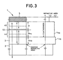
- the organic EL device 1 having a structure wherein the ITO transparent electrode 3, a plurality of organic compound material layers 4 including the light-emitting layer, and the metal electrode 5 are deposited in this order on the glass substrate 2, the organic compound material layers are partitioned with the light-emitting interface 10 of the light-emitting layer into the transparent electrode side portion 4d and the metal electrode side portion 4D.
- the interface between the metal electrode 5 and the organic compound material layer 4D can be regarded as a total-reflecting interface. Accordingly, light traveling from the light-emitting interface 10 of the light-emitting layer to the metal electrode is total-reflected and goes through the light-emitting interface 10, thereby to contribute to external light emission. As a matter of course, most of the light traveling to the transparent electrode 3 contributes to external light emission.
- the interface having the largest refractive index difference in the transparent electrode side portion acts markedly as a reflecting interface.
- the refractive indices of materials used for fabrication of the organic EL device are as follows: the organic compound material layers 4d and 4D: about 1.8; the ITO transparent electrode 3: about 2.0; and the glass (soda-lime glass) substrate 2: about 1.5. Therefore, the difference of refractive index is 0.2 between the organic compound material layer 4d and the ITO transparent electrode 3, and 0.5 between the glass substrate 2 and the transparent electrode 3. The difference of refractive index between the glass substrate 2 and the transparent electrode 3 is largest in the transparent electrode side portion.
- the small difference between the organic compound material layer 4d and the transparent electrode 3 is neglected, and the largest refractive index difference between the glass substrate 2 and the transparent electrode 3 is taken into account.
- the largest refractive index difference can be provided not only between the glass substrate and the transparent electrode, but also within the organic compound material layer 4d, through use of materials having high refractive index deposited therein.
- the main light-traveling route of the light emitted on the light-emitting interface is any one of the following; (1) the light goes from the light-emitting interface directly to the outside, (2) the light is reflected on the metal electrode, comes back to the light-emitting interface, and then goes outside directly, and (3) the light is reflected on the glass, comes back to the light-emitting interface, and goes outside.
- the light-emission efficiency is dependent on the course of interference of light in the cases of (2) and (3) wherein the light comes to the light-emitting interface.
- the preferable design of the film of the organic compound material layer will be described, hereinafter, regarding the light-emitting layer emitting light having a wavelength of ⁇ and serving as a primary component.
- the interference in the light-traveling route (3) of the transparent electrode side portion 4d of the organic compound material layer will be considered.
- the interference enhances the light-emission efficiency. More specifically, the transparent electrode side portion of the organic compound material layer is deposited to have a film thickness such that the optical distance (n org d org + n ITO d ITO ) from the light-emitting interface 10 to the interface of the largest refractive index difference is approximately equal to even multiples of one quarter of the wavelength of ⁇ .
- the interference in the light-traveling route (2) of the metal electrode side portion 4D of the organic compound material layer will be considered.
- a phase difference ⁇ occurs before and after the reflection of light.
- the refractive index is "n" and the film thickness is "D"
- the length of the optical path can be expressed by 2 nD.
- the film thickness "D" of the organic compound material layer 4D When the film thickness "D" of the organic compound material layer 4D is established to be approximately the length of the optical distance, the interference enhances the light-emission efficiency. More specifically, the film thickness "D" of the metal electrode side portion of the organic compound material layer is deposited to have a film thickness such that the optical distance nD from the light-emitting interface 10 to the interface bordering on the metal electrode 5 is approximately equal to odd multiples of one quarter of the wavelength of ⁇ .
- the transparent electrode side portion of the organic compound material layer is formed on the transparent electrode formed on the light-transmitting substrate by depositing one or more of the organic compound material layers, other than the light-emitting layer emitting a light having a wavelength of ⁇ and serving as a primary component, which have a film thickness such that the optical distance from the light-emitting interface of the light-emitting layer to the interface having the largest refractive index difference is approximately equal to even multiples of one quarter of the wavelength of ⁇ .
- the metal electrode side portion of the organic compound material layer is formed on the transparent electrode side portion of the organic compound material layer by depositing the light-emitting layer and the remaining portion the organic compound material layer such that the light-emitting layer and the remaining portion have a film thickness wherein the optical distance from the light-emitting interface of the light-emitting layer to the interface on the metal electrode is approximately equal to odd multiples of one quarter of the wavelength of ⁇ , and then the metal electrode is formed on the metal electrode side portion of the organic compound material layer.
- the element Since the element has the foregoing structure, as the film thickness of the organic compound material layer is gradually increased, the film thickness wherein the phases in the above-described light-traveling routes agree with each other appears one after another. In particular, as the film thickness is increased, the element demonstrates the maximum and minimum values in the light-emission efficiency characteristics with respect to the film thickness of the transparent electrode side portion of the organic compound material layer. In other words, the light-emission efficiency characteristics depend on the total film thickness of the organic compound material layers of the transparent electrode side.
- the film thickness of the organic compound material layer has been established in the vicinity of the first maximum value in the light-emission efficiency characteristics with respect to the film thickness. It has been known that as the film thickness is gradually increased, the light-emission efficiency tends to decrease by degrees.
- the present inventors have found that the element can be enhanced until the element obtains the second maximum value in the efficiency characteristics by increasing the film thickness until the thickness is greater than the thickness bringing the minimum value between the first and second maximum values in the light-emission efficiency characteristics.
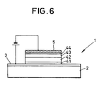
- a plurality of organic EL devices were fabricated by changing the film thickness of the hole-transport layer; they were fabricated, with a transparent electrode (anode) 3/a hole-injection layer 41/a hole-transport layer 42/a light-emitting layer 43/an electron-injection layer 44/a metal electrode (cathode) 5 which were deposited on the substrate 2 in the order.
- Their materials and film thickness were as follows: ITO (110 nm)/MTDATA (25 nm)/TPD (40-200 nm)/aluminum - oxine chelate Alq3 added with quinacridone (60 nm)/aluminum-lithium alloy Al-Li (100 nm).
- the light-emitting layer emits light having a wavelength of 525 nm and serving as a primary component.
- a luminance-current L/I efficiency, a luminance efficiency, and an external quantum efficiency were measured.
- a driving voltage placed at both electrodes of the element applied with a certain current in the forward direction in order for the element to emit light and a withstand voltage i.e., a voltage by which the element comes close to breaking (having a leakage of current) applied with a reverse bias voltage were measured.
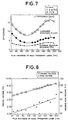
- the results of characteristics of L/I efficiency, luminance efficiency, and external quantum efficiency, respectively with respect to the TPD film thickness, are shown in Fig. 7.
- the characteristics of the driving voltage and withstand voltage, respectively with respect to the TPD film thickness are shown in Fig. 8.
- the first peak is not shown but it is considered to appear in the vicinity of film thickness of 20 nm.
- the minimum peak is known to appear in the vicinity of 100 nm, and the second peak in the vicinity of 180 nm. Accordingly, if the TPD film thickness is increased, the performance of a practical element is obtained by adjusting the thickness such that the high order peak is attained. Consequently, an element having TPD with a film thickness of 120 nm or more, more preferably 170 to 200 nm, is useful as a practical element.
- the film thickness is more than the thickness giving the minimum value between the first and second maximum values in the light-emission efficiency characteristics with respect to the TPD film thickness in the transparent electrode side portion of the organic compound material layer.
- such an element is known to have an increased driving voltage-current and increased withstanding voltage with the increased TPD film thickness and to have a sufficient withstanding voltage in a film thickness of 120 nm or more giving the minimum value between the first and second maximum value in the light-emission efficiency.
- the metal electrode side portion of the organic compound material layer is formed to have a film thickness such that the optical distance from the light-emitting interface of the light-emitting layer to the interface on the metal electrode is approximately equal to odd multiples of one quarter of the wavelength of ⁇ .
- the metal electrode side portion of the organic compound material layer including the light-emitting layer is formed to have a film thickness that is thinner than the established film thickness, as disclosed in Japanese Patent No. 2843924 corresponding to the attenuation characteristics of luminance with respect to the film thickness.
- the interface between the glass substrate 2 and the transparent electrode 3, which is the interface of the largest refractive index difference, is considered to be the reflecting interface.
- a translucent layer is provided between them with the object of using it as a reflecting interface on purpose.
- the film thickness "d" may be established in consideration of the difference of phase ⁇ arising before and after the reflection of light.
- the film thickness of the hole-transport layer may be changed.
- a structure wherein a hole-injection layer is not formed, but a hole-transport layer is formed on the ITO anode may be used.
Landscapes
- Physics & Mathematics (AREA)
- Optics & Photonics (AREA)
- Electroluminescent Light Sources (AREA)
Abstract
Description
wherein the organic compound material layers includes a light-emitting interface of the light-emitting layer demarcating the organic compound material layers and the transparent electrode into a transparent electrode side portion and a metal electrode side portion;
wherein the transparent electrode side portion of the organic compound material layers and the transparent electrode has an interface with a largest difference in refractive indexes thereof; and
wherein the transparent electrode side portion of the organic compound material layer has a film thickness equal to or larger than a thickness corresponding to a minimum value between first and second maximum values of light-emission efficiency in luminescence efficiency characteristics depending on the film thickness of the transparent electrode side portion of the organic compound material layers.
When the total film thickness of the organic
When the film thickness "D" of the organic
Claims (5)
- An organic electroluminescence device comprising a light-transmitting substrate; anda transparent electrode, organic compound material layers including a light-emitting layer and a metal electrode which are formed in this order on the light-transmitting substrate;
wherein the organic compound material layers includes a light-emitting interface of the light-emitting layer demarcating the organic compound material layers and the transparent electrode into a transparent electrode side portion and a metal electrode side portion;
wherein the transparent electrode side portion of the organic compound material layers and the transparent electrode has an interface with a largest difference in refractive indexes thereof; and
wherein the transparent electrode side portion of the organic compound material layer has a film thickness equal to or larger than a thickness corresponding to a minimum value between first and second maximum values of light-emission efficiency in luminescence efficiency characteristics depending on the film thickness of the transparent electrode side portion of the organic compound material layers. - An organic electroluminescence device according to Claim 1, wherein the light-emitting interface of the light-emitting layer emitting light having a wavelength of λ serving as a primary component, and wherein the transparent electrode side portion in the organic compound material layers is deposited to have a film thickness such that an optical distance from the light-emitting interface to the interface with the largest difference in refractive indexes is substantially equal to even multiples of one-quarter of the wavelength λ.
- An organic electroluminescence device according to Claim 2, wherein the metal electrode side portion in the organic compound material layers is deposited to have a film thickness such that an optical distance from the light-emitting interface to an interface bordering on the metal electrode is substantially equal to odd multiples of one quarter of the wavelength λ.
- A process for fabricating an organic electroluminescence device including a light-transmitting substrate; and a transparent electrode, organic compound material layers including a light-emitting layer emitting primarily light with a wavelength of λ and a metal electrode which are formed in this order on the light-transmitting substrate; wherein the organic compound material layers includes a light-emitting interface of the light-emitting layer demarcating the organic compound material layers and the transparent electrode into a transparent electrode side portion and a metal electrode side portion; and wherein the transparent electrode side portion of the organic compound material layers and the transparent electrode has an interface with a largest difference in refractive indexes thereof;the process comprising the steps of:providing a light-transmitting substrate on which a transparent electrode is formed;layering organic compound material layers in turn on the transparent electrode to form a transparent electrode side portion of organic compound material layers so as to have a film thickness such that an optical distance from the light-emitting interface to the interface with the largest difference in the refractive indexes is substantially equal to even multiples of one quarter of the wavelength λ;layering a light-emitting layer and other organic compound material layers in turn on the transparent electrode side portion to form a metal electrode side portion of organic compound material layer so as to have a film thickness such that an optical distance from the light-emitting interface to an interface bordering on the metal electrode is substantially equal to odd multiples of one quarter of the wavelength λ; andlayering a metal electrode on the metal electrode side portion of the organic compound material layer.
- A process for fabricating an organic electroluminescence device according to Claim 4, wherein the organic compound material layers and the metal electrode are deposited by means of vapor deposition.
Applications Claiming Priority (2)
| Application Number | Priority Date | Filing Date | Title |
|---|---|---|---|
| JP3960499 | 1999-02-18 | ||
| JP03960499A JP4001692B2 (en) | 1999-02-18 | 1999-02-18 | Organic electroluminescence device and manufacturing method thereof |
Publications (3)
| Publication Number | Publication Date |
|---|---|
| EP1030382A2 true EP1030382A2 (en) | 2000-08-23 |
| EP1030382A3 EP1030382A3 (en) | 2004-06-09 |
| EP1030382B1 EP1030382B1 (en) | 2009-08-26 |
Family
ID=12557731
Family Applications (1)
| Application Number | Title | Priority Date | Filing Date |
|---|---|---|---|
| EP00101657A Expired - Lifetime EP1030382B1 (en) | 1999-02-18 | 2000-02-01 | Organic electroluminescence device and process for fabricating the same |
Country Status (4)
| Country | Link |
|---|---|
| US (1) | US6505901B1 (en) |
| EP (1) | EP1030382B1 (en) |
| JP (1) | JP4001692B2 (en) |
| DE (1) | DE60042802D1 (en) |
Cited By (4)
| Publication number | Priority date | Publication date | Assignee | Title |
|---|---|---|---|---|
| US7777413B2 (en) | 2005-03-17 | 2010-08-17 | Idemitsu Kosan Co., Ltd. | Organic electroluminescent device having an optical resonator |
| EP1624502A3 (en) * | 2004-08-04 | 2011-04-06 | Semiconductor Energy Laboratory Co., Ltd. | Light-emitting element, display device, and electronic appliance |
| US8269227B2 (en) | 2005-06-09 | 2012-09-18 | Semiconductor Energy Laboratory Co., Ltd. | Light emitting device and electronic device |
| CN103915569A (en) * | 2012-12-28 | 2014-07-09 | 乐金显示有限公司 | Organic light emitting display device and method of manufacturing the same |
Families Citing this family (35)
| Publication number | Priority date | Publication date | Assignee | Title |
|---|---|---|---|---|
| JP2003068472A (en) * | 2001-08-29 | 2003-03-07 | Hitachi Ltd | Organic light emitting device and organic light emitting display using the same |
| TW594617B (en) * | 2002-03-13 | 2004-06-21 | Sanyo Electric Co | Organic EL display panel and method for making the same |
| JP4497881B2 (en) * | 2003-09-30 | 2010-07-07 | 三洋電機株式会社 | Organic EL device and organic EL panel |
| JP4428979B2 (en) * | 2003-09-30 | 2010-03-10 | 三洋電機株式会社 | Organic EL panel |
| JP4716699B2 (en) * | 2003-09-30 | 2011-07-06 | 三洋電機株式会社 | Organic EL panel |
| JP2005197009A (en) * | 2003-12-26 | 2005-07-21 | Sanyo Electric Co Ltd | Display device, manufacturing method thereof, and manufacturing device |
| JP4475942B2 (en) * | 2003-12-26 | 2010-06-09 | 三洋電機株式会社 | Display device and manufacturing method thereof |
| JP4439260B2 (en) * | 2003-12-26 | 2010-03-24 | 三洋電機株式会社 | Manufacturing method of display device |
| TWI272039B (en) * | 2004-06-18 | 2007-01-21 | Sanyo Electric Co | Electroluminescence panel |
| JP2006092936A (en) * | 2004-09-24 | 2006-04-06 | Toyota Industries Corp | Organic EL device |
| US7601988B2 (en) * | 2004-09-24 | 2009-10-13 | Semiconductor Energy Laboratory Co., Ltd. | Light emitting device |
| WO2006085615A1 (en) * | 2005-02-10 | 2006-08-17 | Tohoku Pioneer Corporation | Self-luminous device and self-luminous panel |
| JP2006244712A (en) * | 2005-02-28 | 2006-09-14 | Sanyo Electric Co Ltd | Organic electroluminescent device |
| TW200642524A (en) * | 2005-02-28 | 2006-12-01 | Sanyo Electric Co | Organic electro-luminescence device |
| JP4573672B2 (en) * | 2005-02-28 | 2010-11-04 | 三洋電機株式会社 | Organic EL panel |
| JP2007019487A (en) * | 2005-06-09 | 2007-01-25 | Semiconductor Energy Lab Co Ltd | LIGHT EMITTING DEVICE AND ELECTRONIC DEVICE |
| US8729795B2 (en) * | 2005-06-30 | 2014-05-20 | Semiconductor Energy Laboratory Co., Ltd. | Light emitting device and electronic device |
| JP2007273902A (en) * | 2006-03-31 | 2007-10-18 | Optrex Corp | Organic LED element |
| JP5452853B2 (en) | 2007-08-28 | 2014-03-26 | パナソニック株式会社 | Organic electroluminescence device |
| JP5279240B2 (en) | 2007-11-22 | 2013-09-04 | キヤノン株式会社 | Multicolor display device |
| KR100982412B1 (en) * | 2008-05-29 | 2010-09-15 | (주)에이디에스 | Electro-optical device and its manufacturing method |
| JP5390850B2 (en) | 2008-12-19 | 2014-01-15 | パナソニック株式会社 | Organic electroluminescence device |
| JP5595033B2 (en) * | 2009-12-25 | 2014-09-24 | キヤノン株式会社 | Display device |
| JP5407909B2 (en) | 2010-01-29 | 2014-02-05 | ソニー株式会社 | LIGHT EMITTING ELEMENT, LIGHTING DEVICE, AND DISPLAY DEVICE |
| JP5407907B2 (en) | 2010-01-29 | 2014-02-05 | ソニー株式会社 | LIGHT EMITTING ELEMENT, LIGHTING DEVICE, AND DISPLAY DEVICE |
| JP5676949B2 (en) * | 2010-07-21 | 2015-02-25 | キヤノン株式会社 | Organic EL display device |
| JP2012195226A (en) | 2011-03-17 | 2012-10-11 | Sony Corp | Light emitting element, lighting system and display device |
| CN103608943B (en) | 2011-03-24 | 2016-02-10 | 松下电器产业株式会社 | White light emitting organic electroluminescent element and white light emitting organic electroluminescent panel |
| JP2012204256A (en) | 2011-03-28 | 2012-10-22 | Sony Corp | Light-emitting element, luminaire and display device |
| WO2013190656A1 (en) * | 2012-06-20 | 2013-12-27 | パイオニア株式会社 | Organic electroluminescence element |
| JP2014127303A (en) * | 2012-12-26 | 2014-07-07 | Cbc Kk | Method of manufacturing organic el device |
| JP6114592B2 (en) | 2013-03-21 | 2017-04-12 | 株式会社半導体エネルギー研究所 | Display device, manufacturing method thereof, and electronic apparatus |
| JP6174877B2 (en) | 2013-03-21 | 2017-08-02 | 株式会社半導体エネルギー研究所 | Display device and electronic device |
| KR101809813B1 (en) | 2016-01-14 | 2017-12-15 | 광운대학교 산학협력단 | Self-metered solution-processable organic light-emitting devices based on small molecular emissive layers doped with interface-engineering additives |
| US11917840B2 (en) | 2018-05-18 | 2024-02-27 | Semiconductor Energy Laboratory Co., Ltd. | Light-emitting device with reflective electrode and light-emitting layer |
Family Cites Families (15)
| Publication number | Priority date | Publication date | Assignee | Title |
|---|---|---|---|---|
| EP0443861B2 (en) * | 1990-02-23 | 2008-05-28 | Sumitomo Chemical Company, Limited | Organic electroluminescence device |
| US5093698A (en) * | 1991-02-12 | 1992-03-03 | Kabushiki Kaisha Toshiba | Organic electroluminescent device |
| JP2843924B2 (en) | 1991-06-24 | 1999-01-06 | パイオニア株式会社 | Surface emitting device |
| JPH05307997A (en) * | 1992-04-30 | 1993-11-19 | Pioneer Electron Corp | Organic electroluminescent device |
| JP2846571B2 (en) * | 1994-02-25 | 1999-01-13 | 出光興産株式会社 | Organic electroluminescence device |
| JP3813217B2 (en) | 1995-03-13 | 2006-08-23 | パイオニア株式会社 | Method for manufacturing organic electroluminescence display panel |
| JP3479344B2 (en) * | 1994-08-08 | 2003-12-15 | アヴェンティス・リサーチ・ウント・テクノロジーズ・ゲーエムベーハー・ウント・コー・カーゲー | Organic electroluminescence device |
| US5981092A (en) * | 1996-03-25 | 1999-11-09 | Tdk Corporation | Organic El device |
| EP0818943B1 (en) * | 1996-07-09 | 2005-02-23 | Sony Corporation | Electroluminescent device |
| EP0891121B8 (en) * | 1996-12-28 | 2013-01-02 | Futaba Corporation | Organic electroluminescent elements |
| JPH10270171A (en) * | 1997-01-27 | 1998-10-09 | Junji Kido | Organic electroluminescent device |
| JPH1187068A (en) * | 1997-07-15 | 1999-03-30 | Tdk Corp | Organic EL device and method of manufacturing the same |
| JP2000252074A (en) * | 1998-12-29 | 2000-09-14 | Tdk Corp | Organic EL device |
| US6208076B1 (en) * | 1999-01-13 | 2001-03-27 | Tdk Corporation | Organic electroluminescent device with silicone oxide and/or germanium oxide insulative layer |
| JP4543446B2 (en) * | 1999-04-05 | 2010-09-15 | Tdk株式会社 | Organic EL device |
-
1999
- 1999-02-18 JP JP03960499A patent/JP4001692B2/en not_active Expired - Lifetime
-
2000
- 2000-02-01 EP EP00101657A patent/EP1030382B1/en not_active Expired - Lifetime
- 2000-02-01 DE DE60042802T patent/DE60042802D1/en not_active Expired - Lifetime
- 2000-02-03 US US09/496,951 patent/US6505901B1/en not_active Expired - Lifetime
Cited By (10)
| Publication number | Priority date | Publication date | Assignee | Title |
|---|---|---|---|---|
| EP1624502A3 (en) * | 2004-08-04 | 2011-04-06 | Semiconductor Energy Laboratory Co., Ltd. | Light-emitting element, display device, and electronic appliance |
| US7964891B2 (en) | 2004-08-04 | 2011-06-21 | Semiconductor Energy Laboratory Co., Ltd. | Light-emitting element, display device, and electronic appliance |
| US8618574B2 (en) | 2004-08-04 | 2013-12-31 | Semiconductor Energy Laboratory Co., Ltd. | Light-emitting element, display device, and electronic appliance |
| US7777413B2 (en) | 2005-03-17 | 2010-08-17 | Idemitsu Kosan Co., Ltd. | Organic electroluminescent device having an optical resonator |
| US8269227B2 (en) | 2005-06-09 | 2012-09-18 | Semiconductor Energy Laboratory Co., Ltd. | Light emitting device and electronic device |
| US8461605B2 (en) | 2005-06-09 | 2013-06-11 | Semiconductor Energy Laboratory Co., Ltd. | Light emitting device and electronic device |
| CN103915569A (en) * | 2012-12-28 | 2014-07-09 | 乐金显示有限公司 | Organic light emitting display device and method of manufacturing the same |
| US9735206B2 (en) | 2012-12-28 | 2017-08-15 | Lg Display Co., Ltd. | Organic light emitting display device and method of manufacturing the same |
| US9831291B2 (en) | 2012-12-28 | 2017-11-28 | Lg Display Co., Ltd. | Organic light emitting display device and method of manufacturing the same |
| CN103915569B (en) * | 2012-12-28 | 2018-01-26 | 乐金显示有限公司 | Organic light-emitting display device and its manufacture method |
Also Published As
| Publication number | Publication date |
|---|---|
| JP4001692B2 (en) | 2007-10-31 |
| EP1030382B1 (en) | 2009-08-26 |
| JP2000243573A (en) | 2000-09-08 |
| US6505901B1 (en) | 2003-01-14 |
| DE60042802D1 (en) | 2009-10-08 |
| EP1030382A3 (en) | 2004-06-09 |
Similar Documents
| Publication | Publication Date | Title |
|---|---|---|
| US6505901B1 (en) | Organic electroluminescence device and process for fabricating the same | |
| JP4573672B2 (en) | Organic EL panel | |
| KR100779440B1 (en) | Organic el device | |
| US6406801B1 (en) | Optical resonator type organic electroluminescent element | |
| US7923920B2 (en) | Organic light-emitting elements of LED with light reflection layers in each spaced on opposite sides of transparent conductive layer | |
| US7750559B2 (en) | Organic electroluminescent element array | |
| US20200035770A1 (en) | Display substrate and manufacturing method thereof, and display device | |
| JP4164251B2 (en) | Organic EL color display and manufacturing method thereof | |
| US20040145303A1 (en) | Display device and display unit using the same | |
| WO2000001204A9 (en) | Electroluminescent display | |
| WO2006054137A1 (en) | Organic light emitting device s comprising dielectric capping layers | |
| KR20010107695A (en) | Reduction of ambient-light-reflection in organic light-emitting devices | |
| US20190103587A1 (en) | Organic light emitting diode lighting apparatus | |
| JP2003272855A (en) | Organic EL element and organic EL panel | |
| JP2001338770A (en) | Light emitting display device and method of manufacturing the same | |
| JP4817789B2 (en) | Organic EL display device | |
| JP3242992B2 (en) | Organic electroluminescence device | |
| KR101321956B1 (en) | Organic double-sided light-emitting diode with a light extraction dielectric layer | |
| US7206112B2 (en) | Image display device and manufacuring method | |
| US20160155989A1 (en) | Organic electroluminescent element and lighting device | |
| JP4104339B2 (en) | LIGHT EMITTING ELEMENT, MANUFACTURING METHOD THEREOF, AND DISPLAY DEVICE | |
| JP2006139932A (en) | ORGANIC ELECTROLUMINESCENT ELEMENT AND METHOD FOR PRODUCING ORGANIC ELECTROLUMINESCENT ELEMENT | |
| JP4303011B2 (en) | Top-emitting organic electroluminescence display element and method for manufacturing the same | |
| JPH053081A (en) | Flat luminous device | |
| JP2004152751A (en) | Organic electroluminescence device |
Legal Events
| Date | Code | Title | Description |
|---|---|---|---|
| PUAI | Public reference made under article 153(3) epc to a published international application that has entered the european phase |
Free format text: ORIGINAL CODE: 0009012 |
|
| AK | Designated contracting states |
Kind code of ref document: A2 Designated state(s): AT BE CH CY DE DK ES FI FR GB GR IE IT LI LU MC NL PT SE |
|
| AX | Request for extension of the european patent |
Free format text: AL;LT;LV;MK;RO;SI |
|
| PUAL | Search report despatched |
Free format text: ORIGINAL CODE: 0009013 |
|
| AK | Designated contracting states |
Kind code of ref document: A3 Designated state(s): AT BE CH CY DE DK ES FI FR GB GR IE IT LI LU MC NL PT SE |
|
| AX | Request for extension of the european patent |
Extension state: AL LT LV MK RO SI |
|
| 17P | Request for examination filed |
Effective date: 20040615 |
|
| 17Q | First examination report despatched |
Effective date: 20041112 |
|
| AKX | Designation fees paid |
Designated state(s): DE FR GB |
|
| 17Q | First examination report despatched |
Effective date: 20041112 |
|
| GRAP | Despatch of communication of intention to grant a patent |
Free format text: ORIGINAL CODE: EPIDOSNIGR1 |
|
| RIC1 | Information provided on ipc code assigned before grant |
Ipc: H01L 51/52 20060101AFI20090203BHEP |
|
| GRAS | Grant fee paid |
Free format text: ORIGINAL CODE: EPIDOSNIGR3 |
|
| GRAA | (expected) grant |
Free format text: ORIGINAL CODE: 0009210 |
|
| AK | Designated contracting states |
Kind code of ref document: B1 Designated state(s): DE FR GB |
|
| REG | Reference to a national code |
Ref country code: GB Ref legal event code: FG4D |
|
| REF | Corresponds to: |
Ref document number: 60042802 Country of ref document: DE Date of ref document: 20091008 Kind code of ref document: P |
|
| PLBE | No opposition filed within time limit |
Free format text: ORIGINAL CODE: 0009261 |
|
| STAA | Information on the status of an ep patent application or granted ep patent |
Free format text: STATUS: NO OPPOSITION FILED WITHIN TIME LIMIT |
|
| 26N | No opposition filed |
Effective date: 20100527 |
|
| GBPC | Gb: european patent ceased through non-payment of renewal fee |
Effective date: 20100201 |
|
| REG | Reference to a national code |
Ref country code: FR Ref legal event code: ST Effective date: 20101029 |
|
| PG25 | Lapsed in a contracting state [announced via postgrant information from national office to epo] |
Ref country code: FR Free format text: LAPSE BECAUSE OF NON-PAYMENT OF DUE FEES Effective date: 20100301 |
|
| PG25 | Lapsed in a contracting state [announced via postgrant information from national office to epo] |
Ref country code: GB Free format text: LAPSE BECAUSE OF NON-PAYMENT OF DUE FEES Effective date: 20100201 |
|
| PGFP | Annual fee paid to national office [announced via postgrant information from national office to epo] |
Ref country code: DE Payment date: 20190122 Year of fee payment: 20 |
|
| PGFP | Annual fee paid to national office [announced via postgrant information from national office to epo] |
Ref country code: DE Payment date: 20190122 Year of fee payment: 20 |
|
| REG | Reference to a national code |
Ref country code: DE Ref legal event code: R071 Ref document number: 60042802 Country of ref document: DE |