EP0443861B2 - Organic electroluminescence device - Google Patents
Organic electroluminescence device Download PDFInfo
- Publication number
- EP0443861B2 EP0443861B2 EP91301416A EP91301416A EP0443861B2 EP 0443861 B2 EP0443861 B2 EP 0443861B2 EP 91301416 A EP91301416 A EP 91301416A EP 91301416 A EP91301416 A EP 91301416A EP 0443861 B2 EP0443861 B2 EP 0443861B2
- Authority
- EP
- European Patent Office
- Prior art keywords
- phenylene
- light emitting
- general formula
- organic electroluminescence
- electroluminescence device
- Prior art date
- Legal status (The legal status is an assumption and is not a legal conclusion. Google has not performed a legal analysis and makes no representation as to the accuracy of the status listed.)
- Expired - Lifetime
Links
Images

Classifications
-
- H—ELECTRICITY
- H05—ELECTRIC TECHNIQUES NOT OTHERWISE PROVIDED FOR
- H05B—ELECTRIC HEATING; ELECTRIC LIGHT SOURCES NOT OTHERWISE PROVIDED FOR; CIRCUIT ARRANGEMENTS FOR ELECTRIC LIGHT SOURCES, IN GENERAL
- H05B33/00—Electroluminescent light sources
- H05B33/12—Light sources with substantially two-dimensional [2D] radiating surfaces
- H05B33/14—Light sources with substantially two-dimensional [2D] radiating surfaces characterised by the chemical or physical composition or the arrangement of the electroluminescent material, or by the simultaneous addition of the electroluminescent material in or onto the light source
-
- C—CHEMISTRY; METALLURGY
- C08—ORGANIC MACROMOLECULAR COMPOUNDS; THEIR PREPARATION OR CHEMICAL WORKING-UP; COMPOSITIONS BASED THEREON
- C08G—MACROMOLECULAR COMPOUNDS OBTAINED OTHERWISE THAN BY REACTIONS ONLY INVOLVING UNSATURATED CARBON-TO-CARBON BONDS
- C08G61/00—Macromolecular compounds obtained by reactions forming a carbon-to-carbon link in the main chain of the macromolecule
-
- C—CHEMISTRY; METALLURGY
- C09—DYES; PAINTS; POLISHES; NATURAL RESINS; ADHESIVES; COMPOSITIONS NOT OTHERWISE PROVIDED FOR; APPLICATIONS OF MATERIALS NOT OTHERWISE PROVIDED FOR
- C09K—MATERIALS FOR MISCELLANEOUS APPLICATIONS, NOT PROVIDED FOR ELSEWHERE
- C09K11/00—Luminescent materials, e.g. electroluminescent or chemiluminescent
- C09K11/06—Luminescent materials, e.g. electroluminescent or chemiluminescent containing organic luminescent materials
-
- H—ELECTRICITY
- H10—SEMICONDUCTOR DEVICES; ELECTRIC SOLID-STATE DEVICES NOT OTHERWISE PROVIDED FOR
- H10K—ORGANIC ELECTRIC SOLID-STATE DEVICES
- H10K50/00—Organic light-emitting devices
- H10K50/10—OLEDs or polymer light-emitting diodes [PLED]
- H10K50/11—OLEDs or polymer light-emitting diodes [PLED] characterised by the electroluminescent [EL] layers
-
- H—ELECTRICITY
- H10—SEMICONDUCTOR DEVICES; ELECTRIC SOLID-STATE DEVICES NOT OTHERWISE PROVIDED FOR
- H10K—ORGANIC ELECTRIC SOLID-STATE DEVICES
- H10K85/00—Organic materials used in the body or electrodes of devices covered by this subclass
- H10K85/10—Organic polymers or oligomers
- H10K85/111—Organic polymers or oligomers comprising aromatic, heteroaromatic, or aryl chains, e.g. polyaniline, polyphenylene or polyphenylene vinylene
- H10K85/114—Poly-phenylenevinylene; Derivatives thereof
-
- H—ELECTRICITY
- H10—SEMICONDUCTOR DEVICES; ELECTRIC SOLID-STATE DEVICES NOT OTHERWISE PROVIDED FOR
- H10K—ORGANIC ELECTRIC SOLID-STATE DEVICES
- H10K50/00—Organic light-emitting devices
- H10K50/10—OLEDs or polymer light-emitting diodes [PLED]
- H10K50/14—Carrier transporting layers
-
- H—ELECTRICITY
- H10—SEMICONDUCTOR DEVICES; ELECTRIC SOLID-STATE DEVICES NOT OTHERWISE PROVIDED FOR
- H10K—ORGANIC ELECTRIC SOLID-STATE DEVICES
- H10K50/00—Organic light-emitting devices
- H10K50/10—OLEDs or polymer light-emitting diodes [PLED]
- H10K50/17—Carrier injection layers
-
- H—ELECTRICITY
- H10—SEMICONDUCTOR DEVICES; ELECTRIC SOLID-STATE DEVICES NOT OTHERWISE PROVIDED FOR
- H10K—ORGANIC ELECTRIC SOLID-STATE DEVICES
- H10K85/00—Organic materials used in the body or electrodes of devices covered by this subclass
- H10K85/60—Organic compounds having low molecular weight
- H10K85/615—Polycyclic condensed aromatic hydrocarbons, e.g. anthracene
- H10K85/621—Aromatic anhydride or imide compounds, e.g. perylene tetra-carboxylic dianhydride or perylene tetracarboxylic di-imide
-
- H—ELECTRICITY
- H10—SEMICONDUCTOR DEVICES; ELECTRIC SOLID-STATE DEVICES NOT OTHERWISE PROVIDED FOR
- H10K—ORGANIC ELECTRIC SOLID-STATE DEVICES
- H10K85/00—Organic materials used in the body or electrodes of devices covered by this subclass
- H10K85/60—Organic compounds having low molecular weight
- H10K85/631—Amine compounds having at least two aryl rest on at least one amine-nitrogen atom, e.g. triphenylamine
-
- H—ELECTRICITY
- H10—SEMICONDUCTOR DEVICES; ELECTRIC SOLID-STATE DEVICES NOT OTHERWISE PROVIDED FOR
- H10K—ORGANIC ELECTRIC SOLID-STATE DEVICES
- H10K85/00—Organic materials used in the body or electrodes of devices covered by this subclass
- H10K85/60—Organic compounds having low molecular weight
- H10K85/649—Aromatic compounds comprising a hetero atom
- H10K85/656—Aromatic compounds comprising a hetero atom comprising two or more different heteroatoms per ring
- H10K85/6565—Oxadiazole compounds
Definitions
- the present invention relates to an organic electroluminescence device, and more particularly, to an organic electroluminescence device which can be easily fabricated and used as a light emitting device for various displays.
- the light emitting layer and the charge transport layers were made by vapor depositing an organic substance in vacuum.
- a vapor deposition method is not suitable for mass-production and has a limit In the production of a device having a large area.
- the EL device is used as a back light for illuminating a non-light emitting display such as an LCD, requests have been made to make the area of the EL device larger, and the EL device needs to be made on a large scale.
- low molecular weight organic fluorescent materials such as tris (8-hydroxyquinoline) aluminum and anthracene, which have been used up to now as the light emitting layer, are difficult to make into a thin film by coating when they are independently used without matrix materials.
- the organic EL device made by vapor deposition has a problem in that it has lower light emitting luminance and light emitting efficiency per unit of electric power than other light emitting devices. To solve this problem, the efficiency of charge injection from an electrode needs to be improved to realize a high luminance with a low drive voltage. Furthermore, when the EL device acts as a display, light must be uniformly emitted over a large area. An organic thin film layer constituting the organic EL device has a very thin film thickness of about 1000 angstroms, and thus a problem occurs in that light is liable to be irregularly emitted. This is thought to be caused by an irregular substrate and an uneven electrode.
- the present inventors have found that when a polymer having a short conjugated chain is used as a light emitting material, the polymer can be easily made into a thin film by, for example, a spin coating method or a casting method, and that an EL device having excellent uniformity can be provided by using the polymer, as the result of a study with an attention paid to the fact that conjugated polymers, which have been studied as conducting polymers, include fluorescent materials. It has also been found that a conducting polymer having a sufficiently long conjugaged chain can be used as a charge transport material and can provide an EL device having excellent uniformity.
- a conducting polymer layer which is disposed between a charge transport layer(s) and an electrode of an organic EL device comprising a light emitting layer and the charge transport layer(s), remarkably improves the uniformity of light emission, light emitting efficiency and luminance.
- the present invention seeks to provide an EL device which uses a conjugated polymer as a light emitting layer and has excellent uniformity of light emission, an EL device which uses a conducting polymer as a charge transport layer and has excellent uniformity of light emission over the whole surface of the device, and an EL device which has a specific conducting polymer layer disposed between a charge transport layer and an electrode and has excellent uniformity of light emission, light emitting efficiency, and luminance.
- the present invention additionally provides an organic electroluminescence device having a light emitting layer, a charge transport layer and a conducting buffer layer disposed between a pair of electrodes at least one of which is transparent or semi-transparent; the conducting polymer buffer layer being disposed between the charge transport layer and one of the electrodes and the conducting polymer having a repeating unit of the general formula (2) : -Ar 2 - B- (2) where Ar 2 and B are as defined above, said conducting polymer having an electrical conductivity of 0.1 S/cm or less.
- Figures 1 to 3 show conceptual cross sectional views of examples of the organic electroluminescence devices of the present invention.
- the methods of synthesizing a conducting polymer of general formula (2) are not particularly limited, but, for exmaple, several known methods as described below can be used.
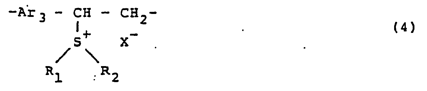
- the thus obtained polymer intermediate having a sulfonium salt as a side chain is reacted with an alcohol to obtain a polymer intermediate having an alkoxy group as a side chain and having a repeating unit of the general formula (5): wherein Ar 3 is as.defined above and R 3 is a hydrocarbon group of 1 to 12 carbon atoms such as methyl, ethyl, propyl or butyl.
- Ar 3 is as.defined above and R 3 is a hydrocarbon group of 1 to 12 carbon atoms such as methyl, ethyl, propyl or butyl.
- the above polymer intermediate having a sulfonium salt as a side chain is reacted with an aromatic sulfonic acid to obtain a polymer intermediate having a sulfonic acid salt as a side chain.
- the conjugated polymer of general formula (1), or the conducting polymer of general formula (2) is very difficult to dissolve in a solvent.
- the polymer intermediates obtained by the above method can, however, be dissolved in a solvent and therefore a solution thereof can be made into a thin film by coating means and subjected to an elimination reaction of their side chains, as described hereinbelow.
- thin films of the conjugated polymers can be prepared.
- the conducting polymer is preferably polyaniline and the derivatives thereof which are obtained by the electrochemical polymerization of aniline or a derivatives thereof, or the chemical polymerization of the same, by a known method.
- the conducting polymer is more preferably polyaniline.
- polyaniline and the derivatives thereof are treated with an alkali solution after they have been polymerized.
- the degree of polymerization of polyaniline and the derivatives thereof is preferably 0.1 dl/g or more in terms of limiting viscosity [ ⁇ ] (in N-methyl-2-pyrrolidone at 30°C).
- Ar 1 in the conjugated polymer of general formula (1) includes, for example, aromatic hydrocarbon groups such as p-phenylene, 2,6-naphthalenediyl and 9,10-anthracenediyl.
- Substituents on the aromatic hydrocarbon group include hydrocarbon groups having 1 to 22 carbon atoms such as methyl, ethyl, propyl, butyl, pentyl, hexyl, heptyl, octyl, lauryl and octadecyl, and alkoxy groups having 1 to 22 carbon atoms such as methoxy, ethoxy, propoxy, pentyloxy, hexyloxy, heptyloxy, octyloxy, lauryloxy and octadecyloxy.
- the nuclear-substituted aromatic group includes mono C 1-22 alkyl-p-phenylene, mono C 1-22 alkoxy-p-phenylene, 2,5-di C 1-22 alkyl-p-phenylene, 2,5-di C 1-22 alkoxy-p-phenylene, more specifically monomethyl-p-phenylene, monomethoxy-p-phenylene, 2,5-dimethyl-p-phenylene, 2,5-dimethoxy-p-phenylene, monoethyl-p-phenylene, 2,5-diethoxy-p-phenylene, 2,5-diethyl-p-phanylene, monobutyl-p-phenylene, monobutoxy-p-phenylene, monobutyl-p-phenylene, 2,5-dibutoxy-p-phenylene, 2.5-diheptyl-p-phenylone, 2,6-diheptyloxy-p-phenylene, 2,5-dioctyl-p-
- p-phenylene, 2,5-di C 1-22 alkyl-p-phenylene and 2,5-di C 1-22 alkoxy-p-phenylene are preferred because the resulting organic EL device has a high light emitting luminance. More preferred are p-phenylene, 2,5-dimethoxy-p-phenylene, 2,5-diethoxy-p-phenylene, 2,5-dibutoxy-p-phenylene, 2,5-diheptyloxy-p-phenylene and 2,5-dilauryloxy-p-phenylene.
- Ar 2 represents a heterocyclic aromatic hydrocarbon group having 4 to 6 carbon atoms containing nitrogen, sulfur or oxygen In addition to an aromatic hydrocarbon group similar to Ar 1 .
- the substituent on the nuclear substituted aromatic hydrocarbon group includes a hydrocarbon group having 1 to 22 carbon atoms and an alkoxy group having 1 to 22 carbon atoms similar to Ar 1 . Specific examples of the nuclear-substituted aromatic group are the same as those of Ar 1 .
- the heterocyclic aromatic hydrocarbon group includes, for example, 2,5-thienylene, 2,5-furandiyl and 2,5-pyrroldiyl.
- the nuclear-substituted heterocyclic aromatic hydrocarbon group having 4 to 6 carbon atoms includes, for example, 2,5-thienylene, 2,5-furandiyl and 2,5-pyrroldiyl having the 3-position and/or the 4-position substituted by the above hydrocarbon group or alkoxy group.
- Preferred are p-phenylene, 2,5-di C 1-22 Alkyl-p-phenylene, 2,5-thienylene, 3-C 1-22 alkyl-2,5-thienylene and 2,5-di C 1-22 alkoxy-2,5-thienylene.
- the molecular weight of their intermediates or the conjugated polymer must be sufficiently high.
- the degree of polymerization is generally 5 or more, preferably 10 to 50000. Specifically, those which have a high molecular weight to be eluted before a solvent elusion position corresponding to a standard polystyrene with a molecular weight of 2800 in the measurement of molecular weights by gel permeation chromatography is more effective.
- the counteranion X - of the sulfonium salt of the polymer intermediate obtained by the monomer of the general formula (3) includes halogen ions such as Cl - and Br and compound ions such as BF 4 - and p-toluene sulfonic acid ions obtained by substituting the halogen ions thereof.
- the polymer intermediate sulfonium salt has a different property depending on the type of the counteranion. When halogen ions are taken as an example, a heat elimination reaction is liable to occur when the counteranion is Br rather than Cl - .
- the counteranion is BF 4 - , the salt is soluble in an organic solvent such as N,N-dimethylformamide.
- the counteranion is a p-toluene sulfonic acid ion, the side chain of the polymer intermediate sulfonium salt may be converted into an alkoxy group.
- a side chain is subjected to an elimination treatment to convert the polymer intermediate into the conjugated polymer.
- the elimination treatment is generally carried out by light exposure or heating, heat treatment is preferable.
- the conjugate chain length can be regulated by the temperature at which the heat treatment is carried out More specifically, at a higher temperature within a predetermined temperature at which the heat treatment is carried out, the longer the conjugate chain is extended.
- the dehydrohalogenation method, and Wittig method are used to make the light emitting material of general formula (1), because these methods can easily control the molecular weight and the conjugate length to obtain a conjugated polymer exhibiting strong fluorescence.
- the conducting polymer of general formula (2) when used for a charge transport layer or a buffer layer, the conducting polymer preferably has a larger molecular weight and a longer conjugate chain.
- the conjugated polymer obtained by the above methods is further subjected to a heat treatment to eliminate side chains not yet eliminated to obtain a material having a better charge transport characteristic.
- the heat treatment temperature is preferably 200°C to 400°C, although it depends on the Ar 2 group in general formula (2).
- the conjugated polymer When the conjugated polymer is used as a charge transport layer or a buffer layer, the polymer intermediate obtained by a sulfonium decomposition method is converted into the conjugated polymer by subjecting it to a heat treatment. It must be fully subjected to the elimination treatment of the side chains for excellent characteristics. The treatment is carried out at 200°C to 400°C.
- the heat treatment time is not particularly limited, so long as a side chain eliminating reaction occurs during the treatment.
- the time is generally 10 minutes to 20 hours, preferably 30 minutes to 8 hours.
- the atmosphere in which the heat treatment is carried out is not particularly limited, so long as the polymer film is not deteriorated and, in particular, an oxidizing reaction is not caused by oxygen and air. It is generally an inert gas atmosphere such as N 2 , Ar or He, or the heat treatment may be carried out in a vacuum or an inert liquid medium.
- the conducting polymer of general formula (2) has an increased electrical conductivity when doped with impurities such as sulfuric acid, iodine or iron (II) chloride. It is also known that, in the state in which the electrical conductivity is increased as described above, absorbance in a visible wavelength region is also increased and optical transmittance is greatly reduced such that transparency is lost Therefore, the doping is not preferably carried out when light emitted is to be taken out from the conducting polymer side of the EL device. Since the absorption spectrum correlates with the electrical conductivity, the electrical conductivity is 0.1 S/cm or less.
- Figures 1, 2 and 3 show the structure of EL devices of the present invention, respectively, when the conjugated polymer of general formula (1) is used as a light emitting material, when the conducting polymer of general formula (2) is used as a charge transport layer, and further when the above conducting polymer is disposed between the charge transport layer and the electrode as a buffer layer.
- a transparent electrode 2 formed on a transparent substrate 1 such as glass or transparent plastic is used as a transparent thin electrode used in a process of manufacturing the EL device.
- a conducting metal oxide film or a semi-transparent metal film are, for example, used as electrode materials.
- the electrode material includes, indium-tin-oxide (ITO), tin oxide (NESA), Au, Pt, Ag and Cu.
- ITO indium-tin-oxide
- NESA tin oxide
- Au gold
- Pt Ag
- Cu copper
- the electrode is made by, for example, a vacuum vapor deposition, sputtering method or plating method, and the film thickness thereof is about 50 angstroms to about 1 micrometer, preferably about 100 angstroms to about 500 angstroms.
- the conjugated polymer of general formula (1) is used as a light emitting layer 3 in the device shown in Figure 1 , a thin film is formed on an electrode 2 from the solution of the polymer or the polymer intermediate thereof.
- the film thickness of the light emitting layer 3 is not particularly limited, it is, for example, 50 angstroms to 10 micrometers, preferably 100 angstoms to 1 micrometer, to increase the current density so as to increase the light emitting efficiency.
- the light emitting layer 3 may be used independently, or further in combination with a known transport material or a light emitting material. More specifically, the light emitting layer may be combined with the charge transport layer of the conducting polymer according to the present invention or a known charge transport layer or a known light emitting layer.
- the conducting polymer of general formula (2) is used as a charge transport layer 5 in the device shown in Figure 2 , a thin film is formed on an electrode from the solution of the polymer or the polymer intermediate thereof.
- the film thickness of the charge transport layer is not particularly limited, it is, for exmaple, 50 angstroms to 10 micrometers, preferably 100 angstoms to 1 micrometer, to increase the current density so as to increase the light emitting efficiency.
- the polymer intermediate is made into a thin film, it is subjected to a heat treatment at 200 to 400°C so that it is sufficiently converted into the corresponding conducting polymer.
- the charge transport layer 5 may be used independently, or a layer of a hole or electron transport material may be further provided therewith.
- the charge transport layer may be combined with the charge transport layer of another conducting polymer according to the present invention or a known charge transport layer Furthermore, a known light emitting layer 3 is formed on the conducting polymer layer 5 and an electron injection, cathode 4 is formed thereon.
- the conducting polymer of general formula (2) is used as a buffer layer 6 disposed between a charge transport layer and an electrode in the device shown In Figure 3 , a thin film is formed on the electrode from the solution of the polymer or the polymer intermediate thereof.
- the film thickness of the buffer layer 6 is not particularly limited, it is, for example, 50 angstroms to 10 micrometers, preferably 100 angstroms to 1 micrometer, more preferably 100 to 1000 angstroms, to increase the current density so as to increase the light emitting efficiency.
- the polymer intermediate is made into a thin film, it is thereafter subjected to a heat treatment at a relatively high temperature of 200 to 400°C so that it is sufficiently converted into the corresponding conducting polymer.
- the conducting polymer layer is used with a hole transport layer 5 as a known charge transport layer and a light emitting layer 3 laminated thereon.
- An electron injection cathode 4 is formed thereto.
- the light emitting layer of the conjugated polymer of general formula (1), the charge transport layer of the conducting polymer of general formula (2) and the buffer layer are made into a thin film by a spin coating method, casting method, dipping method, bar coating method, roll coating method or and vapor deposition to thereby provide a uniform layer having a large area.
- Materials for the known light emitting layer and charge transport layer are not particularly limited.
- Known materials such as those disclosed in, United States Patent Nos. 4,356,429 and 4,539,507 can be used as the light emitting material.
- Preferably used as the light emitting material are, for example, metal complexes of 8-hydroxy quinoline and the derivatives thereof, naphthalene derivatives, anthracene derivatives, perylene derivatives, cyanine dyes, melocyanine dyes, xanthene dyes, cumaline dyes, styryl dyes, other dyes, aromatic amines, tetraphenyl cyclopentadiene derivatives and tetraphenyl butadiene derivatives.
- preferably used are perylene, tris (8-hydroxyquinoline) aluminum (hereinafter referred to as Alq 3 ), tetracene, tetraphenylbutadiene, tetraphenylcyclopentadiene, 9,11-bisstyrylanthracene, 3,3-diethylthiadicarbocyanine-iodine, 1,3-diethyl-5-[(2-(3-ethyl-2-benzothiazolinilidene)-ethylidene]-2-thiohydantoin, 4-dicyanomethylene-6-(p-dimethylaminostyryl)-2-methyl-4H-pyrane, and
- the materials for the known hole transport layer include aromatic amines as listed below: (hereinafter referred to as TAPC), (hereinafter referred to as TPA), and (hereinafter referred to as TPD).
- the structure of the organic EL device may be a combined structure of a so-called sandwich structure having an electron transport layer between a light emitting layer and a cathode as well as the (anode/buffer layer/charge transport layer/light emitting layer/cathode) structure shown in Figure 3 .
- Materials for the electron transport layer in this case include, for example, (hereinafter referred to as PBD).
- PBD photoelectron transport layer
- Alq 3 may be used depending on the combination of the layers.
- the combination of the charge transport layer and light emitting layer may be a bilayer structure of (light emitting layer/charge transport layer) or (charge transport layer/light emitting layer) or alternatively replaced by a three-layer structure of (charge transport layer/light emitting layer/charge transport layer).
- the two charge transport layers may be different from each other.
- These known electron transport layer and light emitting layer are formed by a vacuum vapor deposition method or another known method.
- a spin coating method, casting method, dipping method, bar coating method or roll coating method may, for example be used.
- Preferred materials for the electron injection cathode of the EL device are metals having a small work function which includes Al, In, Mg, Mg-Ag alloy, In-Ag alloy and a graphite thin film.
- the film thickness of the electron injection cathode is 50 angstroms to 1 micrometer, preferably 500 to 6000 angstroms.
- the electron injection cathode is made, for example, by a vacuum vapor deposition method or sputtering method.
- the conjugated polymer which are soluble in a solvent is used as the light emitting material, or the polymer intermediate of the conjugated polymer or the conjugated polymer which are soluble in a solvent is used as the charge transport material or the buffer layer for the electrode, whereby an EL device having a large area can easily be made.
- the buffer layer is used, the uniformity of luminance and light emission is greatly improved.
- EL devices according to the present invention are preferably used as a plane light source such as a back light or flat panel display.
- 2,5-Thienylene bis(dimethylsulfonium bromide) was polymerized using an alkali in the same way as described In Polymer Communication, 28 , 229 (1987) and reacted with methanol to obtain poly(2,5-thienylene methoxyethylene) as a polymer intermediate of poly-2,5-thienylenevinylene(hereinafter referred to as PTV).
- the film thickness of the polymer intermediate was reduced to 400 angstroms by the heat treatment
- an infrared adsorption spectrum was measured, the absorption peak of 1100 cm -1 inherent in the polymer intermediate was found to disappear, and thus a PTV structure was confirmed and the PTV was used as a charge transport layer.
- PPV intermediate poly(p-phenyleneethylene)sulfonium salt
- PPV poly(p-phenylenevinylens
- aqueous solution of the thus obtained PPV intermediate was spin coated at 2000 rpm on a PTV thin film formed on an ITO film. Film thickness at this time was 500 angstoms. Thereafter, the PPV intermediate was subjected to a heat treatment in N 2 at 120°C for 2 hours. The film thickness was 400 angstroms after the heat treatment and it was confirmed by an infrared absorption spectrum that a PPV structure was not perfectly formed and that the structure of the PPV intermediate partially remained. Further, an aluminum electrode was formed thereon similarly to Example 1 to complete a device.
- PAn polyaniline
- Aniline was subjected to chemical oxidation polymerization using ammonium persulfate as an oxidizing agent to obtain polyaniline (hereinafter referred to as PAn), according to the method described in Molecular Crystals and Liquid Crystals, Part E, 121, pp 173 - 180 (1985) . Thereafter, the polyaniline was treated in an aqueous solution of sodium hydroxide, cleaned and dried, and then dissolved in DMF. The DMF solution of PAn was applied to a thickness of 200 angstroms by a spin coating method at 2000 rpm on a glass substrate on which an ITO film thin was deposited to a thickness of 200 angstroms by sputtering, and, thereafter, dried at 200°C for 2 hours.
- perylene was formed on the PAn by a vapor deposition method.
- the degree of vacuum was 5 x 10 -6 Torr (6.7 x 10 -4 Pa) during the deposition and the film thickness of perylene was 1800 angstroms.
- An aluminum electrode was formed thereon by vapor deposition to complete an EL device. When a voltage of 45 V was applied on the device, a current having a current density of 42 mA/cm 2 flowed and a violet EL emitting light having a luminance of 0.11 cd/m 2 was observed. The luminance was in proportion to the current density.
- the poly-2,5-thienylenevinylene intermediate obtained in Example 2 was applied to a thickness of 700 angstroms by a spin coating method at 2000 rpm on a glass substrate on which an ITO thin film was deposited to a thickness of 200 angstroms by sputtering, and, . thereafter, subjected to a heat treatment in N 2 at 200°C for 2 hours.
- the film thickness of the PTV intermediate was reduced to 400 angstroms by the heat treatment.
- Example 2 the chloroform solution of HO-PPV obtained in Example 1 was applied to a thickness of 1000 angstroms by a spin coating method at 2000 rpm on a PTV thin film on which an ITO thin film had been formed, and the resultant material was used as a light emitting material.
- An aluminum electrode was formed thereon by vapor deposition to a thickness of 1000 angstroms. Terminals were formed to the ITO electrode and aluminum electrode using a silver paste and fixed with an epoxy resin.
- a PPV intermediate was applied to a thickness of 600 angstroms by the same method as described in Example 4 except that the PPV intermediate obtained in Example 2 was used in place of the PTV intermediate. Thereafter, the spin coated film of the PPV intermediate was subjected to a heat treatment at 370°C for 2 hours to be made into a PPV thin film. Its film thickness was 300 angstroms after the heat treatment. A change to the PPV structure was confirmed by a change in an infrared absorption spectrum. The PPV thin film was used as a charge transportation film. HO-PPV was spin coated thereon in the same way as in Example 2 and an aluminum electrode was formed by vapor deposition to complete an EL device.
- a PAn film was formed in the same way as in Example 3 and used as a charge transport layer. Further, HO-PPV was spin coated thereon in the same way as in Example 4 and an aluminum electrode was formed by vapor deposition to complete a device.
- a PAn film was formed in the same way as in Example 3 and used as a charge transport layer. Further, an HO-PPV/perylene mixture was applied thereon at 2000 rpm using a chloroform solution of the HO-PPV obtained in Exmaple 1 and perylene of 1 mol% to the HO-PPV dissolved therein, and the resultant material was used as a light emitting layer. Further, an aluminum electrode was formed thereon to a thickness of 1000 angstroms by vapor deposition. Terminals were formed to the ITO electrode and aluminum electrode using a silver paste and fixed with an epoxy resin.
- a PAn film was formed in the same way as in Example 3 and used as a charge transport layer, and . then a chloroform solution of perylene was spin coated thereon at 2000 rpm.
- the HO-PPV obtained in Example 1 was further spin coated at 2000 rpm from its chloroform solution, and finally an aluminum electrode was formed by vapor deposition to a thickness of 1050 angstroms. Terminals were formed to the ITO electrode and aluminum electrode using a silver paste and fixed with an epoxy resin.
- a voltage of 60 V was applied on the thus formed device, a yellow orange light having a luminance of 13 cd/m 2 was observed at a current density of 51 mA/cm 2 .
- a light emitting spectrum had a peak at 580 nm and coincided with that of the HO-PPV.
- An aqueous solution of NaBF 4 was added to an aqueous solution of the PPV intermediate obtained In example 2 to obtain a PPV intermediate with a counter-anion of BF 4 - .
- the thus obtained mixed solution of the PPV/PTV intermediate was spin coated at 2000 rpm to a thickness of 500 angstroms, and, thereafter, subjected to a heat treatment in vacuum at 200°C for 2 hours. The thickness of the coated film was reduced to 300 angstroms by the heat treatment.
- the thin film of the mixture of PTV and PPV was used as a charge transfer layer. .
- Tris (8-quinolinol) aluminum (hereinafter referred to as Alq 3 ) as a light emitting material and indium as an electrode were vapor deposited to a film thickness of 1040 angstroms and 6400 angstroms, respectively. These layers were continuously vapor deposited without breaking the vacuum. The degree of vacuum was 3 x 10 -6 Torr (4x10 -4 Pa) or less when the vapor deposition was carried out. When a voltage of 30 V was applied on the device, a current having a current density of 205 mA/cm 2 flowed and a green EL light having a luminance of 282 cd/m 2 was observed. The luminance was in proportion to the current density.
- the DMF solution of the PTV intermediate obtained in Exmaple 2 was applied to a thickness of 500 angstroms by a spin coating method at 2000 rpm on a commercially available ITO/glass substrate ultra-sonically cleaned in acetone, and, thereafter, subjected to a heat treatment in vacuum at 200°C for 2 hours.
- the film thickness of the PTV intermediate was reduced to 300 angstroms by the heat treatment.
- TPD as a charge transport material
- Alq 3 as a light emitting material
- indium as an electrode
- These layers were continuously vapor deposited without breaking the vacuum.
- the degree of vacuum was 3 x 10 -6 Torr (4x10 -4 Pa) or less when the vacuum deposition was carried out.
- a voltage of 28 V was applied on the device, a current having a current density of 208 mA/cm 2 flowed and a green EL light having a luminance of 3992 cd/m 2 was observed. The luminance was in proportion to the current density.
- Table 1 shows the result of measurement of the characteristics of this device.
- Example 2 An organic EL device was made in the same way as in Example 2 except that the PPV intermediate obtained in Example 2 was used. When a voltage of 35 V was applied on the device, a current having a current density of 190 mA/cm 2 flowed and a green EL light having a luminance of 3395 cd/m 2 was observed. Table 1 shows the result of observation of the light emitting state and the result of measurement of the characteristics of this device, similarly to Example 10.
- a mixed film of PTV and PPV was formed on an ITO/glass substrate in the same way as in Example 10. except that a mixed solution of the polymer intermediates of PPV and PTV obtained in Example 9 was used in place of the PPV intermediate. Next, TPD, Alq 3 and indium were vapor deposited on the thus formed conducting polymer film in the same way as in Example 10, whereby an EL device was made.
- Table 1 shows the result of observation of the light emitting state and the result of measurement of the characteristics of this device, similarly to Example 10.
- a PAn layer was formed to a thickness of 130 angstroms by a spin coating method at 2000 rpm on an ITO-glass substrate from a DMF solution of the PAn obtained in Example 3, and, thereafter, dried in vacuum at 60°C for 2 hours. Further, TPD, Alq 3 and indium were laminated thereon by vacuum vapor deposition similarly to Example 10, whereby an EL device was made.
- Table 1 shows the result of observation of the light emitting state and the result of measurement of the characteristics of this device, similarly to Example 10.
- Example 9 An EL device was made in the same way as in Example 9 except that the conducting polymer layer was not provided. When a voltage of 27 V was applied on the thus made EL device, a green light having a luminance of 3022 cd/m 2 was confirmed at a current density of 185 mA/cm 2 . Table 1 shows the result of observation of the light emitting state and the result of measurement of the characteristics of this device, similarly to Example 10.
- a mixed solution of the PPV and PTV intermediates obtained in Example 9 was applied on an ITO-glass substrate to form a film of the mixture of the PPV and PTV intermediates by a method similar to that used in Example 10 to form the film of the PTV intermediate.
- TPD charge transport material
- TPB tetraphenylbutadiene
- indium as an electrode
- An EL device was made in the same way as in Example 14 except that tetraphenylcyclopentadiene was used in place of TPB. When a voltage of 40 V was applied on the device, a current having a current density of 60 mA/cm 2 flowed and a blue EL light having a luminance of 57 cd/m 2 was observed.
Landscapes
- Chemical & Material Sciences (AREA)
- Organic Chemistry (AREA)
- Engineering & Computer Science (AREA)
- Materials Engineering (AREA)
- Health & Medical Sciences (AREA)
- Chemical Kinetics & Catalysis (AREA)
- Medicinal Chemistry (AREA)
- Polymers & Plastics (AREA)
- Physics & Mathematics (AREA)
- Optics & Photonics (AREA)
- Electroluminescent Light Sources (AREA)
- Luminescent Compositions (AREA)
Description
- The present invention relates to an organic electroluminescence device, and more particularly, to an organic electroluminescence device which can be easily fabricated and used as a light emitting device for various displays.
- Although many trials for fabricating organic electroluminescence devices (hereinafter, referred to as EL devices) have been reported from a viewpoint of the elucidation of the state of electrons in the material thereof, these device have low luminance because it is difficult to inject a carrier into a light emitting layer composed of an organic substance (hereinafter referred to as a light emitting layer) from an electrode. To solve this problem, Tang et al. made a two layer structure composed of a hole transport layer of an organic substance laminated on an organic emitting layer to realize an EL device with high efficiency and high luminance (
United States Patent No. 4,539,507 ). Thereafter, there were made a device comprising a three layer structure having a light emitting layer disposed between an organic electron transport layer and a hole transport layer of an organic substance (hereinafter, these are collectively referred to as charge transport layers) [Japanese Journal of Applied Physics, 27, page 269 (1988)] and EL devices having light emitting layers which are doped with various dyes to give various colors [Journal of Applied Physics, vol. 65, page 3610 (1989)]. - For these organic EL devices reported up to now, the light emitting layer and the charge transport layers were made by vapor depositing an organic substance in vacuum. A vapor deposition method, however, is not suitable for mass-production and has a limit In the production of a device having a large area. Furthermore, when the EL device is used as a back light for illuminating a non-light emitting display such as an LCD, requests have been made to make the area of the EL device larger, and the EL device needs to be made on a large scale. Incidentally, low molecular weight organic fluorescent materials such as tris (8-hydroxyquinoline) aluminum and anthracene, which have been used up to now as the light emitting layer, are difficult to make into a thin film by coating when they are independently used without matrix materials.
- On the other hand, there has been a trial to make a light emitting layer by spin coating a polymer semiconductor such as polyvinylcarbazole in which a fluorescent substance such as perylene or triphenylbutadiene is dispersed [Polymer, 24, 748 (1983)], but this trial has a problem because of low luminance. Therefore, methods for making a thin film for highly luminant EL devices could not help being restricted to limited methods such as a vapor deposition methods.
- The organic EL device made by vapor deposition has a problem in that it has lower light emitting luminance and light emitting efficiency per unit of electric power than other light emitting devices. To solve this problem, the efficiency of charge injection from an electrode needs to be improved to realize a high luminance with a low drive voltage. Furthermore, when the EL device acts as a display, light must be uniformly emitted over a large area. An organic thin film layer constituting the organic EL device has a very thin film thickness of about 1000 angstroms, and thus a problem occurs in that light is liable to be irregularly emitted. This is thought to be caused by an irregular substrate and an uneven electrode.
- The present inventors have found that when a polymer having a short conjugated chain is used as a light emitting material, the polymer can be easily made into a thin film by, for example, a spin coating method or a casting method, and that an EL device having excellent uniformity can be provided by using the polymer, as the result of a study with an attention paid to the fact that conjugated polymers, which have been studied as conducting polymers, include fluorescent materials. It has also been found that a conducting polymer having a sufficiently long conjugaged chain can be used as a charge transport material and can provide an EL device having excellent uniformity. Furthermore the inventors have found that a conducting polymer layer, which is disposed between a charge transport layer(s) and an electrode of an organic EL device comprising a light emitting layer and the charge transport layer(s), remarkably improves the uniformity of light emission, light emitting efficiency and luminance.
- The present invention seeks to provide an EL device which uses a conjugated polymer as a light emitting layer and has excellent uniformity of light emission, an EL device which uses a conducting polymer as a charge transport layer and has excellent uniformity of light emission over the whole surface of the device, and an EL device which has a specific conducting polymer layer disposed between a charge transport layer and an electrode and has excellent uniformity of light emission, light emitting efficiency, and luminance.
- The present invention provides an organic electroluminescence device having a light emitting layer or a light emitting layer and a charge transport layer disposed between a pair of electrodes, at least one of which is transparent or semi-transparent, the light emitting layer comprising a conjugated polymer having a repeating unit of general formula (1):
-Ar1 - CH = CH- (1)
where Ar1 is an aromatic hydrocarbon group of 6 to 14 carbon atoms which is unsubstituted or substituted by one or two hydrocarbon or alkoxy groups having 1 to 22 carbon atoms, said polymer being obtainable by either one of the following methods: - (B) condensation polymerisation in solution, and in the presence of an alkali, of a dihalogenide compound of the general formula (6):
X2 - CH2 - Ar1 - CH2 - X2 (6),
where Ar1 is as defined above and X2 is halogen; - (C) subjecting a dialdehyde compound of general formula:
CHO-Ar1-CHO
where Ar1 is as defined above, and a phosphonium salt of a dihalogenide compound of general formula (6) as defined above to condensation polymerization by a Wittig reaction. - The present invention also provides an organic electroluminescence device having a light emitting layer and a charge transport layer disposed between a pair of electrodes at least one of which is transparent or semi-transparent; the charge transport layer comprising a conducting polymer having a repeating unit of the general formula (2) :
-Ar2 - B- (2)
where Ar2 represents an aromatic hydrocarbon group of 6 to 14 carbon atoms, or a heterocyclic aromatic hydrocarbon group of 4 to 6 carbon atoms containing nitrogen, sulfur or oxygen, which aromatic group is unsubstituted or substituted by one or two hydrocarbon or alkoxy groups of 1 to 22 carbon atoms and B is a -CH = CH- or -NH- group, said conducting polymer having an electrical conductivity of 0.1 S/cm or less. - The present invention additionally provides an organic electroluminescence device having a light emitting layer, a charge transport layer and a conducting buffer layer disposed between a pair of electrodes at least one of which is transparent or semi-transparent; the conducting polymer buffer layer being disposed between the charge transport layer and one of the electrodes and the conducting polymer having a repeating unit of the general formula (2) :
-Ar2 - B- (2)
where Ar2 and B are as defined above, said conducting polymer having an electrical conductivity of 0.1 S/cm or less. -
Figures 1 to 3 show conceptual cross sectional views of examples of the organic electroluminescence devices of the present invention. - The EL device of the present invention will now be described below in more detail.
- The methods of synthesizing a conducting polymer of general formula (2) are not particularly limited, but, for exmaple, several known methods as described below can be used.
- According to the sulfonium salt decomposition method described in
United States Patent No. 4,528,118 , first, a monomer of the general formula (3):
G - CH2 - Ar3 - CH2 - G (3)
wherein Ar3 is as defined for Ar1 or Ar2 described above and G is
The thus obtained polymer intermediate having a sulfonium salt as a side chain is reacted with an alcohol to obtain a polymer intermediate having an alkoxy group as a side chain and having a repeating unit of the general formula (5):
- These three polymer intermediates are subjected to a heat treatment to obtain the conducting polymer of general formula (2) wherein B is -CH = CH-.
- When Ar1, or Ar2 is a non-substituted aromatic hydrocarbon group or is an aromatic hydrocarbon group substituted by alkyl or alkoxy of 3 or less carbon atoms, the conjugated polymer of general formula (1), or the conducting polymer of general formula (2) is very difficult to dissolve in a solvent. The polymer intermediates obtained by the above method can, however, be dissolved in a solvent and therefore a solution thereof can be made into a thin film by coating means and subjected to an elimination reaction of their side chains, as described hereinbelow. Thus, thin films of the conjugated polymers can be prepared.
- When Ar1 or Ar2 is an aromatic hydrocarbon group substituted by alkyl or alkoxy of 4 or more carbon atoms and B is -CH = CH-, the conjugated polymers themselves can be dissolved in a solvent and therefore a dehydrohalogenation method or a Wittig reaction method, can, for example, be applied.
- According to the dehydrohalogenation method, first, a dihalogenide compound of general formula (6):
X2 - CH2 - Ar3 - CH2 - X2 (6)
wherein Ar3 is as defined above and X2 is a halogen, is subjected to condensation polymerization by an alkali such as potassium t-butoxide in solution to obtain the conjugated polymer of general formula (1) or the conducting polymer of general formula (2) wherein B is -CH = CH-. - According to a Wittig reaction method, triphenylphosphine for example, is reacted with a dihalogenide compound of general formula (6) to make a phosphonium salt, and a dialdehyde compound (CHO - Ar3 - CHO) is reacted with the phosphonium salt to obtain the conjugated polymer of general formula (1) or the conducting polymer of general formula (2) wherein B is -CH = CH-.
- When B is -NH- in the conducting polymer of general formula (2), the conducting polymer is preferably polyaniline and the derivatives thereof which are obtained by the electrochemical polymerization of aniline or a derivatives thereof, or the chemical polymerization of the same, by a known method. The conducting polymer is more preferably polyaniline.
- To dissolve the polyaniline and the derivatives thereof in a solvent in high concentrations, they are treated with an alkali solution after they have been polymerized. Sodium hydroxide, potassium hydroxide, aqueous ammonia or hydrazine, for example, can be used as an alkali. The degree of polymerization of polyaniline and the derivatives thereof is preferably 0.1 dl/g or more in terms of limiting viscosity [η] (in N-methyl-2-pyrrolidone at 30°C).
- Ar1 in the conjugated polymer of general formula (1) includes, for example, aromatic hydrocarbon groups such as p-phenylene, 2,6-naphthalenediyl and 9,10-anthracenediyl. Substituents on the aromatic hydrocarbon group include hydrocarbon groups having 1 to 22 carbon atoms such as methyl, ethyl, propyl, butyl, pentyl, hexyl, heptyl, octyl, lauryl and octadecyl, and alkoxy groups having 1 to 22 carbon atoms such as methoxy, ethoxy, propoxy, pentyloxy, hexyloxy, heptyloxy, octyloxy, lauryloxy and octadecyloxy. Therefore, the nuclear-substituted aromatic group includes mono C1-22 alkyl-p-phenylene, mono C1-22 alkoxy-p-phenylene, 2,5-di C1-22 alkyl-p-phenylene, 2,5-di C1-22 alkoxy-p-phenylene, more specifically monomethyl-p-phenylene, monomethoxy-p-phenylene, 2,5-dimethyl-p-phenylene, 2,5-dimethoxy-p-phenylene, monoethyl-p-phenylene, 2,5-diethoxy-p-phenylene, 2,5-diethyl-p-phanylene, monobutyl-p-phenylene, monobutoxy-p-phenylene, monobutyl-p-phenylene, 2,5-dibutoxy-p-phenylene, 2.5-diheptyl-p-phenylone, 2,6-diheptyloxy-p-phenylene, 2,5-dioctyl-p-phenylene, 2,5-dioctyloxy-p-phenylene, 2,5-dilauryl-p-phenylene, 2.5-dilauryloxy-p-phenylene, 2,5-distearyl-p-phenylene and 2,5-distearyloxy-p-phenylene. Among these, p-phenylene, 2,5-di C1-22 alkyl-p-phenylene and 2,5-di C1-22 alkoxy-p-phenylene are preferred because the resulting organic EL device has a high light emitting luminance. More preferred are p-phenylene, 2,5-dimethoxy-p-phenylene, 2,5-diethoxy-p-phenylene, 2,5-dibutoxy-p-phenylene, 2,5-diheptyloxy-p-phenylene and 2,5-dilauryloxy-p-phenylene.
- When B is -CH = CH- in the conducting polymer of general formula (2), Ar2 represents a heterocyclic aromatic hydrocarbon group having 4 to 6 carbon atoms containing nitrogen, sulfur or oxygen In addition to an aromatic hydrocarbon group similar to Ar1. Furthermore, the substituent on the nuclear substituted aromatic hydrocarbon group includes a hydrocarbon group having 1 to 22 carbon atoms and an alkoxy group having 1 to 22 carbon atoms similar to Ar1. Specific examples of the nuclear-substituted aromatic group are the same as those of Ar1. The heterocyclic aromatic hydrocarbon group includes, for example, 2,5-thienylene, 2,5-furandiyl and 2,5-pyrroldiyl. The nuclear-substituted heterocyclic aromatic hydrocarbon group having 4 to 6 carbon atoms includes, for example, 2,5-thienylene, 2,5-furandiyl and 2,5-pyrroldiyl having the 3-position and/or the 4-position substituted by the above hydrocarbon group or alkoxy group. Preferred are p-phenylene, 2,5-di C1-22Alkyl-p-phenylene, 2,5-thienylene, 3-C1-22 alkyl-2,5-thienylene and 2,5-di C1-22 alkoxy-2,5-thienylene.
- More preferred are p-phenylene, 2,5-dimethoxy-p-phenylene, 2,5-diethoxy-p-
phenylene 2,5-dipropoxy-p-phenylene, 2,5-dibutoxy-p-phenylene and 2,5-thienylene. - To obtain a uniform thin film by a spin coating method or a casting method using the conjugated polymer of general formula (1) or the conducting polymer of general formula (2), the molecular weight of their intermediates or the conjugated polymer must be sufficiently high. The degree of polymerization is generally 5 or more, preferably 10 to 50000. Specifically, those which have a high molecular weight to be eluted before a solvent elusion position corresponding to a standard polystyrene with a molecular weight of 2800 in the measurement of molecular weights by gel permeation chromatography is more effective.
- The counteranion X- of the sulfonium salt of the polymer intermediate obtained by the monomer of the general formula (3) includes halogen ions such as Cl- and Br and compound ions such as BF4 - and p-toluene sulfonic acid ions obtained by substituting the halogen ions thereof. The polymer intermediate sulfonium salt has a different property depending on the type of the counteranion. When halogen ions are taken as an example, a heat elimination reaction is liable to occur when the counteranion is Br rather than Cl-. When the counteranion is BF4 -, the salt is soluble in an organic solvent such as N,N-dimethylformamide. When the counteranion is a p-toluene sulfonic acid ion, the side chain of the polymer intermediate sulfonium salt may be converted into an alkoxy group.
- A side chain is subjected to an elimination treatment to convert the polymer intermediate into the conjugated polymer. Although the elimination treatment is generally carried out by light exposure or heating, heat treatment is preferable. When a conjugate chain is formed by subjecting the side chain to heat elimination treatment, the conjugate chain length can be regulated by the temperature at which the heat treatment is carried out More specifically, at a higher temperature within a predetermined temperature at which the heat treatment is carried out, the longer the conjugate chain is extended.
- The dehydrohalogenation method, and Wittig method are used to make the light emitting material of general formula (1), because these methods can easily control the molecular weight and the conjugate length to obtain a conjugated polymer exhibiting strong fluorescence.
- Methods other than the sulfonium salt decomposition method do not need a heat treatment
- On the other hand, when the conducting polymer of general formula (2) is used for a charge transport layer or a buffer layer, the conducting polymer preferably has a larger molecular weight and a longer conjugate chain. The conjugated polymer obtained by the above methods is further subjected to a heat treatment to eliminate side chains not yet eliminated to obtain a material having a better charge transport characteristic. The heat treatment temperature is preferably 200°C to 400°C, although it depends on the Ar2 group in general formula (2).
- When the conjugated polymer is used as a charge transport layer or a buffer layer, the polymer intermediate obtained by a sulfonium decomposition method is converted into the conjugated polymer by subjecting it to a heat treatment. It must be fully subjected to the elimination treatment of the side chains for excellent characteristics. The treatment is carried out at 200°C to 400°C.
- When the conjugated polymer obtained by the sulfonium salt decomposition method is used as a charge transport material or a buffer layer material, the heat treatment time is not particularly limited, so long as a side chain eliminating reaction occurs during the treatment. The time is generally 10 minutes to 20 hours, preferably 30 minutes to 8 hours.
- The atmosphere in which the heat treatment is carried out is not particularly limited, so long as the polymer film is not deteriorated and, in particular, an oxidizing reaction is not caused by oxygen and air. It is generally an inert gas atmosphere such as N2, Ar or He, or the heat treatment may be carried out in a vacuum or an inert liquid medium.
- It is known that the conducting polymer of general formula (2) has an increased electrical conductivity when doped with impurities such as sulfuric acid, iodine or iron (II) chloride. It is also known that, in the state in which the electrical conductivity is increased as described above, absorbance in a visible wavelength region is also increased and optical transmittance is greatly reduced such that transparency is lost Therefore, the doping is not preferably carried out when light emitted is to be taken out from the conducting polymer side of the EL device. Since the absorption spectrum correlates with the electrical conductivity, the electrical conductivity is 0.1 S/cm or less.
-
Figures 1, 2 and 3 show the structure of EL devices of the present invention, respectively, when the conjugated polymer of general formula (1) is used as a light emitting material, when the conducting polymer of general formula (2) is used as a charge transport layer, and further when the above conducting polymer is disposed between the charge transport layer and the electrode as a buffer layer. - A
transparent electrode 2 formed on a transparent substrate 1 such as glass or transparent plastic is used as a transparent thin electrode used in a process of manufacturing the EL device. A conducting metal oxide film or a semi-transparent metal film are, for example, used as electrode materials. - Specifically, the electrode material includes, indium-tin-oxide (ITO), tin oxide (NESA), Au, Pt, Ag and Cu. The electrode is made by, for example, a vacuum vapor deposition, sputtering method or plating method, and the film thickness thereof is about 50 angstroms to about 1 micrometer, preferably about 100 angstroms to about 500 angstroms.
- When the conjugated polymer of general formula (1) is used as a
light emitting layer 3 in the device shown inFigure 1 , a thin film is formed on anelectrode 2 from the solution of the polymer or the polymer intermediate thereof. Although the film thickness of thelight emitting layer 3 is not particularly limited, it is, for example, 50 angstroms to 10 micrometers, preferably 100 angstoms to 1 micrometer, to increase the current density so as to increase the light emitting efficiency. When the polymer intermediate is made into a thin film, it is thereafter subjected to a heat treatment so that it is converted into the corresponding conjugated polymer - The
light emitting layer 3 may be used independently, or further in combination with a known transport material or a light emitting material. More specifically, the light emitting layer may be combined with the charge transport layer of the conducting polymer according to the present invention or a known charge transport layer or a known light emitting layer. - Next, an
electron injection cathode 4 is formed. - When the conducting polymer of general formula (2) is used as a
charge transport layer 5 in the device shown inFigure 2 , a thin film is formed on an electrode from the solution of the polymer or the polymer intermediate thereof. Although the film thickness of the charge transport layer is not particularly limited, it is, for exmaple, 50 angstroms to 10 micrometers, preferably 100 angstoms to 1 micrometer, to increase the current density so as to increase the light emitting efficiency. When the polymer intermediate is made into a thin film, it is subjected to a heat treatment at 200 to 400°C so that it is sufficiently converted into the corresponding conducting polymer. Thecharge transport layer 5 may be used independently, or a layer of a hole or electron transport material may be further provided therewith. More specifically, the charge transport layer may be combined with the charge transport layer of another conducting polymer according to the present invention or a known charge transport layer Furthermore, a knownlight emitting layer 3 is formed on the conductingpolymer layer 5 and an electron injection,cathode 4 is formed thereon. - When the conducting polymer of general formula (2) is used as a buffer layer 6 disposed between a charge transport layer and an electrode in the device shown In
Figure 3 , a thin film is formed on the electrode from the solution of the polymer or the polymer intermediate thereof. Although the film thickness of the buffer layer 6 is not particularly limited, it is, for example, 50 angstroms to 10 micrometers, preferably 100 angstroms to 1 micrometer, more preferably 100 to 1000 angstroms, to increase the current density so as to increase the light emitting efficiency. When the polymer intermediate is made into a thin film, it is thereafter subjected to a heat treatment at a relatively high temperature of 200 to 400°C so that it is sufficiently converted into the corresponding conducting polymer. The conducting polymer layer is used with ahole transport layer 5 as a known charge transport layer and alight emitting layer 3 laminated thereon. Anelectron injection cathode 4 is formed thereto. With this arrangement, the uniformity of light emission over the whole surface of the device, the light emitting efficiency and luminance are remarkably improved. - The light emitting layer of the conjugated polymer of general formula (1), the charge transport layer of the conducting polymer of general formula (2) and the buffer layer are made into a thin film by a spin coating method, casting method, dipping method, bar coating method, roll coating method or and vapor deposition to thereby provide a uniform layer having a large area.
- Materials for the known light emitting layer and charge transport layer are not particularly limited. Known materials such as those disclosed in,
United States Patent Nos. 4,356,429 and4,539,507 can be used as the light emitting material. Preferably used as the light emitting material are, for example, metal complexes of 8-hydroxy quinoline and the derivatives thereof, naphthalene derivatives, anthracene derivatives, perylene derivatives, cyanine dyes, melocyanine dyes, xanthene dyes, cumaline dyes, styryl dyes, other dyes, aromatic amines, tetraphenyl cyclopentadiene derivatives and tetraphenyl butadiene derivatives. Specifically, preferably used are perylene, tris (8-hydroxyquinoline) aluminum (hereinafter referred to as Alq3), tetracene, tetraphenylbutadiene, tetraphenylcyclopentadiene, 9,11-bisstyrylanthracene, 3,3-diethylthiadicarbocyanine-iodine, 1,3-diethyl-5-[(2-(3-ethyl-2-benzothiazolinilidene)-ethylidene]-2-thiohydantoin, 4-dicyanomethylene-6-(p-dimethylaminostyryl)-2-methyl-4H-pyrane,


- The materials for the known hole transport layer include aromatic amines as listed below:


- Note that the structure of the organic EL device may be a combined structure of a so-called sandwich structure having an electron transport layer between a light emitting layer and a cathode as well as the (anode/buffer layer/charge transport layer/light emitting layer/cathode) structure shown in
Figure 3 . Materials for the electron transport layer in this case include, for example,
- In the structure shown in
Figure 3 , the combination of the charge transport layer and light emitting layer may be a bilayer structure of (light emitting layer/charge transport layer) or (charge transport layer/light emitting layer) or alternatively replaced by a three-layer structure of (charge transport layer/light emitting layer/charge transport layer). In the three-layer structure, the two charge transport layers may be different from each other. - These known electron transport layer and light emitting layer are formed by a vacuum vapor deposition method or another known method. When the conjugated polymer and conducting polymer are used, a spin coating method, casting method, dipping method, bar coating method or roll coating method may, for example be used.
- Preferred materials for the electron injection cathode of the EL device are metals having a small work function which includes Al, In, Mg, Mg-Ag alloy, In-Ag alloy and a graphite thin film. The film thickness of the electron injection cathode is 50 angstroms to 1 micrometer, preferably 500 to 6000 angstroms. The electron injection cathode is made, for example, by a vacuum vapor deposition method or sputtering method.
- According to the present invention, the conjugated polymer which are soluble in a solvent is used as the light emitting material, or the polymer intermediate of the conjugated polymer or the conjugated polymer which are soluble in a solvent is used as the charge transport material or the buffer layer for the electrode, whereby an EL device having a large area can easily be made. When the buffer layer is used, the uniformity of luminance and light emission is greatly improved.
- EL devices according to the present invention are preferably used as a plane light source such as a back light or flat panel display.
- The present invention is now further described in the following Examples.
- 9.6 Grams of 2,5-diheptyloxy-p-xylilenedibromide was subjected to condensation polymerization using 5.0 g of potassium t-butoxide in 80 g of xylene to obtain poly-2,5-diheptyloxy-p-phenylenevinylene (HO-PPV). A chloroform solution thereof was applied to a thickness of 1000 angstroms by a spin coating method at 2000 rpm on a glass substrate on which an ITO thin film had been deposited to a thickness of 200 angstroms by sputtering, to provide a light emitting layer. Further, an aluminum electrode was formed thereon to a thickness of 1000 angstroms by vapor deposition. Terminals were formed to the ITO electrode and aluminium electrode using a silver paste and fixed with an epoxy resin.
- When a voltage of 40 V was applied on the thus formed organic EL device, a yellowish orange light having a current density of 2.5 mA/cm2 and a luminance of 0.08 cd/m2 was confirmed. The peak wavelength of the light emitting spectrum was 580 nm and coincided with that of the fluorescent spectrum of the spin-coated thin film of the HO-PPV. Further, the light emitting strength was increased in proportion to the current density.
- 2,5-Thienylene bis(dimethylsulfonium bromide) was polymerized using an alkali in the same way as described In Polymer Communication, 28, 229 (1987) and reacted with methanol to obtain poly(2,5-thienylene methoxyethylene) as a polymer intermediate of poly-2,5-thienylenevinylene(hereinafter referred to as PTV). An N,N-dimethylformamide(hereinafter referred to as DMF) solution of the thus obtained polymer intermediate was applied by a spin coating method at 2000 rpm to a thickness of 700 angstroms on a glass substrate on which an ITO thin film was deposited to a thickness of 200 angstroms by sputtering and, thereafter, subjected to a heat treatment in N2 at 200°C for 2 hours. The film thickness of the polymer intermediate was reduced to 400 angstroms by the heat treatment When an infrared adsorption spectrum was measured, the absorption peak of 1100 cm-1 inherent in the polymer intermediate was found to disappear, and thus a PTV structure was confirmed and the PTV was used as a charge transport layer.
- Next, p-xylilene bis(diethylsulfonium bromide) was polymerized in water by adding dropwise an aqueous solution of sodium hydroxide to obtain an aqueous solution of poly(p-phenyleneethylene)sulfonium salt (hereinafter referred to as PPV intermediate) as a polymer intermediate of poly-p-phenylenevinylens (hereinafter referred to as PPV), according to the description of
United States Patent No. 4,528,118 . - An aqueous solution of the thus obtained PPV intermediate was spin coated at 2000 rpm on a PTV thin film formed on an ITO film. Film thickness at this time was 500 angstoms. Thereafter, the PPV intermediate was subjected to a heat treatment in N2 at 120°C for 2 hours. The film thickness was 400 angstroms after the heat treatment and it was confirmed by an infrared absorption spectrum that a PPV structure was not perfectly formed and that the structure of the PPV intermediate partially remained. Further, an aluminum electrode was formed thereon similarly to Example 1 to complete a device.
- When a voltage of 20 V was applied on the thus formed bilayer laminating type device, a yellow light having a luminance of 0.05 cd/m2 was observed at a current density of 25 mA/cm2. The peak wavelength of a light emitting spectrum was 550 nm and coincided with that of the fluorescent spectrum of the thin film of PPV.
- Aniline was subjected to chemical oxidation polymerization using ammonium persulfate as an oxidizing agent to obtain polyaniline (hereinafter referred to as PAn), according to the method described in Molecular Crystals and Liquid Crystals, Part E, 121, pp 173 - 180 (1985). Thereafter, the polyaniline was treated in an aqueous solution of sodium hydroxide, cleaned and dried, and then dissolved in DMF. The DMF solution of PAn was applied to a thickness of 200 angstroms by a spin coating method at 2000 rpm on a glass substrate on which an ITO film thin was deposited to a thickness of 200 angstroms by sputtering, and, thereafter, dried at 200°C for 2 hours. Next, perylene was formed on the PAn by a vapor deposition method. The degree of vacuum was 5 x 10⁻⁶ Torr (6.7 x 10⁻⁴ Pa) during the deposition and the film thickness of perylene was 1800 angstroms. An aluminum electrode was formed thereon by vapor deposition to complete an EL device. When a voltage of 45 V was applied on the device, a current having a current density of 42 mA/cm2 flowed and a violet EL emitting light having a luminance of 0.11 cd/m2 was observed. The luminance was in proportion to the current density.
- The poly-2,5-thienylenevinylene intermediate obtained in Example 2 was applied to a thickness of 700 angstroms by a spin coating method at 2000 rpm on a glass substrate on which an ITO thin film was deposited to a thickness of 200 angstroms by sputtering, and, . thereafter, subjected to a heat treatment in N2 at 200°C for 2 hours. The film thickness of the PTV intermediate was reduced to 400 angstroms by the heat treatment. When an infrared absorption spectrum was measured, the absorption peak of 1100 cm-1 inherent to the intermediate was found to disppear, and thus a PTV structure was confirmed and the PTV was used as a charge transport material.
- Next, the chloroform solution of HO-PPV obtained in Example 1 was applied to a thickness of 1000 angstroms by a spin coating method at 2000 rpm on a PTV thin film on which an ITO thin film had been formed, and the resultant material was used as a light emitting material. An aluminum electrode was formed thereon by vapor deposition to a thickness of 1000 angstroms. Terminals were formed to the ITO electrode and aluminum electrode using a silver paste and fixed with an epoxy resin.
- When a voltage of 35 V was applied on the thus formed bilayer laminating type device, a yellowish orange light having a luminance of 0.12 cd/m2 was observed at a current density of 7 mA/cm2. The peak wavelength of a light emitting spectrum was 580 nm and coincided with that of the fluorescent spectrum of the thin film of the HO-PPV. Further, the light emitting strength was increased in proportion to the current density.
- A PPV intermediate was applied to a thickness of 600 angstroms by the same method as described in Example 4 except that the PPV intermediate obtained in Example 2 was used in place of the PTV intermediate. Thereafter, the spin coated film of the PPV intermediate was subjected to a heat treatment at 370°C for 2 hours to be made into a PPV thin film. Its film thickness was 300 angstroms after the heat treatment. A change to the PPV structure was confirmed by a change in an infrared absorption spectrum. The PPV thin film was used as a charge transportation film. HO-PPV was spin coated thereon in the same way as in Example 2 and an aluminum electrode was formed by vapor deposition to complete an EL device.
- When a voltage of 30 V was applied on the thus formed bilayer laminating type device, a yellowish orange light having a luminance of 0.09 cd/m2 was observed at a current density of 17 mA/cm2. A light emitting spectrum was similar to that in Example 2.
- A PAn film was formed in the same way as in Example 3 and used as a charge transport layer. Further, HO-PPV was spin coated thereon in the same way as in Example 4 and an aluminum electrode was formed by vapor deposition to complete a device.
- When a voltage of 50 V was applied on the thus formed bilayer laminating type device, a yellowish orange light having a luminance of 0.04 cd/m2 was observed at a current density of 12 mA/cm2. Further, when the applied voltage was increased to provide a current density of 12 mA/cm2, a yellowish orange light having a luminance of 0.43 cd/m2 was confirmed. The light emitting spectrum was similar to that in Example 2.
- A PAn film was formed in the same way as in Example 3 and used as a charge transport layer. Further, an HO-PPV/perylene mixture was applied thereon at 2000 rpm using a chloroform solution of the HO-PPV obtained in Exmaple 1 and perylene of 1 mol% to the HO-PPV dissolved therein, and the resultant material was used as a light emitting layer. Further, an aluminum electrode was formed thereon to a thickness of 1000 angstroms by vapor deposition. Terminals were formed to the ITO electrode and aluminum electrode using a silver paste and fixed with an epoxy resin. When a voltage of 60 V was applied on the thus formed device, a yellow orange light having a luminance of 4 cd/m2 was observed at a current density of 50 mA/cm2. A light emitting spectrum had a peak at 580 nm and coincided with that of the single HO-PPV.
- A PAn film was formed in the same way as in Example 3 and used as a charge transport layer, and . then a chloroform solution of perylene was spin coated thereon at 2000 rpm. The HO-PPV obtained in Example 1 was further spin coated at 2000 rpm from its chloroform solution, and finally an aluminum electrode was formed by vapor deposition to a thickness of 1050 angstroms. Terminals were formed to the ITO electrode and aluminum electrode using a silver paste and fixed with an epoxy resin. When a voltage of 60 V was applied on the thus formed device, a yellow orange light having a luminance of 13 cd/m2 was observed at a current density of 51 mA/cm2. A light emitting spectrum had a peak at 580 nm and coincided with that of the HO-PPV.
- An aqueous solution of NaBF4 was added to an aqueous solution of the PPV intermediate obtained In example 2 to obtain a PPV intermediate with a counter-anion of BF4 -. The PPV intermediate was soluble in DMF and mixed with the PTV intermediate obtained in Example 2 (PPV intermediate/PTV intermediate = 20/80). The thus obtained mixed solution of the PPV/PTV intermediate was spin coated at 2000 rpm to a thickness of 500 angstroms, and, thereafter, subjected to a heat treatment in vacuum at 200°C for 2 hours. The thickness of the coated film was reduced to 300 angstroms by the heat treatment.
- The thin film of the mixture of PTV and PPV was used as a charge transfer layer. .
- Tris (8-quinolinol) aluminum (hereinafter referred to as Alq3) as a light emitting material and indium as an electrode were vapor deposited to a film thickness of 1040 angstroms and 6400 angstroms, respectively. These layers were continuously vapor deposited without breaking the vacuum. The degree of vacuum was 3 x 10⁻⁶ Torr (4x10⁻⁴ Pa) or less when the vapor deposition was carried out. When a voltage of 30 V was applied on the device, a current having a current density of 205 mA/cm2 flowed and a green EL light having a luminance of 282 cd/m2 was observed. The luminance was in proportion to the current density.
- The DMF solution of the PTV intermediate obtained in
Exmaple 2 was applied to a thickness of 500 angstroms by a spin coating method at 2000 rpm on a commercially available ITO/glass substrate ultra-sonically cleaned in acetone, and, thereafter, subjected to a heat treatment in vacuum at 200°C for 2 hours. The film thickness of the PTV intermediate was reduced to 300 angstroms by the heat treatment. When an infrared absorption spectrum was measured, the absorption peak of 1100 cm-1 inherent to the intermediate was found to disappear, and thus the PTV structure was confirmed. - Next, TPD as a charge transport material, Alq3 as a light emitting material, and indium as an electrode were sequentially vapor deposited thereon to a film thickness of 1140 angstroms, 1040 angstroms, and 6400 angstroms, respectively. These layers were continuously vapor deposited without breaking the vacuum. The degree of vacuum was 3 x 10⁻⁶ Torr (4x10⁻⁴ Pa) or less when the vacuum deposition was carried out. When a voltage of 28 V was applied on the device, a current having a current density of 208 mA/cm2 flowed and a green EL light having a luminance of 3992 cd/m2 was observed. The luminance was in proportion to the current density. Further, when observed under a sterecscopic microscope with a magnification of x 8, the light was uniformly emitted over the entire device. Table 1 shows the result of measurement of the characteristics of this device.
- An organic EL device was made in the same way as in Example 2 except that the PPV intermediate obtained in Example 2 was used. When a voltage of 35 V was applied on the device, a current having a current density of 190 mA/cm2 flowed and a green EL light having a luminance of 3395 cd/m2 was observed. Table 1 shows the result of observation of the light emitting state and the result of measurement of the characteristics of this device, similarly to Example 10.
- A mixed film of PTV and PPV was formed on an ITO/glass substrate in the same way as in Example 10. except that a mixed solution of the polymer intermediates of PPV and PTV obtained in Example 9 was used in place of the PPV intermediate. Next, TPD, Alq3 and indium were vapor deposited on the thus formed conducting polymer film in the same way as in Example 10, whereby an EL device was made.
- When a voltage of 25 V was applied on the thus made device, a light having a luminance of 4606 cd/m2 was observed at a current density fo 208 mA/cm2. Table 1 shows the result of observation of the light emitting state and the result of measurement of the characteristics of this device, similarly to Example 10.
- A PAn layer was formed to a thickness of 130 angstroms by a spin coating method at 2000 rpm on an ITO-glass substrate from a DMF solution of the PAn obtained in Example 3, and, thereafter, dried in vacuum at 60°C for 2 hours. Further, TPD, Alq3 and indium were laminated thereon by vacuum vapor deposition similarly to Example 10, whereby an EL device was made.
- When a voltage of 35 V was applied on the thus made device, a green light having a luminance of 4818 cd/m2 was confirmed at a current density of 200 mA/cm2. Table 1 shows the result of observation of the light emitting state and the result of measurement of the characteristics of this device, similarly to Example 10.
- An EL device was made in the same way as in Example 9 except that the conducting polymer layer was not provided. When a voltage of 27 V was applied on the thus made EL device, a green light having a luminance of 3022 cd/m2 was confirmed at a current density of 185 mA/cm2. Table 1 shows the result of observation of the light emitting state and the result of measurement of the characteristics of this device, similarly to Example 10.
- A mixed solution of the PPV and PTV intermediates obtained in Example 9 was applied on an ITO-glass substrate to form a film of the mixture of the PPV and PTV intermediates by a method similar to that used in Example 10 to form the film of the PTV intermediate.
- Next, TPD as a charge transport material, tetraphenylbutadiene (TPB) as a light emitting material, and indium as an electrode were vapor deposited thereon to a film thickness of 1000 angstroms, 500 angstroms, 450 angstroms and 6200 angstroms, respectively. These layers were continuously vapor deposited without breaking the vacuum. The degree of vacuum was 3 x 10⁻⁶ Torr (4x10⁻⁴ Pa) or less when the vapor deposition was carried out.
- When a voltage of 34 V was applied on the device, a current having a current density of 106 mA/cm2 flowed and a blue EL light having a luminance of 960 cd/m2 was observed.
- An EL device was made in the same way as in Example 14 except that tetraphenylcyclopentadiene was used in place of TPB. When a voltage of 40 V was applied on the device, a current having a current density of 60 mA/cm2 flowed and a blue EL light having a luminance of 57 cd/m2 was observed.
Table 1 Example Conducting Polymer Layer (Type) Voltage (V) at 100 cd/m2 Limit Emitting Efficiency at 100 cd/m2 (lm/w) Maximum Luminance (cd/m2) Uniformity of Emitted Light Layer Thickness (Å) Example 8 PTV 16 0.38 3992 B 300 Example 9 PPV 21 0.26 3395 C 120 Example 10 PTV-PPV 13 0.51 4606 B 70 Example 11 PAn 21 0.35 4818 A 100 Comparative Example 1 nil 18 0.25 3022 D A: The entire surface emitted light and no unevenness of the light was found.
B: Although the entire surface emitted light, some unevenness of the light was found.
C: Although almost the entire surface emitted light, bright portions and dark ones existed in the luminance of the light.
D: Most portions were dark, although some portions were bright.
Claims (12)
- An organic electroluminescence device having a light emitting layer or a light emitting layer and a charge transport layer disposed between a pair of electrodes, at least one of which is transparent or semitransparent, the light emitting layer comprising a conjugated polymer having a repeating unit of general formula (1):
-Ar1-CH=CH- (1)
where Ar1 is an aromatic hydrocarbon group of 6 to 14 carbon atoms which is unsubstituted or substituted by one or two hydrocarbon or alkoxy groups of 1 to 22 carbon atoms, said polymer being obtainable by either one of the following methods:(B) condensation polymerisation in solution, and in the presence of an alkali, of a dihalogenide compound of the general formula (6):
X2-CH2-Ar1-CH2-X2 (6)
where Ar1 is as defined above and X2 is halogen;(C) subjecting a dialdehyde compound of general formula:
CHO-Ar1-CHO
where Ar1 is as defined above, and a phosphonium salt of a dihalogenide compound of general formula (6) as defined above to condensation polymerization by a Wittig reaction. - An organic electroluminescence device according to claim 1, wherein Ar1 is p-phenylene, 2,6-naphthalenediyl, 9,10-anthracenediyl, mono C1-22 alkyl-p-phenylene, mono C1-22 alkoxy-p-phenylene, 2,5-di C1-22 alkyl-p-phenylene or 2,5-di C1-22 alkoxy-phenylene.
- An organic electroluminescence device according to claim 2, wherein Ar1 is p-phenylene, 2,5-di C1-22 akyl-p-phenylene or 2,5-di C1-22 alkoxy-p-phenylene.
- An organic electroluminescence device according to claim 3, wherein Ar1 is p-phenylene, 2,5-dimethoxy-p-phenylene, 2,5-diethoxy-p-phenylene, 2,5-dibutoxy-p-phenylene, 2,5-diheptyloxy-p-phenylene or 2,5-dilauryloxy-p-phenylene.
- An organic electroluminescence device having a light emitting layer and a charge transport layer disposed between a pair of electrodes at least one of which is transparent or semi-transparent; the charge transport layer comprising a conducting polymer having a repeating unit of the general formula (2):
-Ar2-B- (2)
where Ar2 represents an aromatic hydrocarbon group of 6 to 14 carbon atoms, or a heterocyclic aromatic hydrocarbon group of 4 to 6 carbon atoms containing nitrogen, sulfur or oxygen, which aromatic group is unsubstituted or substituted by one or two hydrocarbon or alkoxy groups of 1 to 22 carbon atoms and B is a -CH=CH- or -NH-group, said conducting polymer having an electrical conductivity of 0.1 S/cm or less. - An organic electroluminescence device having a light emitting layer, a charge transport layer and a conducting polymer buffer layer disposed between a pair of electrodes at least one of which is transparent or semi-transparent; the conducting polymer buffer layer being disposed between the charge transport layer and one of the electrodes and the conducting polymer having a repeating unit of the general formula (2):
-Ar2-B- (2)
where Ar2 represents an aromatic hydrocarbon group of 6 to 14 carbon atoms, or a heterocyclic aromatic hydrocarbon group of 4 to 6 carbon atoms containing nitrogen, sulfur or oxygen, which aromatic group is unsubstituted or substituted by one or two hydrocarbon or alkoxy groups of 1 to 22 carbon atoms and B represents a -CH=CH- or -NH- group, said conducting polymer having an electrical conductivity of 0.1 S/cm or less. - An organic electroluminescence device according to claim 5 or 6, wherein Ar2 is p-phenylene, mono C1-22 alkyl-p-phenylene, mono C1-22 alkoxy-p-phenylene, 2,5-di C1-22 alkyl-p-phenylene, 2,5-di C1-22 alkoxy-p-phenylene, 2,5-thienylene or 3-C1-22 alkyl-2,5-thienylene, and B is -CH=CH-.
- An organic electroluminescence device according to claim 7, wherein Ar2 is p-phenylene, 2,5-dimethoxy-p-phenylene, 2,5-diethoxy-p-phenylene, 2,5-dipropoxy-p-phenylene, 2,5-dibutoxy-p-phenylene or 2,5-thienylene.
- An organic electroluminescence device according to claim 5 or 6, wherein the conducting polymer is polyaniline.
- An organic electroluminescence device according to claim 5 or 6, wherein said light emitting layer comprises a monomer which is tris(8-hydroxyquinoline) aluminium, tetraphenylbutadiene, tetraphenylcyclopentadiene, perylene, 4-dicyanomethylene-6-(p-dimethylaminostyryl)-2-methyl-4H pyran or 1,3-diethyl-5-[2-(3-ethyl-2-benzothiazolinilidene)ethylidene]-2-thiohydantoin.
- An organic electroluminescence device according to any one of claims 5 to 10, wherein the conducting polymer is obtainable by heat treating at a temperature from 200 to 400°C a polymer intermediate having a repeating unit of general formula (4):


- An organic electroluminescence device according to any one of claims 5 to 10 wherein the conducting polymer is obtainable by condensation polymerisation in solution, and in the presence of an alkali, of a dihalogenide compound of the general formula (6):
X2-CH2-Ar1-CH2-X2 (6)
where Ar1 is as defined in claim 1 and X2 is halogen and then heat treating the resulting product at a temperature of 200 to 400°C.
Applications Claiming Priority (6)
| Application Number | Priority Date | Filing Date | Title |
|---|---|---|---|
| JP2043930A JP2987865B2 (en) | 1990-02-23 | 1990-02-23 | Organic electroluminescence device |
| JP43930/90 | 1990-02-23 | ||
| JP07522590A JP3265395B2 (en) | 1990-03-22 | 1990-03-22 | Organic electroluminescence device |
| JP75225/90 | 1990-03-22 | ||
| JP267870/90 | 1990-10-04 | ||
| JP2267870A JP2998187B2 (en) | 1990-10-04 | 1990-10-04 | Organic electroluminescence device |
Publications (4)
| Publication Number | Publication Date |
|---|---|
| EP0443861A2 EP0443861A2 (en) | 1991-08-28 |
| EP0443861A3 EP0443861A3 (en) | 1992-03-11 |
| EP0443861B1 EP0443861B1 (en) | 1995-07-05 |
| EP0443861B2 true EP0443861B2 (en) | 2008-05-28 |
Family
ID=27291722
Family Applications (1)
| Application Number | Title | Priority Date | Filing Date |
|---|---|---|---|
| EP91301416A Expired - Lifetime EP0443861B2 (en) | 1990-02-23 | 1991-02-22 | Organic electroluminescence device |
Country Status (3)
| Country | Link |
|---|---|
| US (2) | US5317169A (en) |
| EP (1) | EP0443861B2 (en) |
| DE (1) | DE69110922T2 (en) |
Families Citing this family (252)
| Publication number | Priority date | Publication date | Assignee | Title |
|---|---|---|---|---|
| US6331356B1 (en) * | 1989-05-26 | 2001-12-18 | International Business Machines Corporation | Patterns of electrically conducting polymers and their application as electrodes or electrical contacts |
| US5408109A (en) | 1991-02-27 | 1995-04-18 | The Regents Of The University Of California | Visible light emitting diodes fabricated from soluble semiconducting polymers |
| GB9201240D0 (en) * | 1992-01-21 | 1992-03-11 | Lynxvale Ltd | Conjugated polymer |
| GB9215928D0 (en) * | 1992-07-27 | 1992-09-09 | Cambridge Display Tech Ltd | Manufacture of electroluminescent devices |
| GB9215929D0 (en) * | 1992-07-27 | 1992-09-09 | Cambridge Display Tech Ltd | Electroluminescent devices |
| US5352906A (en) * | 1993-01-29 | 1994-10-04 | Iowa State University Research Foundation, Inc. | Poly (p-phenyleneneacetylene) light-emitting diodes |
| US5334539A (en) * | 1993-01-29 | 1994-08-02 | Iowa State University Research Foundation, Inc. | Fabrication of poly(p-phenyleneacetylene) light-emitting diodes |
| CA2122328C (en) * | 1993-04-28 | 1999-01-19 | Hideyuki Murata | Thin-film electroluminescent device |
| US5637652A (en) * | 1993-06-04 | 1997-06-10 | Showa Denko Kabushiki Kaisha | Electroconductive polymer and process for producing the same |
| US5589320A (en) * | 1993-07-21 | 1996-12-31 | Sumitomo Chemical Company, Limited | Polymeric fluorescent substance and organic electroluminescence devices using the same |
| DE4325885A1 (en) * | 1993-08-02 | 1995-02-09 | Basf Ag | Electroluminescent arrangement |
| JP3534445B2 (en) * | 1993-09-09 | 2004-06-07 | 隆一 山本 | EL device using polythiophene |
| DE69433830T2 (en) * | 1993-09-14 | 2005-06-16 | Covion Organic Semiconductors Gmbh | Process for the preparation of polymers of alpha-omega-unsaturated compounds and the resulting high molecular weight conjugated polymers |
| DE4331401A1 (en) * | 1993-09-15 | 1995-03-16 | Hoechst Ag | Use of polymers with isolated chromophores as electroluminescent materials |
| US5723873A (en) * | 1994-03-03 | 1998-03-03 | Yang; Yang | Bilayer composite electrodes for diodes |
| DE69507437T2 (en) * | 1994-05-19 | 1999-07-08 | Koninklijke Philips Electronics N.V., Eindhoven | LIGHT-EMITTING DIODE WITH AN ACTIVE LAYER OF 2.5-SUBSTITUTED POLY (P-PHENYLENE-VINYLENE) |
| DE4422670A1 (en) * | 1994-06-30 | 1996-01-04 | Hoechst Ag | Conjugated polymers with partial structures and their use as electroluminescent materials |
| SE503039C2 (en) * | 1994-07-19 | 1996-03-11 | Forskarpatent I Linkoeping Ab | Electroluminescent device and method of manufacture thereof |
| DE4431039A1 (en) * | 1994-09-01 | 1996-03-07 | Hoechst Ag | Poly (4,5,9,10-tetrahydropyrene-2,7-diyl) derivatives and their use as electroluminescent materials |
| US5546413A (en) * | 1994-09-01 | 1996-08-13 | Motorola | Integrated light emitting device |
| US5665857A (en) * | 1994-09-12 | 1997-09-09 | Motorola | Conjugated polymer with built-in fluorescent centers and method of manufacture |
| DE69514604T2 (en) * | 1994-10-04 | 2000-06-21 | Aventis Research & Technologies Gmbh & Co Kg | Process for the preparation of polymers from alpha, omega unsaturated conjugated compounds |
| DE4442052A1 (en) * | 1994-11-25 | 1996-05-30 | Hoechst Ag | Conjugated polymers with hetero-spiroatoms and their use as electroluminescent materials |
| EP0800563B1 (en) | 1994-12-28 | 2000-07-12 | Cambridge Display Technology Limited | Polymers for use in optical devices |
| US6559256B2 (en) * | 1994-12-28 | 2003-05-06 | Cambridge Display Technology Ltd. | Polymers for use in optical devices |
| DE19500912A1 (en) * | 1995-01-13 | 1996-07-18 | Basf Ag | Electroluminescent arrangement |
| TW334474B (en) † | 1995-02-01 | 1998-06-21 | Sumitomo Kagaku Kk | Method for making a polymeric fluorescent substrate and organic electrolumninescent element |
| DE19505942A1 (en) | 1995-02-21 | 1996-08-22 | Bayer Ag | (Co) polymers based on vinyl units and their use in electroluminescent arrangements |
| US6075106A (en) * | 1995-03-29 | 2000-06-13 | D-51368 Bayer Ag | (Co)polymers based on vinyl units and use thereof in electroluminescent devices |
| DE19511484A1 (en) * | 1995-03-29 | 1996-10-02 | Bayer Ag | (Co) polymers based on vinyl units and their use in electroluminescent arrangements |
| DE19516922A1 (en) * | 1995-05-09 | 1996-11-14 | Bosch Gmbh Robert | Electroluminescent layer system |
| US5719467A (en) * | 1995-07-27 | 1998-02-17 | Hewlett-Packard Company | Organic electroluminescent device |
| WO1997006223A1 (en) * | 1995-08-03 | 1997-02-20 | Philips Electronics N.V. | Electroluminescent device |
| US6310436B1 (en) | 1995-09-22 | 2001-10-30 | Gl Displays, Inc. | Cold cathode fluorescent lamp and display |
| DE19536843A1 (en) * | 1995-10-02 | 1997-04-03 | Bayer Ag | (Co) polymers based on vinyl units and their use in electroluminescent arrangements |
| US5763636A (en) * | 1995-10-12 | 1998-06-09 | Hoechst Aktiengesellschaft | Polymers containing spiro atoms and methods of using the same as electroluminescence materials |
| JP2734442B2 (en) * | 1996-01-30 | 1998-03-30 | 日本電気株式会社 | Thin film EL device and method of manufacturing the same |
| US5929194A (en) * | 1996-02-23 | 1999-07-27 | The Dow Chemical Company | Crosslinkable or chain extendable polyarylpolyamines and films thereof |
| US5798170A (en) * | 1996-02-29 | 1998-08-25 | Uniax Corporation | Long operating life for polymer light-emitting diodes |
| DE19615128A1 (en) * | 1996-04-17 | 1997-10-30 | Hoechst Ag | Conjugated polymers with hetero-spiroatoms and their use as electroluminescent materials |
| GB9609282D0 (en) | 1996-05-03 | 1996-07-10 | Cambridge Display Tech Ltd | Protective thin oxide layer |
| US5989945A (en) * | 1996-05-15 | 1999-11-23 | Seiko Epson Corporation | Thin film device provided with coating film, liquid crystal panel and electronic device, and method for making the thin film device |
| DE19627070A1 (en) | 1996-07-05 | 1998-01-08 | Bayer Ag | Electroluminescent devices using glare systems |
| DE19627071A1 (en) * | 1996-07-05 | 1998-01-08 | Bayer Ag | Electroluminescent devices |
| DE19628119A1 (en) * | 1996-07-12 | 1998-01-29 | Univ Bayreuth Vertreten Durch | Light-emitting apparatus |
| US5902688A (en) * | 1996-07-16 | 1999-05-11 | Hewlett-Packard Company | Electroluminescent display device |
| DE69710781T2 (en) | 1996-07-29 | 2002-10-31 | Cambridge Display Tech | ELECTROLUMINESCENT ARRANGEMENTS WITH ELECTRODE PROTECTION |
| WO1998004610A1 (en) | 1996-07-29 | 1998-02-05 | Cambridge Display Technology Limited | Conjugated copolymers for use in luminescent devices |
| US5728801A (en) * | 1996-08-13 | 1998-03-17 | The Dow Chemical Company | Poly (arylamines) and films thereof |
| DE19632949A1 (en) * | 1996-08-16 | 1998-02-19 | Bayer Ag | (Co) polymers based on vinyl units and their use in electroluminescent arrangements |
| US6207301B1 (en) | 1996-08-21 | 2001-03-27 | Sumitomo Chemical Company, Limited | Polymer fluorescent substance and organic electroluminescence device |
| US5948552A (en) * | 1996-08-27 | 1999-09-07 | Hewlett-Packard Company | Heat-resistant organic electroluminescent device |
| ATE247372T1 (en) | 1996-09-04 | 2003-08-15 | Cambridge Display Tech Ltd | LIGHT EMITTING ORGANIC DEVICES WITH IMPROVED CATHODE |
| JP3813990B2 (en) | 1996-09-04 | 2006-08-23 | ケンブリッジ ディスプレイ テクノロジー リミテッド | Organic light emitting device and method for manufacturing the same |
| US20020075422A1 (en) * | 1996-09-19 | 2002-06-20 | Seiko Epson Corporation | Matrix type display device and manufacturing method thereof |
| EP0862156B1 (en) * | 1996-09-19 | 2005-04-20 | Seiko Epson Corporation | Method of production of a matrix type display device |
| JP3899566B2 (en) * | 1996-11-25 | 2007-03-28 | セイコーエプソン株式会社 | Manufacturing method of organic EL display device |
| DE19652261A1 (en) | 1996-12-16 | 1998-06-18 | Hoechst Ag | Aryl-substituted poly (p-arylenevinylenes), process for their preparation and their use in electroluminescent devices |
| US6452218B1 (en) | 1997-06-10 | 2002-09-17 | Uniax Corporation | Ultra-thin alkaline earth metals as stable electron-injecting electrodes for polymer light emitting diodes |
| GB9713074D0 (en) * | 1997-06-21 | 1997-08-27 | Cambridge Display Tech Ltd | Electrically-conducting colour filters for use in organic light-emitting displays |
| US5998045A (en) * | 1997-07-03 | 1999-12-07 | International Business Machines Corporation | Polymeric light-emitting device |
| US6843937B1 (en) * | 1997-07-16 | 2005-01-18 | Seiko Epson Corporation | Composition for an organic EL element and method of manufacturing the organic EL element |
| US6403236B1 (en) * | 1997-09-04 | 2002-06-11 | Sumitomo Chemical Company, Limited | Polymer light emitting device |
| CN1280708A (en) * | 1997-10-17 | 2001-01-17 | 加利福尼亚大学董事会 | Process for fabricating organic semiconductor devices using ink-jet printing technology and device and system employing same |
| US5945502A (en) * | 1997-11-13 | 1999-08-31 | Xerox Corporation | Electroluminescent polymer compositions and processes thereof |
| US5879821A (en) * | 1997-11-13 | 1999-03-09 | Xerox Corporation | Electroluminescent polymer compositions and processes thereof |
| US6209118B1 (en) * | 1998-01-21 | 2001-03-27 | Micron Technology, Inc. | Method for modifying an integrated circuit |
| GB9805476D0 (en) * | 1998-03-13 | 1998-05-13 | Cambridge Display Tech Ltd | Electroluminescent devices |
| DE19812259A1 (en) | 1998-03-20 | 1999-10-21 | Bayer Ag | EL arrangement based on tertiary amines, alcohol-soluble Alq3 derivatives or mixtures and polymeric binders |
| TW521537B (en) * | 1998-05-08 | 2003-02-21 | Idemitsu Kosan Co | Organic electroluminescence element |
| DE19825765A1 (en) | 1998-06-09 | 1999-12-16 | Bayer Ag | Electroluminescent devices using glare systems |
| CA2276808A1 (en) | 1998-07-04 | 2000-01-04 | Bayer Aktiengesellschaft | Electroluminescent assemblies using boron chelates of 8-aminoquinoline derivatives |
| US6316130B1 (en) | 1998-07-04 | 2001-11-13 | Bayer Aktiengesellschaft | Electroluminescent assemblies using azomethine-metal complexes |
| DE19829947A1 (en) | 1998-07-04 | 2000-01-05 | Bayer Ag | Electroluminescent devices with boron chelates |
| KR100635429B1 (en) * | 1998-08-03 | 2006-10-18 | 듀폰 디스플레이즈, 인크. | Encapsulation of Polymer-Based Solid Devices Using Inorganic Materials |
| DE19839946A1 (en) | 1998-09-02 | 2000-03-09 | Bayer Ag | Electroluminescent devices with multinuclear metal complexes |
| DE19839947A1 (en) | 1998-09-02 | 2000-03-09 | Bayer Ag | Electroluminescent devices with thiophene carboxylate metal complexes |
| DE19840943A1 (en) | 1998-09-08 | 2000-03-09 | Aventis Res & Tech Gmbh & Co | Process for the preparation of derivatives of 4-alkylsulfinylmethylarylenemethanol |
| EP1133803A1 (en) | 1998-10-14 | 2001-09-19 | Uniax Corporation | Thin metal-oxide layer as stable electron-injecting electrode for light emitting diodes |
| US6351067B2 (en) * | 1999-01-21 | 2002-02-26 | City University Of Hong Kong | Organic electroluminescent device with improved hole injecting structure |
| JP4001692B2 (en) * | 1999-02-18 | 2007-10-31 | パイオニア株式会社 | Organic electroluminescence device and manufacturing method thereof |
| JP4258583B2 (en) * | 1999-02-23 | 2009-04-30 | 淳二 城戸 | Electroluminescent device |
| JP4375502B2 (en) * | 1999-02-23 | 2009-12-02 | 淳二 城戸 | Light emitting element |
| NO314525B1 (en) * | 1999-04-22 | 2003-03-31 | Thin Film Electronics Asa | Process for the preparation of organic semiconductor devices in thin film |
| US6849869B1 (en) | 1999-07-19 | 2005-02-01 | Dupont Displays, Inc. | Long lifetime polymer light-emitting devices with improved luminous efficiency and improved radiance |
| US6414104B1 (en) | 1999-07-20 | 2002-07-02 | Sri International | Arylamine-substituted poly (arylene vinylenes) and associated methods of preparation and use |
| US6593690B1 (en) * | 1999-09-03 | 2003-07-15 | 3M Innovative Properties Company | Large area organic electronic devices having conducting polymer buffer layers and methods of making same |
| US6611096B1 (en) * | 1999-09-03 | 2003-08-26 | 3M Innovative Properties Company | Organic electronic devices having conducting self-doped polymer buffer layers |
| US6515433B1 (en) | 1999-09-11 | 2003-02-04 | Coollite International Holding Limited | Gas discharge fluorescent device |
| DE19953806A1 (en) | 1999-11-09 | 2001-05-10 | Covion Organic Semiconductors | Substituted poly (arylenevinylene), process for its manufacture and its use in electroluminescent devices |
| JP3571977B2 (en) | 1999-11-12 | 2004-09-29 | キヤノン株式会社 | Organic light emitting device |
| JP4407776B2 (en) * | 1999-12-02 | 2010-02-03 | 淳二 城戸 | Electroluminescent device |
| JP3503579B2 (en) * | 1999-12-08 | 2004-03-08 | 日本電気株式会社 | Organic EL device and manufacturing method thereof |
| US6537607B1 (en) | 1999-12-17 | 2003-03-25 | Texas Instruments Incorporated | Selective deposition of emissive layer in electroluminescent displays |
| US7357990B2 (en) | 1999-12-20 | 2008-04-15 | Sumitomo Chemical Company, Limited | Polymeric fluorescent material, process for producing the same, and polymeric luminiscent element |
| JP4940493B2 (en) * | 1999-12-20 | 2012-05-30 | 住友化学株式会社 | Polymer phosphor, method for producing the same, and polymer light emitting device |
| JP3754856B2 (en) | 2000-01-27 | 2006-03-15 | キヤノン株式会社 | Organic light emitting device |
| JP3587361B2 (en) | 2000-01-27 | 2004-11-10 | キヤノン株式会社 | Organic light emitting device |
| TW572990B (en) * | 2000-03-16 | 2004-01-21 | Sumitomo Chemical Co | Polymeric fluorescent substance, polymeric fluorescent substance solution and polymer light-emitting device using the same substance |
| US6461749B2 (en) | 2000-03-31 | 2002-10-08 | Canon Kabushiki Kaisha | Organic boron compound, process for producing the compound and organic luminescence device using the compound |
| US6794229B2 (en) | 2000-04-28 | 2004-09-21 | Semiconductor Energy Laboratory Co., Ltd. | Manufacturing method for semiconductor device |
| US20020121638A1 (en) | 2000-06-30 | 2002-09-05 | Vladimir Grushin | Electroluminescent iridium compounds with fluorinated phenylpyridines, phenylpyrimidines, and phenylquinolines and devices made with such compounds |
| US20030129299A1 (en) * | 2000-11-16 | 2003-07-10 | Swanson Leland S. | Selective deposition of emissive layer in electroluminescent displays |
| GB0028317D0 (en) * | 2000-11-21 | 2001-01-03 | South Bank Univ Entpr Ltd | Electroluminescent device incorporating polyaniline |
| DE10063721A1 (en) * | 2000-12-20 | 2002-07-11 | Merck Patent Gmbh | Organic semiconductor, manufacturing process therefor and uses |
| JP3870102B2 (en) * | 2001-02-22 | 2007-01-17 | キヤノン株式会社 | Organic light emitting device |
| EP1382075A1 (en) * | 2001-04-17 | 2004-01-21 | Koninklijke Philips Electronics N.V. | Led comprising a conductive transparent polymer layer with low sulfate and high metal ion content |
| WO2002087287A1 (en) * | 2001-04-19 | 2002-10-31 | Hitachi,Ltd. | Electroluminescence display panel, image display, and method for manufacturing them |
| JP4240841B2 (en) | 2001-04-27 | 2009-03-18 | キヤノン株式会社 | Organic light emitting device |
| US6723828B2 (en) | 2001-05-23 | 2004-04-20 | Sri International | Conjugated electroluminescent polymers and associated methods of preparation and use |
| WO2003020847A1 (en) * | 2001-09-03 | 2003-03-13 | Canon Kabushiki Kaisha | Organic luminescence device |
| JP4235550B2 (en) * | 2001-09-28 | 2009-03-11 | キヤノン株式会社 | Organic light emitting device |
| US7112368B2 (en) * | 2001-11-06 | 2006-09-26 | E. I. Du Pont De Nemours And Company | Poly(dioxythiophene)/poly(acrylamidoalkyslufonic acid) complexes |
| US7250512B2 (en) | 2001-11-07 | 2007-07-31 | E. I. Du Pont De Nemours And Company | Electroluminescent iridium compounds having red-orange or red emission and devices made with such compounds |
| EP2299785A1 (en) | 2001-12-26 | 2011-03-23 | E. I. du Pont de Nemours and Company | Iridium compounds |
| US6955773B2 (en) * | 2002-02-28 | 2005-10-18 | E.I. Du Pont De Nemours And Company | Polymer buffer layers and their use in light-emitting diodes |
| US7204940B2 (en) | 2002-03-20 | 2007-04-17 | Michigan Biotechnology Institute | Conductive polymer-based material |
| JP3848262B2 (en) * | 2002-03-27 | 2006-11-22 | キヤノン株式会社 | Oligofluorenylene compound and organic light-emitting device |
| US7205366B2 (en) * | 2002-04-02 | 2007-04-17 | E. I. Du Pont De Nemours And Company | Hole transport polymers and devices made with such polymers |
| JP3919583B2 (en) * | 2002-04-12 | 2007-05-30 | キヤノン株式会社 | Organic light emitting device |
| US7090929B2 (en) | 2002-07-30 | 2006-08-15 | E.I. Du Pont De Nemours And Company | Metallic complexes covalently bound to conjugated polymers and electronic devices containing such compositions |
| US6784017B2 (en) * | 2002-08-12 | 2004-08-31 | Precision Dynamics Corporation | Method of creating a high performance organic semiconductor device |
| US20040092700A1 (en) * | 2002-08-23 | 2004-05-13 | Che-Hsiung Hsu | Methods for directly producing stable aqueous dispersions of electrically conducting polyanilines |
| JP4585750B2 (en) | 2002-08-27 | 2010-11-24 | キヤノン株式会社 | Fused polycyclic compound and organic light emitting device using the same |
| JP3848224B2 (en) * | 2002-08-27 | 2006-11-22 | キヤノン株式会社 | Spiro compound and organic light emitting device using the same |
| JP3902993B2 (en) * | 2002-08-27 | 2007-04-11 | キヤノン株式会社 | Fluorene compound and organic light emitting device using the same |
| JP4164317B2 (en) * | 2002-08-28 | 2008-10-15 | キヤノン株式会社 | Organic light emitting device |
| JP4311707B2 (en) * | 2002-08-28 | 2009-08-12 | キヤノン株式会社 | Organic light emitting device |
| JP4125076B2 (en) * | 2002-08-30 | 2008-07-23 | キヤノン株式会社 | Monoaminofluorene compound and organic light-emitting device using the same |
| JP4208526B2 (en) * | 2002-09-12 | 2009-01-14 | キヤノン株式会社 | ORGANIC EL DISPLAY DEVICE AND ELECTRONIC DEVICE HAVING THE DISPLAY DEVICE |
| JP4261855B2 (en) * | 2002-09-19 | 2009-04-30 | キヤノン株式会社 | Phenanthroline compound and organic light emitting device using the same |
| US7317047B2 (en) * | 2002-09-24 | 2008-01-08 | E.I. Du Pont De Nemours And Company | Electrically conducting organic polymer/nanoparticle composites and methods for use thereof |
| CN1681869B (en) * | 2002-09-24 | 2010-05-26 | E.I.内穆尔杜邦公司 | Water-dispersible polyaniline made from polymer acid colloids for electronic devices |
| AU2003275203A1 (en) * | 2002-09-24 | 2004-04-19 | E.I. Du Pont De Nemours And Company | Water dispersible polythiophenes made with polymeric acid colloids |
| US20040124504A1 (en) * | 2002-09-24 | 2004-07-01 | Che-Hsiung Hsu | Electrically conducting organic polymer/nanoparticle composites and methods for use thereof |
| US7005088B2 (en) * | 2003-01-06 | 2006-02-28 | E.I. Du Pont De Nemours And Company | High resistance poly(3,4-ethylenedioxythiophene)/poly(styrene sulfonate) for use in high efficiency pixellated polymer electroluminescent devices |
| DE10318096A1 (en) | 2003-04-17 | 2004-11-11 | Covion Organic Semiconductors Gmbh | Process for molecular weight control in the synthesis of poly (arylenevinylenes) |
| US7390438B2 (en) * | 2003-04-22 | 2008-06-24 | E.I. Du Pont De Nemours And Company | Water dispersible substituted polydioxythiophenes made with fluorinated polymeric sulfonic acid colloids |
| US20040256978A1 (en) * | 2003-05-27 | 2004-12-23 | Gang Yu | Array comprising organic electronic devices with a black lattice and process for forming the same |
| KR101141462B1 (en) | 2003-06-05 | 2012-05-04 | 막스뎀 인코포레이티드 | Purification process for electroluminescent material, electroluminescent material, and electroluminescent device |
| US20040265623A1 (en) * | 2003-06-26 | 2004-12-30 | Osram Opto Semiconductors Gmbh | Conducting polymer for electronic devices |
| JP3848307B2 (en) * | 2003-06-27 | 2006-11-22 | キヤノン株式会社 | Aminoanthryl derivative-substituted compound and organic light-emitting device using the same |
| JP3848306B2 (en) * | 2003-06-27 | 2006-11-22 | キヤノン株式会社 | Anthryl derivative-substituted compound and organic light emitting device using the same |
| JP3840235B2 (en) * | 2003-06-27 | 2006-11-01 | キヤノン株式会社 | Organic light emitting device |
| JP4035482B2 (en) * | 2003-06-27 | 2008-01-23 | キヤノン株式会社 | Substituted anthryl derivative and organic light emitting device using the same |
| US20060243952A1 (en) * | 2003-08-14 | 2006-11-02 | Che-Hsiung Hsu | Methods for directly producing stable aqueous dispersions of electrically conducting polyanilines |
| KR101246247B1 (en) * | 2003-08-29 | 2013-03-21 | 가부시키가이샤 한도오따이 에네루기 켄큐쇼 | Electroluminescent device and light-emitting device including the same |
| US20050052119A1 (en) * | 2003-09-08 | 2005-03-10 | Gang Yu | Organic electronic device having low background luminescence |
| WO2005024853A1 (en) * | 2003-09-08 | 2005-03-17 | Sumitomo Metal Mining Co., Ltd. | Transparent conductive multilayer body, organic el device using same, and methods for manufacturing those |
| US20070004899A1 (en) * | 2003-09-24 | 2007-01-04 | Che-Hsiung Hsu | Water dispersible polythiophenes made with polymeric acid colloids |
| US7898168B2 (en) * | 2003-10-27 | 2011-03-01 | Semiconductor Energy Laboratory Co., Ltd. | Organic electroluminescent device having light-emitting layer with guest dopant |
| US20060139342A1 (en) * | 2004-12-29 | 2006-06-29 | Gang Yu | Electronic devices and processes for forming electronic devices |
| WO2005082969A1 (en) * | 2004-02-26 | 2005-09-09 | Sumitomo Chemical Company, Limited | Polymer and polymeric luminescent element comprising the same |
| US7250461B2 (en) * | 2004-03-17 | 2007-07-31 | E. I. Du Pont De Nemours And Company | Organic formulations of conductive polymers made with polymeric acid colloids for electronics applications, and methods for making such formulations |
| US7351358B2 (en) * | 2004-03-17 | 2008-04-01 | E.I. Du Pont De Nemours And Company | Water dispersible polypyrroles made with polymeric acid colloids for electronics applications |
| US7250632B2 (en) * | 2004-04-06 | 2007-07-31 | E. I. Du Pont De Nemours And Company | Electronic devices having a layer overlying an edge of a different layer and a process for forming the same |
| JP4065547B2 (en) * | 2004-04-12 | 2008-03-26 | キヤノン株式会社 | Fluorene compound and organic light emitting device using the same |
| US8147962B2 (en) | 2004-04-13 | 2012-04-03 | E. I. Du Pont De Nemours And Company | Conductive polymer composites |
| JP4086817B2 (en) * | 2004-07-20 | 2008-05-14 | キヤノン株式会社 | Organic EL device |
| JP4541809B2 (en) * | 2004-09-08 | 2010-09-08 | キヤノン株式会社 | Organic compound and organic light emitting device |
| US7402345B2 (en) | 2004-09-14 | 2008-07-22 | E.I. Du Pont De Nemours And Company | Electroluminescent iridium compounds with fluorinated phenylpyridine ligands, and devices made with such compounds |
| CN101048884B (en) * | 2004-10-28 | 2010-12-15 | 皇家飞利浦电子股份有限公司 | Copolymers for Charge Transport Layers in Optoelectronic Devices |
| WO2006052222A2 (en) | 2004-11-10 | 2006-05-18 | National University Of Singapore | Multi-functional copolymers comprising rare earth metal complexes and devices thereof |
| JP4599142B2 (en) * | 2004-11-26 | 2010-12-15 | キヤノン株式会社 | Organic light emitting device |
| JP4955971B2 (en) * | 2004-11-26 | 2012-06-20 | キヤノン株式会社 | Aminoanthryl derivative-substituted pyrene compound and organic light-emitting device |
| JP4429149B2 (en) * | 2004-11-26 | 2010-03-10 | キヤノン株式会社 | Fluorene compound and organic light emitting device |
| EP2080796A1 (en) | 2004-12-23 | 2009-07-22 | Ciba Holding Inc. | Electroluminescent metal complexes with nucleophilic carbene ligands |
| US7187123B2 (en) * | 2004-12-29 | 2007-03-06 | Dupont Displays, Inc. | Display device |
| US20060141135A1 (en) * | 2004-12-29 | 2006-06-29 | Jian Wang | Processes for forming layers for electronic devices using heating elements |
| US20060138946A1 (en) * | 2004-12-29 | 2006-06-29 | Jian Wang | Electrical device with a low reflectivity layer |
| US7887876B2 (en) * | 2004-12-29 | 2011-02-15 | Dupont Displays Inc. | Organic electronic device and method to manufacture same |
| US7803254B2 (en) * | 2004-12-30 | 2010-09-28 | E. I. Du Pont De Nemours And Company | Processes for forming electronic devices and electronic devices formed by such processes |
| US8691667B1 (en) | 2004-12-30 | 2014-04-08 | E. I. Du Pont De Nemours And Company | Method and apparatus for depositing a pattern on a substrate |
| US20060145598A1 (en) * | 2004-12-30 | 2006-07-06 | Macpherson Charles D | Electronic devices and process for forming the same |
| US7268006B2 (en) | 2004-12-30 | 2007-09-11 | E.I. Du Pont De Nemours And Company | Electronic device including a guest material within a layer and a process for forming the same |
| US7469638B2 (en) * | 2004-12-30 | 2008-12-30 | E.I. Du Pont De Nemours And Company | Electronic devices and processes for forming the same |
| US20060146079A1 (en) * | 2004-12-30 | 2006-07-06 | Macpherson Charles D | Process and apparatus for forming an electronic device |
| US20060228466A1 (en) * | 2004-12-30 | 2006-10-12 | Gang Yu | Solution dispense and patterning process and apparatus |
| US7563392B1 (en) | 2004-12-30 | 2009-07-21 | E.I. Du Pont De Nemours And Company | Organic conductive compositions and structures |
| US7670506B1 (en) | 2004-12-30 | 2010-03-02 | E. I. Du Pont De Nemours And Company | Photoactive compositions for liquid deposition |
| US7584701B2 (en) * | 2004-12-30 | 2009-09-08 | E.I. Du Pont De Nemours And Company | Processes for printing layers for electronic devices and printing apparatuses for performing the processes |
| US7572655B2 (en) | 2005-03-23 | 2009-08-11 | E. I. Du Pont De Nemours And Company | Electronic devices having a layer overlying an edge of a different layer and a process for forming the same |
| CN101208369B (en) * | 2005-06-28 | 2013-03-27 | E.I.内穆尔杜邦公司 | High work function transparent conductors |
| CN101595532B (en) | 2005-06-28 | 2013-07-31 | E.I.内穆尔杜邦公司 | Buffer compositions |
| US8247824B2 (en) * | 2005-12-19 | 2012-08-21 | Matthew Stainer | Electronic devices comprising electrodes that connect to conductive members within a substrate and processes for forming the electronic devices |
| US7807992B2 (en) | 2005-12-28 | 2010-10-05 | E.I. Du Pont De Nemours And Company | Organic electronic device having dual emitter dopants |
| KR101455121B1 (en) | 2005-12-28 | 2014-10-27 | 시바 홀딩 인크 | Electroluminescent metal complexes with triazoles |
| US7960717B2 (en) * | 2005-12-29 | 2011-06-14 | E.I. Du Pont De Nemours And Company | Electronic device and process for forming same |
| US8216680B2 (en) * | 2006-02-03 | 2012-07-10 | E I Du Pont De Nemours And Company | Transparent composite conductors having high work function |
| US7737277B2 (en) | 2006-05-08 | 2010-06-15 | E.I. Du Pont De Nemours And Company | Electroluminescent bis-cyclometalled iridium compounds and devices made with such compounds |
| US7675228B2 (en) | 2006-06-14 | 2010-03-09 | E.I. Du Pont De Nemours And Company | Electroluminescent iridium compounds with silylated, germanylated, and stannylated ligands, and devices made with such compounds |
| US8632892B2 (en) | 2006-07-19 | 2014-01-21 | Hitachi Chemical Co., Ltd. | Organic electronic material, organic electronic device, and organic electroluminescent device |
| US7582757B2 (en) | 2006-09-06 | 2009-09-01 | E. I. Du Pont De Nemours And Company | Electroluminescent complexes of Ir(III) and devices |
| US8153029B2 (en) * | 2006-12-28 | 2012-04-10 | E.I. Du Pont De Nemours And Company | Laser (230NM) ablatable compositions of electrically conducting polymers made with a perfluoropolymeric acid applications thereof |
| US8115378B2 (en) | 2006-12-28 | 2012-02-14 | E. I. Du Pont De Nemours And Company | Tetra-substituted chrysenes for luminescent applications |
| US8062553B2 (en) * | 2006-12-28 | 2011-11-22 | E. I. Du Pont De Nemours And Company | Compositions of polyaniline made with perfuoropolymeric acid which are heat-enhanced and electronic devices made therewith |
| US8465848B2 (en) | 2006-12-29 | 2013-06-18 | E I Du Pont De Nemours And Company | Benzofluorenes for luminescent applications |
| US8257836B2 (en) | 2006-12-29 | 2012-09-04 | E I Du Pont De Nemours And Company | Di-substituted pyrenes for luminescent applications |
| US20080193773A1 (en) * | 2006-12-29 | 2008-08-14 | Che-Hsiung Hsu | Compositions of electrically conducting polymers made with ultra-pure fully -fluorinated acid polymers |
| US20080191172A1 (en) * | 2006-12-29 | 2008-08-14 | Che-Hsiung Hsu | High work-function and high conductivity compositions of electrically conducting polymers |
| US9362510B2 (en) | 2007-02-23 | 2016-06-07 | Basf Se | Electroluminescent metal complexes with benzotriazoles |
| EP2143708B1 (en) * | 2007-04-12 | 2016-04-06 | Nissan Chemical Industries, Ltd. | Oligoaniline compound |
| US8241526B2 (en) | 2007-05-18 | 2012-08-14 | E I Du Pont De Nemours And Company | Aqueous dispersions of electrically conducting polymers containing high boiling solvent and additives |
| KR101554750B1 (en) | 2007-06-01 | 2015-09-22 | 이 아이 듀폰 디 네모아 앤드 캄파니 | Krissen for dark blue emission applications |
| EP2197981B1 (en) | 2007-06-01 | 2013-04-03 | E. I. Du Pont de Nemours and Company | Green luminescent materials |
| CN101679853B (en) | 2007-06-01 | 2013-10-30 | E.I.内穆尔杜邦公司 | * for green glow applications |
| JP5337811B2 (en) | 2007-10-26 | 2013-11-06 | イー・アイ・デュポン・ドウ・ヌムール・アンド・カンパニー | Methods and materials for manufacturing confinement layers and devices manufactured using the same |
| EP2225776A4 (en) * | 2007-12-14 | 2013-01-16 | Du Pont | REAR PANEL STRUCTURES FOR ELECTRONIC DEVICES |
| EP2227512A1 (en) | 2007-12-18 | 2010-09-15 | Lumimove, Inc., Dba Crosslink | Flexible electroluminescent devices and systems |
| US8192848B2 (en) | 2008-01-11 | 2012-06-05 | E I Du Pont De Nemours And Company | Substituted pyrenes and associated production methods for luminescent applications |
| US9138771B2 (en) * | 2008-05-19 | 2015-09-22 | E I Du Pont De Nemours And Company | Apparatus and method for solution coating thin layers |
| WO2010041701A1 (en) * | 2008-10-09 | 2010-04-15 | 日産化学工業株式会社 | Charge-transporting varnishes |
| KR20110095883A (en) * | 2008-11-19 | 2011-08-25 | 닛산 가가쿠 고교 가부시키 가이샤 | Charge transport materials and charge transport varnishes |
| JP5448030B2 (en) * | 2008-11-19 | 2014-03-19 | 新日鐵住金株式会社 | Ultrasonic flaw detection method and apparatus |
| US8932733B2 (en) | 2008-12-19 | 2015-01-13 | E I Du Pont De Nemours And Company | Chrysene derivative host materials |
| US8263973B2 (en) | 2008-12-19 | 2012-09-11 | E I Du Pont De Nemours And Company | Anthracene compounds for luminescent applications |
| US8461758B2 (en) | 2008-12-19 | 2013-06-11 | E I Du Pont De Nemours And Company | Buffer bilayers for electronic devices |
| US8531100B2 (en) | 2008-12-22 | 2013-09-10 | E I Du Pont De Nemours And Company | Deuterated compounds for luminescent applications |
| TW201040030A (en) * | 2008-12-27 | 2010-11-16 | Du Pont | Apparatus and method for preventing splatter for continuous printing |
| US8759818B2 (en) | 2009-02-27 | 2014-06-24 | E I Du Pont De Nemours And Company | Deuterated compounds for electronic applications |
| TW201100480A (en) | 2009-03-12 | 2011-01-01 | Du Pont | Electrically conductive polymer compositions for coating applications |
| WO2010123962A2 (en) | 2009-04-21 | 2010-10-28 | E. I. Du Pont De Nemours And Company | Electrically conductive polymer compositions and films made therefrom |
| EP2421919A4 (en) | 2009-04-24 | 2014-01-22 | Du Pont | Electrically conductive polymer compositions and films made therefrom |
| EP2432849B1 (en) | 2009-05-19 | 2015-02-25 | E. I. du Pont de Nemours and Company | Chrysene compounds for luminescent applications |
| JP2012530819A (en) | 2009-06-22 | 2012-12-06 | メルク パテント ゲーエムベーハー | Conductive formulation |
| US9133095B2 (en) | 2009-07-01 | 2015-09-15 | E I Du Pont De Nemours And Company | Chrysene compounds for luminescent applications |
| US20110193066A1 (en) * | 2009-08-13 | 2011-08-11 | E. I. Du Pont De Nemours And Company | Current limiting element for pixels in electronic devices |
| JP5567675B2 (en) | 2009-08-13 | 2014-08-06 | イー・アイ・デュポン・ドウ・ヌムール・アンド・カンパニー | Chrysene derivative material |
| US20110058770A1 (en) * | 2009-09-10 | 2011-03-10 | E. I. Du Pont De Nemours And Company | Sub-surface engraving of oled substrates for improved optical outcoupling |
| WO2011040939A1 (en) | 2009-09-29 | 2011-04-07 | E. I. Du Pont De Nemours And Company | Deuterated compounds for luminescent applications |
| EP2493887A4 (en) | 2009-10-29 | 2013-06-19 | Du Pont | DETERERATED COMPOUNDS FOR ELECTRONIC APPLICATIONS |
| US8465849B2 (en) | 2009-12-21 | 2013-06-18 | E I Du Pont De Nemours And Company | Deuterated zirconium compound for electronic applications |
| US20110147717A1 (en) | 2009-12-21 | 2011-06-23 | E. I. Du Pont De Nemours And Company | Deuterated compounds for luminescent applications |
| US9368761B2 (en) | 2009-12-23 | 2016-06-14 | Merck Patent Gmbh | Compositions comprising organic semiconducting compounds |
| KR101311933B1 (en) | 2009-12-29 | 2013-09-27 | 제일모직주식회사 | Conductive polymer, conductive polymer composition, film and opto-electronic device using thereof |
| DE102010002885B4 (en) | 2010-03-15 | 2016-07-21 | Irlbacher Blickpunkt Glas Gmbh | Illumination unit with organic light emitting diode, its use as a display and method for producing the illumination unit |
| KR101896723B1 (en) | 2010-04-12 | 2018-09-07 | 메르크 파텐트 게엠베하 | Composition and method for preparation of organic electronic devices |
| EP2576724B1 (en) | 2010-05-27 | 2019-04-24 | Merck Patent GmbH | Method for preparation of organic electronic devices |
| US20130248843A1 (en) | 2010-12-17 | 2013-09-26 | E I Du Pont De Nemours And Company | Anthracene derivative compounds for electronic applications |
| TW201229003A (en) | 2010-12-17 | 2012-07-16 | Du Pont | Anthracene derivative compounds for electronic applications |
| TW201229204A (en) | 2010-12-17 | 2012-07-16 | Du Pont | Anthracene derivative compounds for electronic applications |
| JP2014509068A (en) | 2010-12-20 | 2014-04-10 | イー・アイ・デュポン・ドウ・ヌムール・アンド・カンパニー | Electroactive compositions for electronic technology applications |
| WO2012087955A1 (en) | 2010-12-20 | 2012-06-28 | E. I. Du Pont De Nemours And Company | Compositions for electronic applications |
| US12330178B2 (en) | 2012-12-27 | 2025-06-17 | Kateeva, Inc. | Techniques for arrayed printing of a permanent layer with improved speed and accuracy |
| US11673155B2 (en) | 2012-12-27 | 2023-06-13 | Kateeva, Inc. | Techniques for arrayed printing of a permanent layer with improved speed and accuracy |
| US11141752B2 (en) | 2012-12-27 | 2021-10-12 | Kateeva, Inc. | Techniques for arrayed printing of a permanent layer with improved speed and accuracy |
| KR20190123811A (en) | 2012-12-27 | 2019-11-01 | 카티바, 인크. | Techniques for print ink volume control to deposit fluids within precise tolerances |
| US9352561B2 (en) | 2012-12-27 | 2016-05-31 | Kateeva, Inc. | Techniques for print ink droplet measurement and control to deposit fluids within precise tolerances |
| US9700908B2 (en) | 2012-12-27 | 2017-07-11 | Kateeva, Inc. | Techniques for arrayed printing of a permanent layer with improved speed and accuracy |
| KR102348020B1 (en) | 2013-12-12 | 2022-01-07 | 카티바, 인크. | Ink-based layer fabrication using halftoning to control thickness |
| US9944846B2 (en) | 2014-08-28 | 2018-04-17 | E I Du Pont De Nemours And Company | Compositions for electronic applications |
| GB201418869D0 (en) * | 2014-10-23 | 2014-12-03 | Cambridge Display Tech Ltd | Polymer and organic light emitting device |
Citations (6)
| Publication number | Priority date | Publication date | Assignee | Title |
|---|---|---|---|---|
| US3706677A (en) † | 1970-10-05 | 1972-12-19 | Dow Chemical Co | Polyxylylidene articles |
| US3995299A (en) † | 1974-10-15 | 1976-11-30 | The Secretary Of State For Industry In Her Britannic Majesty's Government Of The United Kingdom Of Great Britain And Northern Ireland | Radiation sources |
| US4356429A (en) † | 1980-07-17 | 1982-10-26 | Eastman Kodak Company | Organic electroluminescent cell |
| US4528118A (en) † | 1983-04-28 | 1985-07-09 | Agency Of Industrial Science And Technology | Highly electroconductive conjugated polymer composition and process for producing the same |
| US4539507A (en) † | 1983-03-25 | 1985-09-03 | Eastman Kodak Company | Organic electroluminescent devices having improved power conversion efficiencies |
| US4720432A (en) † | 1987-02-11 | 1988-01-19 | Eastman Kodak Company | Electroluminescent device with organic luminescent medium |
Family Cites Families (6)
| Publication number | Priority date | Publication date | Assignee | Title |
|---|---|---|---|---|
| DE3614547A1 (en) * | 1985-05-01 | 1986-11-20 | Kabushiki Kaisha Toyota Chuo Kenkyusho, Nagakute, Aichi | ELECTROCHROMIC ELEMENT |
| US4819057A (en) * | 1985-09-30 | 1989-04-04 | Kabushiki Kaisha Toshiba | Semiconductor light-emitting element |
| JPH0629425B2 (en) * | 1986-04-30 | 1994-04-20 | 三菱油化株式会社 | Organic polymer liquid crystal |
| EP0319881A3 (en) * | 1987-12-11 | 1990-08-01 | Idemitsu Kosan Company Limited | Electroluminescence element |
| GB8909011D0 (en) * | 1989-04-20 | 1989-06-07 | Friend Richard H | Electroluminescent devices |
| US5047687A (en) * | 1990-07-26 | 1991-09-10 | Eastman Kodak Company | Organic electroluminescent device with stabilized cathode |
-
1991
- 1991-02-22 DE DE69110922T patent/DE69110922T2/en not_active Expired - Lifetime
- 1991-02-22 EP EP91301416A patent/EP0443861B2/en not_active Expired - Lifetime
-
1992
- 1992-04-01 US US07/861,633 patent/US5317169A/en not_active Expired - Lifetime
-
1995
- 1995-05-19 US US08/444,917 patent/US5726457A/en not_active Expired - Lifetime
Patent Citations (6)
| Publication number | Priority date | Publication date | Assignee | Title |
|---|---|---|---|---|
| US3706677A (en) † | 1970-10-05 | 1972-12-19 | Dow Chemical Co | Polyxylylidene articles |
| US3995299A (en) † | 1974-10-15 | 1976-11-30 | The Secretary Of State For Industry In Her Britannic Majesty's Government Of The United Kingdom Of Great Britain And Northern Ireland | Radiation sources |
| US4356429A (en) † | 1980-07-17 | 1982-10-26 | Eastman Kodak Company | Organic electroluminescent cell |
| US4539507A (en) † | 1983-03-25 | 1985-09-03 | Eastman Kodak Company | Organic electroluminescent devices having improved power conversion efficiencies |
| US4528118A (en) † | 1983-04-28 | 1985-07-09 | Agency Of Industrial Science And Technology | Highly electroconductive conjugated polymer composition and process for producing the same |
| US4720432A (en) † | 1987-02-11 | 1988-01-19 | Eastman Kodak Company | Electroluminescent device with organic luminescent medium |
Non-Patent Citations (16)
| Title |
|---|
| Appl.Phys.Letters 51(12),12.09.1987,p.913-915 † |
| Die makromolekulare Chemie,1970,p.105-132 † |
| J.of Molecular Electronics,1988,4,p.37-46 † |
| J.Phys.D.Appl.Phys. 1987,20, p.1389-1410 † |
| J.Polym.Science: Part1-1,1966,4,p.1337-1349 † |
| Jap.J.appl.Phys.,1986,25,p.L773-775 † |
| Jap.J.Appl.Phys.27,Febr.1988,p.L269-271 † |
| Makrom.Chem.7,pp:557-562,1986 † |
| Makromol.Chem.Macromol.Symp.12,1987,p.229-5 8 † |
| Mol.Cryst.Liq.Cryst. 1985,vol.121,p.173-80 † |
| Organic Reactions,vol.14,1965, p:270-490 † |
| Polymer Commun.,1985,26,p.362-364 † |
| Polymer Letters 1967,5,p.565-567 † |
| Synth.Met.,1989, 29, p.E129-134 † |
| Sythetic Metals 17(1987), p.657-662 † |
| Z.Chem.1987,27,P.126 † |
Also Published As
| Publication number | Publication date |
|---|---|
| DE69110922T2 (en) | 1995-12-07 |
| US5317169A (en) | 1994-05-31 |
| DE69110922D1 (en) | 1995-08-10 |
| US5726457A (en) | 1998-03-10 |
| EP0443861A3 (en) | 1992-03-11 |
| EP0443861A2 (en) | 1991-08-28 |
| EP0443861B1 (en) | 1995-07-05 |
Similar Documents
| Publication | Publication Date | Title |
|---|---|---|
| EP0443861B2 (en) | Organic electroluminescence device | |
| EP1297060B2 (en) | Polymer matrix electroluminescent materials and devices | |
| EP1427768B1 (en) | Conjugated polymers containing spirobifluorene units and the use thereof | |
| KR100385316B1 (en) | Organic EL Device | |
| JP2998187B2 (en) | Organic electroluminescence device | |
| US5821002A (en) | Polymeric fluorescent substance, production process thereof and organic electrolumescence device | |
| JP5441308B2 (en) | High efficiency organic electroluminescence device | |
| US6207301B1 (en) | Polymer fluorescent substance and organic electroluminescence device | |
| JP3747686B2 (en) | Polymer phosphor and polymer light emitting device using the same | |
| DE69920803T2 (en) | Polymers, fluorescent substance and organic electroluminescent device | |
| KR100791527B1 (en) | Organic light emitting material and organic light emitting device | |
| JP3265395B2 (en) | Organic electroluminescence device | |
| JPH03244630A (en) | Organic electroluminescent element | |
| JPH06271843A (en) | Organic electroluminescent device | |
| JP4211203B2 (en) | Polymer phosphor and polymer light emitting device using the same | |
| JP2929780B2 (en) | Organic electroluminescence device | |
| US6933063B2 (en) | Spirobifluorene compounds, electroluminescence polymer and electroluminescence element having the same | |
| JP2003500838A (en) | Conductive polymer | |
| WO1999063023A1 (en) | Organic electroluminescent device and high melting point organometallic complex therefor | |
| JP3707081B2 (en) | Polymer fluorescent substance and organic electroluminescence device | |
| JP4505872B2 (en) | Polymer light emitting device and method for producing the same | |
| HK1152063A (en) | Compositions for electroluminescent material and their devices | |
| HK1152064A (en) | Compositions for electroluminescent material and their devices | |
| HK1152065A (en) | Compositions for electroluminescent material and their devices |
Legal Events
| Date | Code | Title | Description |
|---|---|---|---|
| PUAI | Public reference made under article 153(3) epc to a published international application that has entered the european phase |
Free format text: ORIGINAL CODE: 0009012 |
|
| AK | Designated contracting states |
Kind code of ref document: A2 Designated state(s): DE FR GB NL |
|
| PUAL | Search report despatched |
Free format text: ORIGINAL CODE: 0009013 |
|
| AK | Designated contracting states |
Kind code of ref document: A3 Designated state(s): DE FR GB NL |
|
| 17P | Request for examination filed |
Effective date: 19920714 |
|
| 17Q | First examination report despatched |
Effective date: 19940317 |
|
| GRAA | (expected) grant |
Free format text: ORIGINAL CODE: 0009210 |
|
| AK | Designated contracting states |
Kind code of ref document: B1 Designated state(s): DE FR GB NL |
|
| REF | Corresponds to: |
Ref document number: 69110922 Country of ref document: DE Date of ref document: 19950810 |
|
| ET | Fr: translation filed | ||
| PLBQ | Unpublished change to opponent data |
Free format text: ORIGINAL CODE: EPIDOS OPPO |
|
| PLBI | Opposition filed |
Free format text: ORIGINAL CODE: 0009260 |
|
| PLBI | Opposition filed |
Free format text: ORIGINAL CODE: 0009260 |
|
| 26 | Opposition filed |
Opponent name: CAMBRIDGE DISPLAY TECHNOLOGY LIMITED Effective date: 19960403 |
|
| 26 | Opposition filed |
Opponent name: CAMBRIDGE DISPLAY TECHNOLOGY LIMITED Effective date: 19960403 Opponent name: HOECHST AG Effective date: 19960409 |
|
| PLBF | Reply of patent proprietor to notice(s) of opposition |
Free format text: ORIGINAL CODE: EPIDOS OBSO |
|
| NLR1 | Nl: opposition has been filed with the epo |
Opponent name: HOECHST AG Opponent name: CAMBRIDGE DISPLAY TECHNOLOGY LIMITED |
|
| PLBF | Reply of patent proprietor to notice(s) of opposition |
Free format text: ORIGINAL CODE: EPIDOS OBSO |
|
| NLT2 | Nl: modifications (of names), taken from the european patent patent bulletin |
Owner name: SUMITOMO CHEMICAL COMPANY LIMITED |
|
| PLBF | Reply of patent proprietor to notice(s) of opposition |
Free format text: ORIGINAL CODE: EPIDOS OBSO |
|
| PLBF | Reply of patent proprietor to notice(s) of opposition |
Free format text: ORIGINAL CODE: EPIDOS OBSO |
|
| PLAB | Opposition data, opponent's data or that of the opponent's representative modified |
Free format text: ORIGINAL CODE: 0009299OPPO |
|
| R26 | Opposition filed (corrected) |
Opponent name: CAMBRIDGE DISPLAY TECHNOLOGY LIMITED * 19960409 HO Effective date: 19960403 |
|
| PLAW | Interlocutory decision in opposition |
Free format text: ORIGINAL CODE: EPIDOS IDOP |
|
| NLR1 | Nl: opposition has been filed with the epo |
Opponent name: HOECHST AG Opponent name: CAMBRIDGE DISPLAY TECHNOLOGY LIMITED |
|
| PLBQ | Unpublished change to opponent data |
Free format text: ORIGINAL CODE: EPIDOS OPPO |
|
| APAC | Appeal dossier modified |
Free format text: ORIGINAL CODE: EPIDOS NOAPO |
|
| PLAB | Opposition data, opponent's data or that of the opponent's representative modified |
Free format text: ORIGINAL CODE: 0009299OPPO |
|
| APAE | Appeal reference modified |
Free format text: ORIGINAL CODE: EPIDOS REFNO |
|
| R26 | Opposition filed (corrected) |
Opponent name: HOECHST AG Effective date: 19960409 |
|
| APAC | Appeal dossier modified |
Free format text: ORIGINAL CODE: EPIDOS NOAPO |
|
| NLR1 | Nl: opposition has been filed with the epo |
Opponent name: HOECHST AG |
|
| REG | Reference to a national code |
Ref country code: GB Ref legal event code: IF02 |
|
| PLBQ | Unpublished change to opponent data |
Free format text: ORIGINAL CODE: EPIDOS OPPO |
|
| PLAB | Opposition data, opponent's data or that of the opponent's representative modified |
Free format text: ORIGINAL CODE: 0009299OPPO |
|
| R26 | Opposition filed (corrected) |
Opponent name: HOECHST AG Effective date: 19960409 |
|
| APBY | Invitation to file observations in appeal sent |
Free format text: ORIGINAL CODE: EPIDOSNOBA2O |
|
| NLR1 | Nl: opposition has been filed with the epo |
Opponent name: HOECHST AG |
|
| RAP2 | Party data changed (patent owner data changed or rights of a patent transferred) |
Owner name: SUMITOMO CHEMICAL COMPANY, LIMITED |
|
| APCA | Receipt of observations in appeal recorded |
Free format text: ORIGINAL CODE: EPIDOSNOBA4O |
|
| NLT2 | Nl: modifications (of names), taken from the european patent patent bulletin |
Owner name: SUMITOMO CHEMICAL COMPANY, LIMITED |
|
| APBI | Information on receipt of observation in appeal deleted |
Free format text: ORIGINAL CODE: EPIDOSDOBA4O |
|
| APBY | Invitation to file observations in appeal sent |
Free format text: ORIGINAL CODE: EPIDOSNOBA2O |
|
| APAH | Appeal reference modified |
Free format text: ORIGINAL CODE: EPIDOSCREFNO |
|
| APBU | Appeal procedure closed |
Free format text: ORIGINAL CODE: EPIDOSNNOA9O |
|
| APBW | Interlocutory revision of appeal recorded |
Free format text: ORIGINAL CODE: EPIDOSNIRAPO |
|
| PLAY | Examination report in opposition despatched + time limit |
Free format text: ORIGINAL CODE: EPIDOSNORE2 |
|
| PLBC | Reply to examination report in opposition received |
Free format text: ORIGINAL CODE: EPIDOSNORE3 |
|
| PLAY | Examination report in opposition despatched + time limit |
Free format text: ORIGINAL CODE: EPIDOSNORE2 |
|
| PLBC | Reply to examination report in opposition received |
Free format text: ORIGINAL CODE: EPIDOSNORE3 |
|
| PUAH | Patent maintained in amended form |
Free format text: ORIGINAL CODE: 0009272 |
|
| STAA | Information on the status of an ep patent application or granted ep patent |
Free format text: STATUS: PATENT MAINTAINED AS AMENDED |
|
| 27A | Patent maintained in amended form |
Effective date: 20080528 |
|
| AK | Designated contracting states |
Kind code of ref document: B2 Designated state(s): DE FR GB NL |
|
| NLR2 | Nl: decision of opposition |
Effective date: 20080528 |
|
| NLR3 | Nl: receipt of modified translations in the netherlands language after an opposition procedure | ||
| PGFP | Annual fee paid to national office [announced via postgrant information from national office to epo] |
Ref country code: FR Payment date: 20100223 Year of fee payment: 20 |
|
| PGFP | Annual fee paid to national office [announced via postgrant information from national office to epo] |
Ref country code: GB Payment date: 20100202 Year of fee payment: 20 Ref country code: DE Payment date: 20100303 Year of fee payment: 20 |
|
| PGFP | Annual fee paid to national office [announced via postgrant information from national office to epo] |
Ref country code: NL Payment date: 20100209 Year of fee payment: 20 |
|
| REG | Reference to a national code |
Ref country code: DE Ref legal event code: R071 Ref document number: 69110922 Country of ref document: DE |
|
| REG | Reference to a national code |
Ref country code: NL Ref legal event code: V4 Effective date: 20110222 |
|
| REG | Reference to a national code |
Ref country code: GB Ref legal event code: PE20 Expiry date: 20110221 |
|
| PG25 | Lapsed in a contracting state [announced via postgrant information from national office to epo] |
Ref country code: NL Free format text: LAPSE BECAUSE OF EXPIRATION OF PROTECTION Effective date: 20110222 |
|
| PG25 | Lapsed in a contracting state [announced via postgrant information from national office to epo] |
Ref country code: GB Free format text: LAPSE BECAUSE OF EXPIRATION OF PROTECTION Effective date: 20110221 |
|
| PG25 | Lapsed in a contracting state [announced via postgrant information from national office to epo] |
Ref country code: DE Free format text: LAPSE BECAUSE OF EXPIRATION OF PROTECTION Effective date: 20110222 |