EP1020795A1 - Verfahren zur Reparatur von defekten Speicherzellen eines integrierten Halbleiterspeichers - Google Patents
Verfahren zur Reparatur von defekten Speicherzellen eines integrierten Halbleiterspeichers Download PDFInfo
- Publication number
- EP1020795A1 EP1020795A1 EP00100222A EP00100222A EP1020795A1 EP 1020795 A1 EP1020795 A1 EP 1020795A1 EP 00100222 A EP00100222 A EP 00100222A EP 00100222 A EP00100222 A EP 00100222A EP 1020795 A1 EP1020795 A1 EP 1020795A1
- Authority
- EP
- European Patent Office
- Prior art keywords
- redundant
- lines
- programming
- line
- defect
- Prior art date
- Legal status (The legal status is an assumption and is not a legal conclusion. Google has not performed a legal analysis and makes no representation as to the accuracy of the status listed.)
- Granted
Links
- 238000000034 method Methods 0.000 title claims abstract description 113
- 239000004065 semiconductor Substances 0.000 title claims description 4
- 230000002950 deficient Effects 0.000 claims abstract description 18
- 238000012360 testing method Methods 0.000 claims abstract description 12
- 230000007547 defect Effects 0.000 claims description 89
- 230000008439 repair process Effects 0.000 claims description 50
- 238000001514 detection method Methods 0.000 claims description 4
- 230000002441 reversible effect Effects 0.000 claims description 4
- 239000004020 conductor Substances 0.000 abstract 2
- 230000008672 reprogramming Effects 0.000 abstract 1
- 102000000582 Retinoblastoma-Like Protein p107 Human genes 0.000 description 9
- 108010002342 Retinoblastoma-Like Protein p107 Proteins 0.000 description 9
- 230000008901 benefit Effects 0.000 description 5
- 102000004642 Retinoblastoma-Like Protein p130 Human genes 0.000 description 4
- 108010003494 Retinoblastoma-Like Protein p130 Proteins 0.000 description 4
- 238000010586 diagram Methods 0.000 description 4
- 230000003247 decreasing effect Effects 0.000 description 2
- 238000005457 optimization Methods 0.000 description 2
- 230000006978 adaptation Effects 0.000 description 1
- 238000011161 development Methods 0.000 description 1
- 230000002349 favourable effect Effects 0.000 description 1
- 238000012552 review Methods 0.000 description 1
- 238000012549 training Methods 0.000 description 1
Images



Classifications
-
- G—PHYSICS
- G11—INFORMATION STORAGE
- G11C—STATIC STORES
- G11C29/00—Checking stores for correct operation ; Subsequent repair; Testing stores during standby or offline operation
- G11C29/70—Masking faults in memories by using spares or by reconfiguring
- G11C29/72—Masking faults in memories by using spares or by reconfiguring with optimized replacement algorithms
Definitions
- the invention relates to a method for repairing defective ones Memory cells of an integrated semiconductor memory.
- each one Row line and one column line are connected.
- the memory cells are checked one after the other, and then the detection of a defect in the respective tested
- the memory cell becomes the row line concerned or the affected column line by programming one of the redundant ones Lines replaced. After programming a certain number of redundant lines is at Detect another defect at least the programming one of the redundant lines is removed. This redundant Line is used to repair another's defect Memory cell programmed. This will allow some optimization of the repair to be carried out.
- the object of the invention is a method for repair to indicate defective memory cells of an integrated memory, for which the necessary hardware components have as little space as possible.
- the column lines can, for example, bit lines and the row lines word lines of the integrated memory his. In other exemplary embodiments, the column lines can also Word lines and the row lines bit lines of memory.
- the method has the advantage that there are no error counters for each column line and row line to be tested necessary are, since the repair of a defect after each Finding out.
- To further optimize the To achieve repair to be carried out includes the process at least two different sub-processes.
- the sub-procedures are executed differently and one after the other called so that the specific advantages of each Partial process in combination to an improved result compared to the repair to be carried out Repair results by a single call Partial proceedings would have to be achieved.
- An improved repair result can be expressed, for example, in that the highest possible number of redundant lines remaining remains that can still be used for other purposes, or that a solution to the repair is found at all cannot be found by a single sub-process.
- the sub-procedures differ in the order of Checking the memory cells and which of the redundant ones Lines to replace the affected line or the affected column line is programmed. Moreover becomes an error signature that concludes the respective sub-process determines the information on the number of checked memory cells and the repair result contains. Subsequently, depending on the error signature of the previous one Sub-procedure called another sub-procedure at the beginning the programming was not, partly or completely cancel. This makes it possible to depend on the repair result of the previous sub-procedure to select another sub-method based on what is now available Error picture regarding his repair strategy is better coordinated with the repair of the previous one Partial procedure ties in or this in whole or in part discards.
- the reversible programming of the redundant lines can for example by means of reversibly programmable elements like the latches described in US Pat. No. 5,206,583 A.
- the repair method according to the invention is characterized by an extremely low amount of hardware, so that it especially for implementing a self test and one Self-repair of the integrated memory to be repaired is suitable. That means that all the necessary components for Implementation of the repair process components of the integrated Storage are or with this on the same integrated circuit are arranged.
- the method according to the invention can of course also implemented in software or by an external one Integrated memory testers can be performed.
- the sub-method as in the DE 198 38 861.6 described after programming a certain number of redundant lines upon detection another defect, at least the programming one of the redundant lines is removed.
- This redundant Line is used to repair a defect in another memory cell programmed. This will allow some optimization the repair to be carried out within a sub-procedure reached.
- a first sub-process the memory cells checked line by line for defects, and each after finding a defect in the one just checked Memory cell will be checked before another Memory cell the column line to which the memory cell connected for which the defect has been determined, replaced by a redundant column line, provided the number of the programmed redundant column lines does not exceed a limit. If the All redundant programming becomes a limit Column lines due to that in the row line concerned identified defects have occurred, canceled, and the row line affected is replaced by one of the redundant ones Row lines replaced.
- a recognized repair is carried out Defects perpendicular to the test direction. It will namely checked line by line and initially replaced column by column. Only when the number of redundant ones already used Column lines exceed the limit, there is a at least partially cancellation of previous programming. However, only the programming of those undone redundant column lines that due to defects recognized in the relevant line have been programmed. Because the row line affected then replaced by a redundant row line and the programming of redundant column lines, which is due to row lines previously tested are, will not be canceled, if there is sufficient redundant lines in the manner described all defects found within a single test run repaired the memory cells.
- a second sub-process the memory cells, starting with a start address, checked. After all redundant lines have been programmed programming, if another defect is found one of the redundant lines is removed. The Memory cells are then, starting with the start address, checked again. If a defect is found is arranged in terms of address before the further defect is the cancellation of the programming of the corresponding redundant line undone. The means the corresponding redundant line becomes a replacement programmed on the same normal line as before the pickup their programming. Then the three previous ones Procedural steps to remove programming another of the redundant lines is repeated. If one of the redundant lines during the subsequent test the memory cells no defect is found, the is arranged in terms of address before the further defect this with the free by canceling their programming repaired redundant line.
- This embodiment of the second sub-method enables the cancellation of the programming of those redundant lines, who only repair defects that have already been identified also already eliminated by other redundant lines have been. Therefore remain after canceling the programming the relevant redundant line repairs these defects.
- sub-procedure A1 first in previous sub-procedures programming of redundant lines canceled.
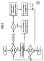
- the memory cells of the integrated memory checked one after the other. For testing the address corresponding to the subsequent memory cell elevated. Every time you start testing a new one Row line, a counter X is set to zero. Becomes a Detected defective, the counter X is increased by one and it is done a comparison of the state of the counter X with one Limit value Y. The limit value Y applies to the number of maximum approved, for repair in the current row line programmed column lines. Checking the memory cells takes place line by line, while when detecting of a defect, the repair was carried out in columns becomes.
- the counter X detects a defect Limit Y does not exceed, the defect is caused by a redundant column line fixed. If the counter exceeds X however the limit Y, the programming of those redundant column lines canceled for repair programmed from defects detected in the current line have been. Then the current row line repaired by a redundant row line.
- the replacing redundant row line checked for errors after replacement becomes.
- the first sub-procedure with the Checking that memory cell of the redundant row line that has the lowest column address. If errors are discovered on the redundant row line, as before, first a repair over the redundant Column lines. Their number exceeds the permitted Limit, their programming is canceled and the redundant row line through another redundant row line replaced. Checking the memory cells of one programmed redundant row line can of course omitted if the redundant lines before programming have been checked and then only error-free redundant lines used for a repair become.
- FIG. 12 there is a memory cell array in the left part of the integrated memory and in the right part an overview of the redundant lines is shown.
- Figures 12 and 13 and 5 to 11 use essentially the same presentation, which is why only once is received.
- the memory cells MC of the integrated Memory are at intersections of bit lines BL and BL Word lines WL arranged.
- the bit lines BL are from 0 to 3 and the word lines WL numbered from 0 to 4.
- Defective memory cells MC are marked by crosses. Already memory cells MC repaired by redundant lines marked by squares.
- a circle marks the current one, that is, a defect in one of the memory cells has just been found MC.
- a table is shown in the right part of FIG. which are all available for illustration contains redundant lines of memory.
- the memory has two redundant word lines RWL0, RWL1 and three redundant bit lines RBL0, RBL1, RBL2. The table indicates which of these redundant lines is already connected to the Replace one of the normal lines BL, WL programmed has been. A zero means that the associated redundant Line has not yet been programmed, and one One means that programming has already taken place.
- FIG. 12 The left part of FIG. 12 also shows which The defective memory cells MC have been repaired are.
- To the right of the memory cell array are those for Replace the respective normal bit lines BL programmed redundant bit lines RBLi entered and below of the memory cell array to replace the normal word lines programmed redundant word lines RWLi. in the The present case took place before that shown in FIG. 12
- State of sequential checking of the memory cells MC starting with the memory cell address 0.0 (i.e. Word line WL0 and bit line BL0), in the direction of Word lines WL.
- the memory cell 0.0 has no defect on.
- the memory cell 0.1 was then checked (word line WL0, bit line BL1), whereby a defect is found has been. This defect was repaired by the bit line 1 was replaced by the redundant bit line RBL0.
- the memory cells were then further tested, whereby at the beginning of the next word line WL1 the error counter X has been reset to 0.
- the defective memory cell 1.0 on the word line WL1 was through the redundant bit line RBL1 repaired and the error counter X increased to the value 1. Since the bit line BL1 is already through the redundant bit line RBL0 has been replaced is the next error found the one with the address 1,2. This is with the redundant Bit line RBL2 repaired.
- the error counter X is set to 2 elevated.
- the defect of the memory cell becomes 1.3 detected. This state is shown in Figure 12. This defect is not repaired with a redundant bit line, since the error counter X is increased to three and thus exceeded the limit value Y, which also has the value two Has.
- Figure 13 shows this state of the integrated memory.
- the Limit value Y is again set to the value 2, since again two of the redundant bit lines RBLi for programming be available. These are the redundant bit lines RBL1 and RBL2, their programming, as just described, has been lifted.
- the memory cells are continuously checked, so that the defect with the next Address 3.0 is determined. This is in turn with a of the redundant bit lines RBLi repaired.
- the first sub-procedure continues in an analogous manner, with programming then some of the redundant bit lines is canceled when the level of counter X exceeds limit value Y exceeds.
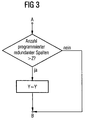
- FIG. 3 is an addition to the flow diagram of FIG. 2 can be seen at the point labeled A and B, after which the limit value Y is then adjusted, for example, if the number of redundant column lines already programmed exceeds a value Z. In this case it says only a relatively small number of redundant column lines available for programming so that the Limit value Y must be reduced to a value Y '.
- the first sub-procedure A1 is ended when all of the defects Memory cells MC are repaired or if after finding Another defect when the limit Y is exceeded all redundant row lines RWL already programmed are.
- Figure 4 shows the flow diagram for one embodiment of the second sub-procedure A2.
- the memory cells are starting checked sequentially with an address ADR. So long no If an error is found, the address is incremented continuously. When the last address has been reached and If there is no defect that cannot be repaired, the integrated one applies Circuit as repaired and the repair procedure will be terminated. As soon as a defective memory cell is found has been carried out as long as there is still a redundant line for programming is available, repair of the Defect by replacing the affected line or the affected column line by a corresponding redundant Management. However, all redundant lines are already programmed, the programming becomes one of the redundant Lines removed so that the original, normal column or row line addressed becomes. Then all memory cells, starting with the start address ADR, checked sequentially again.
- the integrated memory has two redundant word lines RWL0, RWL1 and two redundant bit lines RBL0, RBL1.
- Defective memory cells MC are in turn by crosses Marked memory cell array. The circle marks the current defect found.
- the repair of detected defects is done in this embodiment by programming of the redundant lines in the in the table in right part of the figures shown order. For repairs of the first defect with address 0.1 (word line WL0, Bit line BL1) therefore becomes the redundant word line RWL0 used.
- a pointer P points to the next one redundant line using.
- Figure 6 shows the integrated memory after the word line WL0 address-wise through the redundant word line RBL0 has been replaced.
- the programming of the redundant Word line RWL0 is identified by a 1 in the table.
- the pointer P points to the one to be programmed next redundant line RWL1.
- Checking the memory cells is continued sequentially and next the defect the memory cell 1.0 determined. According to Figure 7 this is Defect due to programming of the redundant word line RWL1 repaired.
- the other defects are also automatic repaired on the word line WL1 without this being checked Need to become. This assumes that the programmed redundant lines are error-free. This can be done by performing a test before programming be determined. Only those that are found to be error-free detected redundant lines used for a repair.
- next defect found is the one with the address 3.0.
- the pointer P now points to the third redundant Line RBL0, so that the current defect by the redundant Bit line RBL0 is replaced. This is shown in Figure 8. According to Figure 9, the next defect with the address 3.1 replaced by the redundant bit line RBL1.
- the Pointer P advances to the next redundant line.
- the Memory test is carried out with the memory cells that have not yet been tested MC continues and the defect with address 4.2 is determined. Then the programming of the redundant Word line RWL1, to which pointer P points, has been undone.
- the memory cells are starting with the address 0.0 checked again, the defect with the address 1.2 as first is determined. Its address is smaller than that Address 4.2 of the current defect. Hence the repeal programming the redundant word line RWL1 again reversed.
- the pointer advances to the next redundant line RBL0 ( Figure 11). Because the current defect with the address 4.2 still is not always repaired, now programming this redundant line RBL0 canceled.
- the memory cells are tested again starting with the start address 0.0. Here no defect is found before the current defect with the address 4.2. This is because the defects with the addresses 1.0 and 3.0 already by the redundant Word lines RBL1 and RWL0 have been repaired. Consequently the redundant bit line RBL0 that has become free can be used Repair of the current defect can be programmed. This State is shown in Figure 11.
- the pointer P moves to the next programmed redundant line RBL1. Finally the memory cell with the address 4.3 is still checked, that has no defect. Hence the repair procedure completed with a fully repaired built-in memory.
- Figure 1 shows a flow diagram of an embodiment of the invention Repair procedure. This starts with a call of the first sub-method A1, with a start value YS for the limit value Y is set.
- the first sub-procedure A1 ends, as described, when all defective memory cells MC are repaired or if another defect is found if the limit value Y is exceeded, all redundant ones Row lines are already programmed. That means a Cancellation of all programming of redundant column lines RBL due to in the affected row line WL detected defects have occurred, can not take place because the affected line WL is not through one of the redundant Row lines RWL can be replaced.
- an error signature is generated R created in the form of a register.
- the number of memory cells checked MC can, for example, use the address of the last checked Memory cell MC or via the address of the next memory cell MC to be checked.
- the Repair result is expressed in the number of programmed redundant lines RBL, RWL or the number of remaining redundant lines RBL, RWL, here as RRBL, Referred to as RRWL.
- the further procedure is determined. Does this correspond to the last address EA of the memory to be checked are all defective memory cells MC repaired and the procedure is completed.
- the second sub-procedure becomes A2 called, the start value of the address ADR the value of the Receives address AD of the last checked memory cell MC. That is, the second sub-procedure A2 begins with the last checked Memory cell MC, it starts the programming of the previous sub-process A1. The The procedure ends in any case after the end of the second Sub-procedure A2. Can not repair all memory cells MC the memory is marked as defective.
- the information of the error signature R is based on a or several parameters cached. These are during the duration of the procedure changeable. As parameters here the address AD of the memory cell MC last checked, the number of remaining redundant lines RRBL, RRWL and the respective value YS as the initial value for the limit value Y used for a following first sub-process A1.
- sub-process A1 can start with limit value Y. of the procedure can be varied more (will be based on the corresponding Digit increased or decreased by more than 1) and less strong at the end of the process. So you “feel” yourself step by step to a sufficiently good solution (mathematically in other words, when you search for a solution, you get a "global Minimum "and does not end in a” local minimum "). With the second sub-procedure will be carried out as the repair progresses any double repairs canceled.
- A1 and A2 other or further sub-processes are used, which differ in terms of their repair strategy for the described sub-processes A1 and A2 are.
- the strengths of such sub-processes can be found in the search for a solution to other fault patterns.
- the parameters of the error signatures R to the following To submit sub-proceedings. So that can go to the previous Repair result to be tied up.
- the respective error signature R is at the beginning of the following The previous repair result, discarded in whole or in part.
- the error signature with regard to the parameters used adjust accordingly.
Landscapes
- For Increasing The Reliability Of Semiconductor Memories (AREA)
Abstract
Description
Es zeigen:
- Figur 1
- ein Flußdiagramm einer Ausführungsform des Reparaturverfahrens,
- Figur 2
- ein Flußdiagramm einer Ausführungsform des ersten Teilverfahrens,
- Figur 3
- eine Ergänzung des Flußdiagramms aus Figur 2,
- Figur 4
- ein Flußdiagramm einer Ausführungsform des zweiten Teilverfahrens,
- Figur 5 bis 11
- ein Ausführungsbeispiel für die Durchführung des in Figur 4 dargestellten Teilverfahrens und
- Figuren 12 und 13
- ein Ausführungsbeispiel für die Durchführung des in Figur 2 dargestellten Teilverfahrens.
Claims (10)
- Verfahren zur Reparatur von defekten Speicherzellen (MC) eines integrierten Halbleiterspeichers, die an je eine Zeilenleitung (WL) und je eine Spaltenleitung (BL) angeschlossen sind, durch eine reversible Programmierung von redundanten Zeilenleitungen (RWL) und redundanten Spaltenleitungen (RBL) mit folgenden Merkmalen:es werden wenigstens zwei unterschiedliche Teilverfahren (A1, A2) zur Reparatur von defekten Speicherzellen (MC) verwendet, die nacheinander ablaufen,in den Teilverfahren (A1, A2) werden die Speicherzellen (MC) nacheinander geprüft, und jeweils nach dem Feststellen eines Defektes der jeweils geprüften Speicherzelle wird vor dem Überprüfen einer weiteren Speicherzelle die Zeilenleitung (WL) oder die Spaltenleitung (BL), an die die Speicherzelle angeschlossen ist, für die der Defekt festgestellt wurde, durch Programmierung einer der redundanten Leitungen (RWL, RBL) ersetzt,die Teilverfahren (A1, A2) unterscheiden sich in der Reihenfolge der Überprüfung der Speicherzellen (MC) und darin, welche der redundanten Leitungen (RWL, RBL) zum Ersatz der betroffenen Zeilenleitung (WL) oder der betroffenen Spaltenleitung (BL) programmiert wird,es wird ein Teilverfahren (A1, A2) mit einer das Teilverfahren abschließenden Fehlersignatur (R) aufgerufen, die Information über die Anzahl der überprüften Speicherzellen (MC) und die Anzahl der programmierten redundanten Leitungen (RBL, RWL) oder verbleibenden redundanten Leitungen (RRBL, RRWL) enthält,im Anschluß wird abhängig von der Fehlersignatur (R) des vorangegangenen Teilverfahrens (A1, A2) ein anderes der Teilverfahren (A1, A2) aufgerufen, das zu Beginn die vorgenommene Programmierung nicht, teilweise oder ganz aufhebt.
- Verfahren nach Anspruch 1,
dadurch gekennzeichnet, daß das Verfahren solange mit dem Aufruf eines der Teilverfahren (A1, A2) fortgesetzt wird, bis alle Speicherzellen (MC) überprüft und repariert sind oder der Speicher als nicht reparierbar gekennzeichnet ist. - Verfahren nach einem der vorhergehenden Ansprüche,
dadurch gekennzeichnet, daß die Fehlersignatur (R) ein oder mehrere Parameter (AD, RRWL, RRBL, YS) umfaßt, die während der Laufzeit in ihren Werten veränderbar sind. - Verfahren nach Anspruch 3,
dadurch gekennzeichnet, daß die Werte der veränderbaren Parameter (AD, RRWL, RRBL, YS) jeweils an das dem gerade aktiven Teilverfahren (A1, A2) folgende Teilverfahren (A1, A2) übergeben werden. - Verfahren nach einem der vorhergehenden Ansprüche,
dadurch gekennzeichnet, daß die Teilverfahren (A1, A2) folgende Schritte umfassen:nach erfolgter Programmierung einer bestimmten Anzahl der redundanten Leitungen (RWL, RBL) wird bei Feststellen eines weiteren Defektes die Programmierung wenigstens einer der redundanten Leitungen aufgehoben,und diese redundante Leitung (RWL, RBL) wird zur Reparatur eines Defektes einer anderen Speicherzelle (MC) programmiert. - Verfahren nach Anspruch 5,
dadurch gekennzeichnet, daß ein erstes Teilverfahren (A1) folgende Schritte umfaßt:in vorangegangenen Teilverfahren (A1, A2) vorgenommene Programmierungen von redundanten Leitungen (RWL, RBL) werden aufgehoben,die Speicherzellen (MC) werden, beginnend mit einer Startadresse, zeilenweise auf Defekte geprüft,bei Feststellen eines Defektes der gerade geprüften Speicherzelle (MC) wird die betroffene Spaltenleitung (BL) durch eine der redundanten Spaltenleitungen (RBL) ersetzt, sofern die Anzahl (X) der programmierten redundanten Spaltenleitungen RBL dabei einen Grenzwert (Y) nicht überschreitet,bei Überschreiten des Grenzwertes (Y) werden alle Programmierungen von redundanten Spaltenleitungen (RBL), die aufgrund von in der betroffenen Zeilenleitung (WL) festgestellten Defekten erfolgt sind, aufgehoben,und die betroffene Zeilenleitung (WL) wird durch eine der redundanten Zeilenleitungen (RWL) ersetzt. - Verfahren nach Anspruch 6,
dadurch gekennzeichnet, daß das erste Teilverfahren (A1) beendet wird, wenn alle Speicherzellen (MC) repariert sind oder wenn nach Feststellen des weiteren Defektes bei Überschreiten des Grenzwertes (Y) alle redundanten Zeilenleitungen (RWL) bereits programmiert sind. - Verfahren nach Anspruch 6,
dadurch gekennzeichnet, daß der Grenzwert (Y) während der Laufzeit des ersten Teilverfahrens (A1) verändert wird. - Verfahren nach Anspruch 5,
dadurch gekennzeichnet, daß ein zweites Teilverfahren (A2) folgende Schritte umfaßt:die Speicherzellen (MC) werden, beginnend mit einer Startadresse, geprüft,nachdem alle redundanten Leitungen (RWL, RBL) programmiert worden sind, wird bei Feststellen eines weiteren Defektes die Programmierung einer der redundanten Leitungen aufgehoben,die Speicherzellen (MC) werden anschließend, beginnend mit der Startadresse, erneut geprüft,sofern dabei ein Defekt festgestellt wird, der adressenmäßig vor dem weiteren Defekt angeordnet ist, wird die Aufhebung der Programmierung der entsprechenden redundanten Leitung (RWL, RBL) rückgängig gemacht,anschließend werden die drei vorhergehenden Verfahrensschritte bezüglich der Aufhebung der Programmierung einer anderen der redundanten Leitungen (RWL, RBL) wiederholt,sofern nach der Aufhebung der Programmierung einer der redundanten Leitungen (RWL, RBL) während des daran anschließenden Prüfens der Speicherzellen (MC) kein Defekt festgestellt wird, der adressenmäßig vor dem weiteren Defekt angeordnet ist, wird dieser mit der durch die Aufhebung ihrer Programmierung frei gewordenen redundanten Leitung repariert. - Verfahren nach Anspruch 9,
dadurch gekennzeichnet, daß das zweite Teilverfahren (A2) beendet wird, wenn alle Speicherzellen (MC) repariert sind oder wenn nach Feststellen des weiteren Defektes die nacheinander durchgeführte Aufhebung der Programmierung aller redundanten Leitungen (RBL, RWL) keine Reparatur aller bislang erkannten Defekte ermöglicht.
Applications Claiming Priority (2)
| Application Number | Priority Date | Filing Date | Title |
|---|---|---|---|
| DE19901206A DE19901206C2 (de) | 1999-01-14 | 1999-01-14 | Verfahren zur Reparatur von defekten Speicherzellen eines integrierten Halbleiterspeichers |
| DE19901206 | 1999-01-14 |
Publications (2)
| Publication Number | Publication Date |
|---|---|
| EP1020795A1 true EP1020795A1 (de) | 2000-07-19 |
| EP1020795B1 EP1020795B1 (de) | 2003-05-14 |
Family
ID=7894248
Family Applications (1)
| Application Number | Title | Priority Date | Filing Date |
|---|---|---|---|
| EP00100222A Expired - Lifetime EP1020795B1 (de) | 1999-01-14 | 2000-01-14 | Verfahren zur Reparatur von defekten Speicherzellen eines integrierten Halbleiterspeichers |
Country Status (3)
| Country | Link |
|---|---|
| US (1) | US6292414B1 (de) |
| EP (1) | EP1020795B1 (de) |
| DE (2) | DE19901206C2 (de) |
Families Citing this family (1)
| Publication number | Priority date | Publication date | Assignee | Title |
|---|---|---|---|---|
| TW200921691A (en) * | 2007-11-14 | 2009-05-16 | Etron Technology Inc | Method for controlling a dram |
Citations (2)
| Publication number | Priority date | Publication date | Assignee | Title |
|---|---|---|---|---|
| EP0140595A2 (de) * | 1983-10-06 | 1985-05-08 | Eaton Corporation | Hochgeschwindigkeitsredundanzprozessor |
| DE19736250A1 (de) * | 1996-08-20 | 1998-02-26 | Advantest Corp | Fehlerreparaturverfahren für ein Speicherbauelement |
Family Cites Families (9)
| Publication number | Priority date | Publication date | Assignee | Title |
|---|---|---|---|---|
| ATE87753T1 (de) * | 1988-02-10 | 1993-04-15 | Siemens Ag | Redundanzdekoder eines integrierten halbleiterspeichers. |
| JP2842923B2 (ja) * | 1990-03-19 | 1999-01-06 | 株式会社アドバンテスト | 半導体メモリ試験装置 |
| US5206583A (en) * | 1991-08-20 | 1993-04-27 | International Business Machines Corporation | Latch assisted fuse testing for customized integrated circuits |
| US5550394A (en) * | 1993-06-18 | 1996-08-27 | Texas Instruments Incorporated | Semiconductor memory device and defective memory cell correction circuit |
| US5519657A (en) * | 1993-09-30 | 1996-05-21 | Mitsubishi Denki Kabushiki Kaisha | Semiconductor memory device having a redundant memory array and a testing method thereof |
| JP3774500B2 (ja) * | 1995-05-12 | 2006-05-17 | 株式会社ルネサステクノロジ | 半導体記憶装置 |
| US6021512A (en) * | 1996-11-27 | 2000-02-01 | International Business Machines Corporation | Data processing system having memory sub-array redundancy and method therefor |
| US5920515A (en) * | 1997-09-26 | 1999-07-06 | Advanced Micro Devices, Inc. | Register-based redundancy circuit and method for built-in self-repair in a semiconductor memory device |
| DE19838861A1 (de) | 1998-08-26 | 2000-03-02 | Siemens Ag | Verfahren zur Reparatur von defekten Speicherzellen eines integrierten Speichers |
-
1999
- 1999-01-14 DE DE19901206A patent/DE19901206C2/de not_active Expired - Fee Related
-
2000
- 2000-01-14 US US09/483,738 patent/US6292414B1/en not_active Expired - Lifetime
- 2000-01-14 DE DE50002130T patent/DE50002130D1/de not_active Expired - Fee Related
- 2000-01-14 EP EP00100222A patent/EP1020795B1/de not_active Expired - Lifetime
Patent Citations (2)
| Publication number | Priority date | Publication date | Assignee | Title |
|---|---|---|---|---|
| EP0140595A2 (de) * | 1983-10-06 | 1985-05-08 | Eaton Corporation | Hochgeschwindigkeitsredundanzprozessor |
| DE19736250A1 (de) * | 1996-08-20 | 1998-02-26 | Advantest Corp | Fehlerreparaturverfahren für ein Speicherbauelement |
Non-Patent Citations (2)
| Title |
|---|
| DAY J R: "A FAULT-DRIVEN, COMPREHENSIVE REDUNDANCY ALGORITHM", IEEE DESIGN & TEST OF COMPUTERS,US,IEEE COMPUTERS SOCIETY. LOS ALAMITOS, vol. 2, no. 3, 1 June 1985 (1985-06-01), pages 35 - 44, XP000744056, ISSN: 0740-7475 * |
| LOMBARDI F ET AL: "APPROACHES FOR THE REPAIR OF VLSI/WSI BRAMS BY ROW/COLUMN DELETION", INTERNATIONAL SYMPOSIUM ON FAULT TOLERANT COMPUTING SYSTEMS. (FTCS),US,WASHINGTON, IEEE COMP. SOC. PRESS, vol. SYMP. 18, 1988, pages 342 - 347, XP000619023 * |
Also Published As
| Publication number | Publication date |
|---|---|
| DE19901206C2 (de) | 2003-02-06 |
| EP1020795B1 (de) | 2003-05-14 |
| DE19901206A1 (de) | 2000-07-27 |
| US6292414B1 (en) | 2001-09-18 |
| DE50002130D1 (de) | 2003-06-18 |
Similar Documents
| Publication | Publication Date | Title |
|---|---|---|
| EP1105802B1 (de) | Verfahren zur reparatur von defekten speicherzellen eines integrierten speichers | |
| EP1444699B1 (de) | Verfahren zur rekonfiguration eines speichers | |
| EP1008993B1 (de) | Schreib/Lesespeicher mit Selbsttestvorrichtung und zugehöriges Testverfahren | |
| DE10225381A1 (de) | Verfahren und Vorrichtung zum Speichern von Speichertestinformantion | |
| EP1124232A2 (de) | Integrierter Halbleiterspeicher mit redundanter Einheit von Speicherzellen | |
| EP1113362B1 (de) | Integrierter Halbleiterspeicher mit einer Speichereinheit zum Speichern von Adressen fehlerhafter Speicherzellen | |
| DE60311117T2 (de) | Verfahren und schaltkreise zum identifizieren schwacher bit in einem mram | |
| DE1906940C3 (de) | ||
| DE10206689B4 (de) | Integrierter Speicher und Verfahren zum Betrieb eines integrierten Speichers | |
| DE1906940B2 (de) | Wortorganisierter speicher mit redundanten wortplaetzen | |
| DE10337284A1 (de) | Integrierter Speicher mit einer Schaltung zum Funktionstest des integrierten Speichers sowie Verfahren zum Betrieb des integrierten Speichers | |
| DE19922786B4 (de) | Halbleiterspeicher mit Testeinrichtung | |
| EP0902924B1 (de) | Redundanzspeichervorrichtung mit rom-speicherzellen | |
| EP0615211A1 (de) | Verfahren zum Speichern sicherheitsrelevanter Daten | |
| DE69323076T2 (de) | Verfahren zur Erkennung fehlerhafter Elemente eines redundanten Halbleiterspeichers | |
| DE19725581C2 (de) | Verfahren zur Funktionsüberprüfung von Speicherzellen eines integrierten Speichers | |
| DE19904375C2 (de) | Verfahren zur Funktionsüberprüfung von Speicherzellen eines integrierten Halbleiterspeichers | |
| EP1020795B1 (de) | Verfahren zur Reparatur von defekten Speicherzellen eines integrierten Halbleiterspeichers | |
| DE10331068A1 (de) | Verfahren zum Auslesen von Fehlerinformationen aus einem integrierten Baustein und integrierter Speicherbaustein | |
| DE10016719A1 (de) | Integrierter Speicher und Verfahren zur Funktionsprüfung von Speicherzellen eines integrierten Speichers | |
| DE10062404A1 (de) | Vorrichtung und Verfahren zum Reduzieren der Anzahl von Adressen fehlerhafter Speicherzellen | |
| EP1141834B1 (de) | Integrierter speicher mit redundanz | |
| EP0353660A2 (de) | Verfahren zur Fehlersicherung in Speichersystemen von Datenverarbeitungsanlagen, insbesondere Fernsprechvermittlungsanlagen | |
| DE10341555B4 (de) | Topographiekorrektur zum Testen redundanter Arrayelemente | |
| DE10224729A1 (de) | Vorrichtung zum Testen einer Halbleitervorrichtung |
Legal Events
| Date | Code | Title | Description |
|---|---|---|---|
| PUAI | Public reference made under article 153(3) epc to a published international application that has entered the european phase |
Free format text: ORIGINAL CODE: 0009012 |
|
| AK | Designated contracting states |
Kind code of ref document: A1 Designated state(s): DE FR GB IE IT |
|
| AX | Request for extension of the european patent |
Free format text: AL;LT;LV;MK;RO;SI |
|
| 17P | Request for examination filed |
Effective date: 20000818 |
|
| AKX | Designation fees paid | ||
| RBV | Designated contracting states (corrected) |
Designated state(s): DE FR GB IE IT |
|
| GRAG | Despatch of communication of intention to grant |
Free format text: ORIGINAL CODE: EPIDOS AGRA |
|
| 17Q | First examination report despatched |
Effective date: 20020507 |
|
| GRAG | Despatch of communication of intention to grant |
Free format text: ORIGINAL CODE: EPIDOS AGRA |
|
| GRAH | Despatch of communication of intention to grant a patent |
Free format text: ORIGINAL CODE: EPIDOS IGRA |
|
| GRAH | Despatch of communication of intention to grant a patent |
Free format text: ORIGINAL CODE: EPIDOS IGRA |
|
| GRAA | (expected) grant |
Free format text: ORIGINAL CODE: 0009210 |
|
| AK | Designated contracting states |
Designated state(s): DE FR GB IE IT |
|
| PG25 | Lapsed in a contracting state [announced via postgrant information from national office to epo] |
Ref country code: IT Free format text: LAPSE BECAUSE OF FAILURE TO SUBMIT A TRANSLATION OF THE DESCRIPTION OR TO PAY THE FEE WITHIN THE PRE;WARNING: LAPSES OF ITALIAN PATENTS WITH EFFECTIVE DATE BEFORE 2007 MAY HAVE OCCURRED AT ANY TIME BEFORE 2007. THE CORRECT EFFECTIVE DATE MAY BE DIFFERENT FROM THE ONE RECORDED.SCRIBED TIME-LIMIT Effective date: 20030514 Ref country code: FR Free format text: LAPSE BECAUSE OF FAILURE TO SUBMIT A TRANSLATION OF THE DESCRIPTION OR TO PAY THE FEE WITHIN THE PRESCRIBED TIME-LIMIT Effective date: 20030514 |
|
| REG | Reference to a national code |
Ref country code: GB Ref legal event code: FG4D Free format text: NOT ENGLISH |
|
| REG | Reference to a national code |
Ref country code: IE Ref legal event code: FG4D Free format text: GERMAN |
|
| REF | Corresponds to: |
Ref document number: 50002130 Country of ref document: DE Date of ref document: 20030618 Kind code of ref document: P |
|
| GBT | Gb: translation of ep patent filed (gb section 77(6)(a)/1977) | ||
| PLBE | No opposition filed within time limit |
Free format text: ORIGINAL CODE: 0009261 |
|
| STAA | Information on the status of an ep patent application or granted ep patent |
Free format text: STATUS: NO OPPOSITION FILED WITHIN TIME LIMIT |
|
| 26N | No opposition filed |
Effective date: 20040217 |
|
| EN | Fr: translation not filed | ||
| PGFP | Annual fee paid to national office [announced via postgrant information from national office to epo] |
Ref country code: GB Payment date: 20070119 Year of fee payment: 8 |
|
| PGFP | Annual fee paid to national office [announced via postgrant information from national office to epo] |
Ref country code: IE Payment date: 20080122 Year of fee payment: 9 |
|
| PGFP | Annual fee paid to national office [announced via postgrant information from national office to epo] |
Ref country code: DE Payment date: 20080315 Year of fee payment: 9 |
|
| GBPC | Gb: european patent ceased through non-payment of renewal fee |
Effective date: 20080114 |
|
| PG25 | Lapsed in a contracting state [announced via postgrant information from national office to epo] |
Ref country code: GB Free format text: LAPSE BECAUSE OF NON-PAYMENT OF DUE FEES Effective date: 20080114 |
|
| REG | Reference to a national code |
Ref country code: IE Ref legal event code: MM4A |
|
| PG25 | Lapsed in a contracting state [announced via postgrant information from national office to epo] |
Ref country code: DE Free format text: LAPSE BECAUSE OF NON-PAYMENT OF DUE FEES Effective date: 20090801 |
|
| PG25 | Lapsed in a contracting state [announced via postgrant information from national office to epo] |
Ref country code: IE Free format text: LAPSE BECAUSE OF NON-PAYMENT OF DUE FEES Effective date: 20090114 |