EP1018760A1 - Procédé et dispositif pour encapsuler un dispositif électronique, spécialement une puce semi-conductrice - Google Patents
Procédé et dispositif pour encapsuler un dispositif électronique, spécialement une puce semi-conductrice Download PDFInfo
- Publication number
- EP1018760A1 EP1018760A1 EP99810009A EP99810009A EP1018760A1 EP 1018760 A1 EP1018760 A1 EP 1018760A1 EP 99810009 A EP99810009 A EP 99810009A EP 99810009 A EP99810009 A EP 99810009A EP 1018760 A1 EP1018760 A1 EP 1018760A1
- Authority
- EP
- European Patent Office
- Prior art keywords
- dispenser
- component
- carrier
- station
- adhesive
- Prior art date
- Legal status (The legal status is an assumption and is not a legal conclusion. Google has not performed a legal analysis and makes no representation as to the accuracy of the status listed.)
- Withdrawn
Links
- 238000000034 method Methods 0.000 title claims abstract description 37
- 239000004065 semiconductor Substances 0.000 title claims abstract description 10
- 239000000872 buffer Substances 0.000 claims abstract description 55
- 239000000853 adhesive Substances 0.000 claims abstract description 37
- 230000001070 adhesive effect Effects 0.000 claims abstract description 37
- 239000000463 material Substances 0.000 claims abstract description 24
- 238000007639 printing Methods 0.000 claims abstract description 8
- 239000007788 liquid Substances 0.000 claims abstract description 4
- 239000004020 conductor Substances 0.000 claims description 9
- 230000001681 protective effect Effects 0.000 claims description 8
- 150000001875 compounds Chemical class 0.000 claims description 7
- 239000003795 chemical substances by application Substances 0.000 claims description 3
- 238000010438 heat treatment Methods 0.000 claims description 3
- 235000011837 pasties Nutrition 0.000 claims description 3
- 230000005670 electromagnetic radiation Effects 0.000 claims description 2
- 239000003292 glue Substances 0.000 claims 1
- 238000004519 manufacturing process Methods 0.000 description 9
- 238000005538 encapsulation Methods 0.000 description 5
- 239000010410 layer Substances 0.000 description 5
- 239000012790 adhesive layer Substances 0.000 description 3
- 230000008901 benefit Effects 0.000 description 3
- 238000006073 displacement reaction Methods 0.000 description 3
- 229920002379 silicone rubber Polymers 0.000 description 3
- 229910000679 solder Inorganic materials 0.000 description 3
- XUIMIQQOPSSXEZ-UHFFFAOYSA-N Silicon Chemical compound [Si] XUIMIQQOPSSXEZ-UHFFFAOYSA-N 0.000 description 2
- 238000005516 engineering process Methods 0.000 description 2
- 239000004033 plastic Substances 0.000 description 2
- 229910052710 silicon Inorganic materials 0.000 description 2
- 239000010703 silicon Substances 0.000 description 2
- 238000004026 adhesive bonding Methods 0.000 description 1
- 238000004378 air conditioning Methods 0.000 description 1
- 230000009286 beneficial effect Effects 0.000 description 1
- 230000015572 biosynthetic process Effects 0.000 description 1
- 239000007795 chemical reaction product Substances 0.000 description 1
- 238000000151 deposition Methods 0.000 description 1
- 238000001035 drying Methods 0.000 description 1
- 229920001721 polyimide Polymers 0.000 description 1
- 238000003825 pressing Methods 0.000 description 1
- 238000000926 separation method Methods 0.000 description 1
- 125000006850 spacer group Chemical group 0.000 description 1
- 238000001228 spectrum Methods 0.000 description 1
- 239000002759 woven fabric Substances 0.000 description 1
Images


Classifications
-
- H—ELECTRICITY
- H01—ELECTRIC ELEMENTS
- H01L—SEMICONDUCTOR DEVICES NOT COVERED BY CLASS H10
- H01L21/00—Processes or apparatus adapted for the manufacture or treatment of semiconductor or solid state devices or of parts thereof
- H01L21/67—Apparatus specially adapted for handling semiconductor or electric solid state devices during manufacture or treatment thereof; Apparatus specially adapted for handling wafers during manufacture or treatment of semiconductor or electric solid state devices or components ; Apparatus not specifically provided for elsewhere
- H01L21/67005—Apparatus not specifically provided for elsewhere
- H01L21/67011—Apparatus for manufacture or treatment
- H01L21/67132—Apparatus for placing on an insulating substrate, e.g. tape
-
- H—ELECTRICITY
- H01—ELECTRIC ELEMENTS
- H01L—SEMICONDUCTOR DEVICES NOT COVERED BY CLASS H10
- H01L21/00—Processes or apparatus adapted for the manufacture or treatment of semiconductor or solid state devices or of parts thereof
- H01L21/02—Manufacture or treatment of semiconductor devices or of parts thereof
- H01L21/04—Manufacture or treatment of semiconductor devices or of parts thereof the devices having potential barriers, e.g. a PN junction, depletion layer or carrier concentration layer
- H01L21/50—Assembly of semiconductor devices using processes or apparatus not provided for in a single one of the subgroups H01L21/06 - H01L21/326, e.g. sealing of a cap to a base of a container
- H01L21/56—Encapsulations, e.g. encapsulation layers, coatings
- H01L21/563—Encapsulation of active face of flip-chip device, e.g. underfilling or underencapsulation of flip-chip, encapsulation preform on chip or mounting substrate
-
- H—ELECTRICITY
- H01—ELECTRIC ELEMENTS
- H01L—SEMICONDUCTOR DEVICES NOT COVERED BY CLASS H10
- H01L21/00—Processes or apparatus adapted for the manufacture or treatment of semiconductor or solid state devices or of parts thereof
- H01L21/67—Apparatus specially adapted for handling semiconductor or electric solid state devices during manufacture or treatment thereof; Apparatus specially adapted for handling wafers during manufacture or treatment of semiconductor or electric solid state devices or components ; Apparatus not specifically provided for elsewhere
- H01L21/67005—Apparatus not specifically provided for elsewhere
- H01L21/67011—Apparatus for manufacture or treatment
- H01L21/67126—Apparatus for sealing, encapsulating, glassing, decapsulating or the like
-
- H—ELECTRICITY
- H01—ELECTRIC ELEMENTS
- H01L—SEMICONDUCTOR DEVICES NOT COVERED BY CLASS H10
- H01L23/00—Details of semiconductor or other solid state devices
- H01L23/28—Encapsulations, e.g. encapsulating layers, coatings, e.g. for protection
- H01L23/31—Encapsulations, e.g. encapsulating layers, coatings, e.g. for protection characterised by the arrangement or shape
- H01L23/3107—Encapsulations, e.g. encapsulating layers, coatings, e.g. for protection characterised by the arrangement or shape the device being completely enclosed
- H01L23/3114—Encapsulations, e.g. encapsulating layers, coatings, e.g. for protection characterised by the arrangement or shape the device being completely enclosed the device being a chip scale package, e.g. CSP
-
- H—ELECTRICITY
- H01—ELECTRIC ELEMENTS
- H01L—SEMICONDUCTOR DEVICES NOT COVERED BY CLASS H10
- H01L24/00—Arrangements for connecting or disconnecting semiconductor or solid-state bodies; Methods or apparatus related thereto
- H01L24/01—Means for bonding being attached to, or being formed on, the surface to be connected, e.g. chip-to-package, die-attach, "first-level" interconnects; Manufacturing methods related thereto
- H01L24/26—Layer connectors, e.g. plate connectors, solder or adhesive layers; Manufacturing methods related thereto
- H01L24/28—Structure, shape, material or disposition of the layer connectors prior to the connecting process
-
- H—ELECTRICITY
- H01—ELECTRIC ELEMENTS
- H01L—SEMICONDUCTOR DEVICES NOT COVERED BY CLASS H10
- H01L24/00—Arrangements for connecting or disconnecting semiconductor or solid-state bodies; Methods or apparatus related thereto
- H01L24/80—Methods for connecting semiconductor or other solid state bodies using means for bonding being attached to, or being formed on, the surface to be connected
- H01L24/83—Methods for connecting semiconductor or other solid state bodies using means for bonding being attached to, or being formed on, the surface to be connected using a layer connector
-
- H—ELECTRICITY
- H01—ELECTRIC ELEMENTS
- H01L—SEMICONDUCTOR DEVICES NOT COVERED BY CLASS H10
- H01L2224/00—Indexing scheme for arrangements for connecting or disconnecting semiconductor or solid-state bodies and methods related thereto as covered by H01L24/00
- H01L2224/01—Means for bonding being attached to, or being formed on, the surface to be connected, e.g. chip-to-package, die-attach, "first-level" interconnects; Manufacturing methods related thereto
- H01L2224/26—Layer connectors, e.g. plate connectors, solder or adhesive layers; Manufacturing methods related thereto
- H01L2224/31—Structure, shape, material or disposition of the layer connectors after the connecting process
- H01L2224/32—Structure, shape, material or disposition of the layer connectors after the connecting process of an individual layer connector
- H01L2224/321—Disposition
- H01L2224/32151—Disposition the layer connector connecting between a semiconductor or solid-state body and an item not being a semiconductor or solid-state body, e.g. chip-to-substrate, chip-to-passive
- H01L2224/32221—Disposition the layer connector connecting between a semiconductor or solid-state body and an item not being a semiconductor or solid-state body, e.g. chip-to-substrate, chip-to-passive the body and the item being stacked
- H01L2224/32225—Disposition the layer connector connecting between a semiconductor or solid-state body and an item not being a semiconductor or solid-state body, e.g. chip-to-substrate, chip-to-passive the body and the item being stacked the item being non-metallic, e.g. insulating substrate with or without metallisation
-
- H—ELECTRICITY
- H01—ELECTRIC ELEMENTS
- H01L—SEMICONDUCTOR DEVICES NOT COVERED BY CLASS H10
- H01L2224/00—Indexing scheme for arrangements for connecting or disconnecting semiconductor or solid-state bodies and methods related thereto as covered by H01L24/00
- H01L2224/01—Means for bonding being attached to, or being formed on, the surface to be connected, e.g. chip-to-package, die-attach, "first-level" interconnects; Manufacturing methods related thereto
- H01L2224/50—Tape automated bonding [TAB] connectors, i.e. film carriers; Manufacturing methods related thereto
-
- H—ELECTRICITY
- H01—ELECTRIC ELEMENTS
- H01L—SEMICONDUCTOR DEVICES NOT COVERED BY CLASS H10
- H01L2224/00—Indexing scheme for arrangements for connecting or disconnecting semiconductor or solid-state bodies and methods related thereto as covered by H01L24/00
- H01L2224/73—Means for bonding being of different types provided for in two or more of groups H01L2224/10, H01L2224/18, H01L2224/26, H01L2224/34, H01L2224/42, H01L2224/50, H01L2224/63, H01L2224/71
- H01L2224/732—Location after the connecting process
- H01L2224/73201—Location after the connecting process on the same surface
- H01L2224/73203—Bump and layer connectors
-
- H—ELECTRICITY
- H01—ELECTRIC ELEMENTS
- H01L—SEMICONDUCTOR DEVICES NOT COVERED BY CLASS H10
- H01L2224/00—Indexing scheme for arrangements for connecting or disconnecting semiconductor or solid-state bodies and methods related thereto as covered by H01L24/00
- H01L2224/80—Methods for connecting semiconductor or other solid state bodies using means for bonding being attached to, or being formed on, the surface to be connected
- H01L2224/83—Methods for connecting semiconductor or other solid state bodies using means for bonding being attached to, or being formed on, the surface to be connected using a layer connector
- H01L2224/831—Methods for connecting semiconductor or other solid state bodies using means for bonding being attached to, or being formed on, the surface to be connected using a layer connector the layer connector being supplied to the parts to be connected in the bonding apparatus
- H01L2224/83102—Methods for connecting semiconductor or other solid state bodies using means for bonding being attached to, or being formed on, the surface to be connected using a layer connector the layer connector being supplied to the parts to be connected in the bonding apparatus using surface energy, e.g. capillary forces
-
- H—ELECTRICITY
- H01—ELECTRIC ELEMENTS
- H01L—SEMICONDUCTOR DEVICES NOT COVERED BY CLASS H10
- H01L2224/00—Indexing scheme for arrangements for connecting or disconnecting semiconductor or solid-state bodies and methods related thereto as covered by H01L24/00
- H01L2224/80—Methods for connecting semiconductor or other solid state bodies using means for bonding being attached to, or being formed on, the surface to be connected
- H01L2224/83—Methods for connecting semiconductor or other solid state bodies using means for bonding being attached to, or being formed on, the surface to be connected using a layer connector
- H01L2224/8312—Aligning
- H01L2224/83136—Aligning involving guiding structures, e.g. spacers or supporting members
-
- H—ELECTRICITY
- H01—ELECTRIC ELEMENTS
- H01L—SEMICONDUCTOR DEVICES NOT COVERED BY CLASS H10
- H01L2224/00—Indexing scheme for arrangements for connecting or disconnecting semiconductor or solid-state bodies and methods related thereto as covered by H01L24/00
- H01L2224/80—Methods for connecting semiconductor or other solid state bodies using means for bonding being attached to, or being formed on, the surface to be connected
- H01L2224/83—Methods for connecting semiconductor or other solid state bodies using means for bonding being attached to, or being formed on, the surface to be connected using a layer connector
- H01L2224/8319—Arrangement of the layer connectors prior to mounting
- H01L2224/83192—Arrangement of the layer connectors prior to mounting wherein the layer connectors are disposed only on another item or body to be connected to the semiconductor or solid-state body
-
- H—ELECTRICITY
- H01—ELECTRIC ELEMENTS
- H01L—SEMICONDUCTOR DEVICES NOT COVERED BY CLASS H10
- H01L2224/00—Indexing scheme for arrangements for connecting or disconnecting semiconductor or solid-state bodies and methods related thereto as covered by H01L24/00
- H01L2224/91—Methods for connecting semiconductor or solid state bodies including different methods provided for in two or more of groups H01L2224/80 - H01L2224/90
- H01L2224/92—Specific sequence of method steps
- H01L2224/921—Connecting a surface with connectors of different types
- H01L2224/9212—Sequential connecting processes
- H01L2224/92122—Sequential connecting processes the first connecting process involving a bump connector
- H01L2224/92125—Sequential connecting processes the first connecting process involving a bump connector the second connecting process involving a layer connector
-
- H—ELECTRICITY
- H01—ELECTRIC ELEMENTS
- H01L—SEMICONDUCTOR DEVICES NOT COVERED BY CLASS H10
- H01L2924/00—Indexing scheme for arrangements or methods for connecting or disconnecting semiconductor or solid-state bodies as covered by H01L24/00
- H01L2924/01—Chemical elements
- H01L2924/01005—Boron [B]
-
- H—ELECTRICITY
- H01—ELECTRIC ELEMENTS
- H01L—SEMICONDUCTOR DEVICES NOT COVERED BY CLASS H10
- H01L2924/00—Indexing scheme for arrangements or methods for connecting or disconnecting semiconductor or solid-state bodies as covered by H01L24/00
- H01L2924/01—Chemical elements
- H01L2924/0102—Calcium [Ca]
-
- H—ELECTRICITY
- H01—ELECTRIC ELEMENTS
- H01L—SEMICONDUCTOR DEVICES NOT COVERED BY CLASS H10
- H01L2924/00—Indexing scheme for arrangements or methods for connecting or disconnecting semiconductor or solid-state bodies as covered by H01L24/00
- H01L2924/01—Chemical elements
- H01L2924/01061—Promethium [Pm]
-
- H—ELECTRICITY
- H01—ELECTRIC ELEMENTS
- H01L—SEMICONDUCTOR DEVICES NOT COVERED BY CLASS H10
- H01L2924/00—Indexing scheme for arrangements or methods for connecting or disconnecting semiconductor or solid-state bodies as covered by H01L24/00
- H01L2924/01—Chemical elements
- H01L2924/01068—Erbium [Er]
-
- H—ELECTRICITY
- H01—ELECTRIC ELEMENTS
- H01L—SEMICONDUCTOR DEVICES NOT COVERED BY CLASS H10
- H01L2924/00—Indexing scheme for arrangements or methods for connecting or disconnecting semiconductor or solid-state bodies as covered by H01L24/00
- H01L2924/01—Chemical elements
- H01L2924/01077—Iridium [Ir]
-
- H—ELECTRICITY
- H01—ELECTRIC ELEMENTS
- H01L—SEMICONDUCTOR DEVICES NOT COVERED BY CLASS H10
- H01L2924/00—Indexing scheme for arrangements or methods for connecting or disconnecting semiconductor or solid-state bodies as covered by H01L24/00
- H01L2924/01—Chemical elements
- H01L2924/01082—Lead [Pb]
-
- H—ELECTRICITY
- H01—ELECTRIC ELEMENTS
- H01L—SEMICONDUCTOR DEVICES NOT COVERED BY CLASS H10
- H01L2924/00—Indexing scheme for arrangements or methods for connecting or disconnecting semiconductor or solid-state bodies as covered by H01L24/00
- H01L2924/15—Details of package parts other than the semiconductor or other solid state devices to be connected
- H01L2924/151—Die mounting substrate
- H01L2924/153—Connection portion
- H01L2924/1531—Connection portion the connection portion being formed only on the surface of the substrate opposite to the die mounting surface
- H01L2924/15311—Connection portion the connection portion being formed only on the surface of the substrate opposite to the die mounting surface being a ball array, e.g. BGA
Definitions
- the invention relates to a method for encapsulating a electronic component, in particular a semiconductor chip, according to the preamble of claim 1.
- a method for encapsulating a electronic component in particular a semiconductor chip, according to the preamble of claim 1.
- Such methods allow the production of so-called chip-scale packages (CSP), where the finished with connecting parts Semiconductor element is only slightly larger than the raw one Silicon chip.
- CSP chip-scale packages
- placing of the component on mechanical system parts and / or on the Component itself does not cause unnecessary heat because micromechanical processes with simultaneous exposure to heat are difficult to handle.
- the buffer material and / or an adhesive is in liquid or pasty form applied from a dispenser. So that can saved at least one work step previously required be, namely the printing of an adhesive in one Stencil printing process.
- the component itself is at room temperature on the buffer material and / or on the adhesive put on and not in the heated state as before.
- room temperature is a temperature understood that in workrooms according to the applicable
- the buffer material can and / or the adhesive of a pre-hardening and / or a hardening be subjected to and advantageously on the same System like the placement of the component. This will turn on particularly advantageous way of taking advantage of the fact that the adhesives used here to join the connecting parts and the hardening of the adhesive must coincide. Because of the time separation can pre-harden and / or harden in a plant area take place where heat development is less problematic is. After pre-curing or curing, the connected units without risk of mutual displacement from carrier and component to any other workstations be transported.
- a significant process simplification can be achieved by first printing several buffer cams in a stencil printing process attached, the buffer cams hardened and before placing the component with the dispenser applied to and / or next to several buffer cams adhesive becomes.
- Existing stencil printers can use this method used for the application of the buffer cams (nubbins) become.
- the adhesive is applied much easier way with the dispenser.
- each buffer cam can be used be provided with a layer of woven fabric. This can either with a separate dispenser or with the same dispenser respectively.
- the adhesive can be in the form of individual Buffer bodies are applied, which after placing of the component remain isolated. The spaces in between later together with the covering of the wiring points filled with a protective compound.
- Adhesive pattern is applied, which is after touchdown of the component to form a homogeneous layer. Thereby air pockets are prevented and a subsequent It is no longer necessary to fill in the gaps.
- Adhesive patterns are used in semiconductor encapsulation technology already known.
- the carrier is also advantageous the same transport system on the dispenser and on the attachment device passed for the component.
- the two work steps are precisely coordinated and the drying time can be better controlled.
- a smooth and smooth transport is possible, which makes the Danger of inadvertent displacement of the component the target position is greatly reduced.
- planarity of component and carrier can be improved can be achieved in that the carrier at least at Placing the component on a support surface using negative pressure is fixed.
- the invention also relates to a device for carrying it out of the described method, which is characterized by the features in Claim 15 is marked.
- the bonders can advantageously known placement machines (The bonders) are used, as they e.g. by WO 97/32460 have become known.
- the dispenser station can be a dispenser with several dispensing openings or a dispenser with at least one Have movable dispenser opening, with the help by simultaneously moving and dispensing the agent certain pattern can be drawn.
- a particularly compact manufacturing unit can be achieved if in the direction of transport after the mounting station Pre-curing station and / or a curing station is arranged, in which the unit consisting of carrier and component by means of electromagnetic radiation, in particular by means of Infrared rays or ultraviolet rays can be applied is.
- the semiconductor components can this pre-hardening station or Curing station in the same work cycle as the Dispenser station and the placement station.
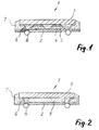
- a chip scale package 1 in two different ones Variants described.
- a preferably flexible carrier 2 made of plastic material, e.g. Polyimide film with a plurality of buffer cams 4 provided. These consist, for example, of a Silicone elastomer.
- a buffer cam 4 With help on this buffer cam an adhesive 5 attached to a silicon chip 3.
- On the free back of the carrier 2 are contact points in the shape of solder balls 8 arranged. These are about electrical Conductor 6 wired to the chip 3. All cavities between the buffer cams 4 and the area around the electrical conductors 6 are with a protective compound 7, for example filled out of plastic material.
- FIG. 2 differs the chip scale package 1 practically not from the outside that according to Figure 1. Instead of individual buffer cams however, a homogeneous adhesive layer 9 takes over Function of the buffer material and the spacer. After this Connect the electrical conductors 6 only in the Outside area are encapsulated with protective compound 7. The Danger of harmful influences from moisture thereby greatly reduced.
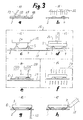
- Figure 3 shows the main workstations, their function is then explained.
- Figure 3a are at a Printing station using a stencil printing process individual Buffer cams printed on carrier 2.
- a template 18 is pressed against the carrier, which is provided with openings 21.
- a buffer mass 20 is pressed into the openings with a doctor blade 19, whereby the individual buffer cams are formed.
- the freshly formed buffer cams 4 are turned on according to Figure 3b a first hardening station 11 with a heat source 22.
- a carrier 2 prepared in this way now arrives on a Transport system 27 in a machine 26, in which side by side a dispensing station 12, a placement station 13 and optionally also a pre-hardening station 14 and / or a curing station 15 are arranged.
- a dispenser station 12 At the dispenser station 12 according to FIG. 3c is with a needle dispenser 23 an adhesive 5 from several tubes 24 simultaneously deposited each buffer cam 4. This will be an adhesive selected with the help of which gluing is carried out at room temperature can.
- the chip 3 is attached to the mounting station 13 according to FIG. 3d a placement head 25 on the coated buffer cams 4 discontinued. After a smooth, gentle onward transport a pre-hardening takes place to the pre-hardening station 14 according to FIG. 3e, preferably with the aid of infrared radiators 28, which irradiate the carrier 2 from above.
- Both stations that is Pre-hardening station and / or the hardening station could in certain cases may also be separate plant parts that are not can be run through with the same transport system.
- connection station 16 the electrical conductor 6 with a connecting tool 30 connected to the chip 3.
- This process (lead bonding) is already known per se to the person skilled in the art.
- the manufacturing process according to FIG. 4 works without the Formation of buffer cams.
- an adhesive 9 on the carrier 2 applied which also functions as a buffer mass takes over.
- the order is placed with the help of a movement dispenser 34, the one from a single needle 35 a certain Adhesive patterns, such as a cross or a star can draw on the carrier 2.
- the chip is placed on the adhesive 9 at the placement station 13 put on and with a small force against the carrier 2 pressed so that the previously drawn adhesive pattern under Displacement of the air forms a homogeneous layer.
- Pre-curing and / or curing in turn take place on the same way as in the previous embodiment.
- the wiring at station 16 is also the same.
- Figure 5 illustrates the arrangement of a group of settling positions on a carrier 2. Each position is with a plurality of buffer cams 4 provided. Such a thing The field of buffer cams is always with the needle dispenser according to FIG. 6 or in another way simultaneously with adhesive 5 coated.
- Figure 7 illustrates the size relationships, for example on the buffer cams. Accordingly, the diameter is a in the attachment area, for example, 450 ⁇ m and the maximum height b is 150 ⁇ m.
- the adhesive layer 5 has a maximum Diameter from about 350 to 450 microns, is therefore preferred slightly smaller than the area of the buffer cam.
- Figure 8 shows schematically an adjustment station 36, the immediate can be used at the touchdown station 13.
- the chip 3 becomes exact with the help of an adjustment optics 37 aligned with the underlying carrier 2 before or after he is discontinued.
- FIG. 9 schematically shows the rotary movement of a chip 3, between the removal of the wafer 38 and the placement on the Carrier.
- a pick-up arm 40 moves the chip from the wafer 38 a rotary holder 39.
- There the chip is turned and in next work cycle resumed from a delivery arm 41 and put down with the back against the carrier.
- FIG. 10 shows schematically how when the chip 3 is set down the mounting station of the carrier 2 by means of negative pressure on a Under pressure pad 42 can be fixed.
- the vacuum pad is provided with openings leading to a vacuum chamber to lead. There is a pressure below atmospheric lying pressure.
Landscapes
- Engineering & Computer Science (AREA)
- Microelectronics & Electronic Packaging (AREA)
- Computer Hardware Design (AREA)
- Power Engineering (AREA)
- Physics & Mathematics (AREA)
- Condensed Matter Physics & Semiconductors (AREA)
- General Physics & Mathematics (AREA)
- Manufacturing & Machinery (AREA)
- Wire Bonding (AREA)
- Die Bonding (AREA)
- Weting (AREA)
Priority Applications (12)
| Application Number | Priority Date | Filing Date | Title |
|---|---|---|---|
| EP99810009A EP1018760A1 (fr) | 1999-01-07 | 1999-01-07 | Procédé et dispositif pour encapsuler un dispositif électronique, spécialement une puce semi-conductrice |
| DE59909906T DE59909906D1 (de) | 1999-01-07 | 1999-07-02 | Verfahren und Vorrichtung zum Behandeln von auf einem Substrat angeordneten elektronischen Bauteilen, insbesondere von Halbleiterchips |
| PT99112660T PT1030349E (pt) | 1999-01-07 | 1999-07-02 | Processo e dispositivo para a manipulacao de pecas de construcao colocadas sobreum substrato particularmente chips semicondutores |
| AT99112660T ATE270790T1 (de) | 1999-01-07 | 1999-07-02 | Verfahren und vorrichtung zum behandeln von auf einem substrat angeordneten elektronischen bauteilen, insbesondere von halbleiterchips |
| ES99112660T ES2224501T3 (es) | 1999-01-07 | 1999-07-02 | Procedimiento y dispositivo para el tratamiento de componentes dispuestos sobre un substrato, especialmente de chips de semiconductores. |
| EP99112660.8A EP1030349B2 (fr) | 1999-01-07 | 1999-07-02 | Méthode et dispositif pour le traitement de composants électroniques montés sur substrat, en particulier de puces semi-conductrices |
| MYPI99005529A MY130850A (en) | 1999-01-07 | 1999-12-17 | Method and apparatus for treating electronic components mounted on a substrate, in particular semiconductor chips |
| JP2000592863A JP2002534799A (ja) | 1999-01-07 | 1999-12-22 | 基板上に配列された構成部品、特に半導体チップを加工処理するための方法及び装置 |
| PCT/CH1999/000620 WO2000041234A1 (fr) | 1999-01-07 | 1999-12-22 | Procede et dispositif pour encapsuler un composant electronique, en particulier une puce de semi-conducteur |
| KR1020017008579A KR20010108071A (ko) | 1999-01-07 | 1999-12-22 | 기판상에 배열된 구성 소자, 특히 반도체 칩을 처리하기위한 방법 및 장치 |
| PCT/CH1999/000621 WO2000041219A1 (fr) | 1999-01-07 | 1999-12-22 | Procede et dispositif de traitement de composants disposes sur un substrat, en particulier de puces de semi-conducteur |
| US09/478,411 US6621157B1 (en) | 1999-01-07 | 2000-01-06 | Method and device for encapsulating an electronic component in particular a semiconductor chip |
Applications Claiming Priority (1)
| Application Number | Priority Date | Filing Date | Title |
|---|---|---|---|
| EP99810009A EP1018760A1 (fr) | 1999-01-07 | 1999-01-07 | Procédé et dispositif pour encapsuler un dispositif électronique, spécialement une puce semi-conductrice |
Publications (1)
| Publication Number | Publication Date |
|---|---|
| EP1018760A1 true EP1018760A1 (fr) | 2000-07-12 |
Family
ID=8242628
Family Applications (1)
| Application Number | Title | Priority Date | Filing Date |
|---|---|---|---|
| EP99810009A Withdrawn EP1018760A1 (fr) | 1999-01-07 | 1999-01-07 | Procédé et dispositif pour encapsuler un dispositif électronique, spécialement une puce semi-conductrice |
Country Status (6)
| Country | Link |
|---|---|
| EP (1) | EP1018760A1 (fr) |
| AT (1) | ATE270790T1 (fr) |
| DE (1) | DE59909906D1 (fr) |
| ES (1) | ES2224501T3 (fr) |
| PT (1) | PT1030349E (fr) |
| WO (1) | WO2000041234A1 (fr) |
Cited By (1)
| Publication number | Priority date | Publication date | Assignee | Title |
|---|---|---|---|---|
| CN110740575A (zh) * | 2019-09-11 | 2020-01-31 | 黄诚 | 一种集成电路板生产加工设备 |
Families Citing this family (1)
| Publication number | Priority date | Publication date | Assignee | Title |
|---|---|---|---|---|
| DE10250778B3 (de) * | 2002-10-30 | 2004-03-04 | Infineon Technologies Ag | Elektronisches Bauteil mit einem Halbleiterchip und Verfahren zum Bestücken eines Schaltungsträgers beim Herstellen des elektronischen Bauteils |
Citations (4)
| Publication number | Priority date | Publication date | Assignee | Title |
|---|---|---|---|---|
| US5659952A (en) * | 1994-09-20 | 1997-08-26 | Tessera, Inc. | Method of fabricating compliant interface for semiconductor chip |
| WO1997033312A1 (fr) * | 1996-03-07 | 1997-09-12 | Tessera, Inc. | Procede d'encapsulation d'un emballage de semi-conducteur |
| EP0886313A1 (fr) * | 1996-12-04 | 1998-12-23 | Shinko Electric Industries Co. Ltd. | Dispositif a semi-conducteurs obture a la resine, fabrication dudit dispositif |
| EP0898305A2 (fr) * | 1997-08-20 | 1999-02-24 | Oki Electric Industry Co., Ltd. | Structure et procédé d'empaquetage de puces semi-conductrices |
-
1999
- 1999-01-07 EP EP99810009A patent/EP1018760A1/fr not_active Withdrawn
- 1999-07-02 PT PT99112660T patent/PT1030349E/pt unknown
- 1999-07-02 DE DE59909906T patent/DE59909906D1/de not_active Expired - Lifetime
- 1999-07-02 ES ES99112660T patent/ES2224501T3/es not_active Expired - Lifetime
- 1999-07-02 AT AT99112660T patent/ATE270790T1/de active
- 1999-12-22 WO PCT/CH1999/000620 patent/WO2000041234A1/fr active Search and Examination
Patent Citations (4)
| Publication number | Priority date | Publication date | Assignee | Title |
|---|---|---|---|---|
| US5659952A (en) * | 1994-09-20 | 1997-08-26 | Tessera, Inc. | Method of fabricating compliant interface for semiconductor chip |
| WO1997033312A1 (fr) * | 1996-03-07 | 1997-09-12 | Tessera, Inc. | Procede d'encapsulation d'un emballage de semi-conducteur |
| EP0886313A1 (fr) * | 1996-12-04 | 1998-12-23 | Shinko Electric Industries Co. Ltd. | Dispositif a semi-conducteurs obture a la resine, fabrication dudit dispositif |
| EP0898305A2 (fr) * | 1997-08-20 | 1999-02-24 | Oki Electric Industry Co., Ltd. | Structure et procédé d'empaquetage de puces semi-conductrices |
Non-Patent Citations (1)
| Title |
|---|
| MITCHELL C: "Advancements in CSP encapsulation: Process and material", PAN PACIFIC MICROELECTRONICS SYMPOSIUM. PROCEEDINGS OF THE TECHNICAL PROGRAM, PROCEEDINGS OF PAN PACIFIC MICROELECTRONICS SYMPOSIUM, KONA, HI, USA, 10-13 FEB. 1998, 1998, EDINA, MN, USA, SURFACE MOUNT TECHNOL. ASSOC, USA, PAGE(S) 137 - 140, XP002107244 * |
Cited By (1)
| Publication number | Priority date | Publication date | Assignee | Title |
|---|---|---|---|---|
| CN110740575A (zh) * | 2019-09-11 | 2020-01-31 | 黄诚 | 一种集成电路板生产加工设备 |
Also Published As
| Publication number | Publication date |
|---|---|
| ATE270790T1 (de) | 2004-07-15 |
| ES2224501T3 (es) | 2005-03-01 |
| DE59909906D1 (de) | 2004-08-12 |
| PT1030349E (pt) | 2004-11-30 |
| WO2000041234A1 (fr) | 2000-07-13 |
Similar Documents
| Publication | Publication Date | Title |
|---|---|---|
| EP1030349B1 (fr) | Méthode et dispositif pour le traitement de composants électroniques montés sur substrat, en particulier de puces semi-conductrices | |
| DE10334576B4 (de) | Verfahren zum Herstellen eines Halbleiterbauelements mit einem Kunststoffgehäuse | |
| DE69532682T2 (de) | Nachgiebige zwischenschicht für einen halbleiterchip | |
| EP1796137B1 (fr) | Appareil et méthode cadencée pour frittage sous pression | |
| DE3805572C2 (de) | Trägerband für elektronische Bauelemente sowie Verfahren zum Herstellen einer Folge von elektronischen Bauelementen | |
| DE1591186B1 (de) | Verfahren zum simultanen Herstellen von Zufuehrungs-verbindungen mittels Kontaktbruecken auf Festkoerperbauelementen mit Hilfe von abziehbildartigen Vorrichtungen | |
| DE10102197A1 (de) | Verbessertes Verfahren zum Herstellen eines Chip-Bauelements | |
| DE19628237A1 (de) | Halbleitervorrichtung und Herstellungsverfahren der Gleichen | |
| CH640993A5 (de) | Verfahren zum befestigen von chip-artigen schaltungselementen auf einer platte fuer gedruckte schaltungen sowie vorrichtung zur durchfuehrung dieses verfahrens. | |
| DE19723202A1 (de) | Rißfestes Halbleiterbauteil sowie Herstellungsverfahren und Herstellungsgerät hierfür | |
| DE102008033651B4 (de) | Verfahren zur Herstellung eines Leistungshalbleitermoduls | |
| DE102011114015A1 (de) | Endeffektor | |
| WO2013174418A1 (fr) | Procédé de fabrication d'un module électronique | |
| DE60207282T2 (de) | Verkapselung des anschlusslots zur aufrechterhaltung der genauigkeit der anschlussposition | |
| WO2001063605A1 (fr) | Procede et dispositif pour produire un dvd | |
| EP0002496A1 (fr) | Méthode et appareil pour aligner des pièces à usiner minces et plates | |
| EP1204137A2 (fr) | Méthode et appareil pour contacter des puces semi-conductrices | |
| EP1398828A2 (fr) | Boítier semi-conducteur avec polymère d'encapsulation pré-réticulé et son procédé de fabrication | |
| DE102005015036B4 (de) | Verfahren zur Montage eines Chips auf einer Unterlage | |
| DE2108850C2 (de) | Verfahren zur Befestigung von Zuleitungen an Halbleiterplättchen | |
| EP1018760A1 (fr) | Procédé et dispositif pour encapsuler un dispositif électronique, spécialement une puce semi-conductrice | |
| DE102005006978B3 (de) | Verfahren und Vorrichtung zum Verbinden von Halbleiterelementen oder Interposern mit einem Trägerband und Verwendung einer derartigen Vorrichtung | |
| WO1996002955A1 (fr) | Procede de realisation d'une connexion electro-conductrice | |
| DE19819054B4 (de) | Verfahren und Vorrichtung zur Montage und Justierung von Bauteilen auf einer Befestigungsunterlage | |
| EP0644507B1 (fr) | Méthode et procédé de fabrication de modules pour carte à puce |
Legal Events
| Date | Code | Title | Description |
|---|---|---|---|
| PUAI | Public reference made under article 153(3) epc to a published international application that has entered the european phase |
Free format text: ORIGINAL CODE: 0009012 |
|
| AK | Designated contracting states |
Kind code of ref document: A1 Designated state(s): AT CH DE FI FR GB IT LI NL PT SE |
|
| AX | Request for extension of the european patent |
Free format text: AL;LT;LV;MK;RO;SI |
|
| 17P | Request for examination filed |
Effective date: 20001009 |
|
| AKX | Designation fees paid |
Free format text: AT CH DE FI FR GB IT LI NL PT SE |
|
| AXX | Extension fees paid |
Free format text: LT PAYMENT 20001009;LV PAYMENT 20001009 |
|
| STAA | Information on the status of an ep patent application or granted ep patent |
Free format text: STATUS: THE APPLICATION IS DEEMED TO BE WITHDRAWN |
|
| 18D | Application deemed to be withdrawn |
Effective date: 20020801 |