EP1005083A1 - Elektronisches Leistungselement mit Kühlvorrichtung - Google Patents
Elektronisches Leistungselement mit Kühlvorrichtung Download PDFInfo
- Publication number
- EP1005083A1 EP1005083A1 EP99402890A EP99402890A EP1005083A1 EP 1005083 A1 EP1005083 A1 EP 1005083A1 EP 99402890 A EP99402890 A EP 99402890A EP 99402890 A EP99402890 A EP 99402890A EP 1005083 A1 EP1005083 A1 EP 1005083A1
- Authority
- EP
- European Patent Office
- Prior art keywords
- opposite
- layer
- semiconductor
- composite structure
- semiconductor circuit
- Prior art date
- Legal status (The legal status is an assumption and is not a legal conclusion. Google has not performed a legal analysis and makes no representation as to the accuracy of the status listed.)
- Granted
Links
Images


Classifications
-
- H—ELECTRICITY
- H05—ELECTRIC TECHNIQUES NOT OTHERWISE PROVIDED FOR
- H05K—PRINTED CIRCUITS; CASINGS OR CONSTRUCTIONAL DETAILS OF ELECTRIC APPARATUS; MANUFACTURE OF ASSEMBLAGES OF ELECTRICAL COMPONENTS
- H05K7/00—Constructional details common to different types of electric apparatus
- H05K7/20—Modifications to facilitate cooling, ventilating, or heating
-
- H—ELECTRICITY
- H10—SEMICONDUCTOR DEVICES; ELECTRIC SOLID-STATE DEVICES NOT OTHERWISE PROVIDED FOR
- H10W—GENERIC PACKAGES, INTERCONNECTIONS, CONNECTORS OR OTHER CONSTRUCTIONAL DETAILS OF DEVICES COVERED BY CLASS H10
- H10W40/00—Arrangements for thermal protection or thermal control
- H10W40/40—Arrangements for thermal protection or thermal control involving heat exchange by flowing fluids
- H10W40/47—Arrangements for thermal protection or thermal control involving heat exchange by flowing fluids by flowing liquids, e.g. forced water cooling
-
- H—ELECTRICITY
- H10—SEMICONDUCTOR DEVICES; ELECTRIC SOLID-STATE DEVICES NOT OTHERWISE PROVIDED FOR
- H10W—GENERIC PACKAGES, INTERCONNECTIONS, CONNECTORS OR OTHER CONSTRUCTIONAL DETAILS OF DEVICES COVERED BY CLASS H10
- H10W90/00—Package configurations
Definitions
- the present invention relates to an electronic component power.
- the electronic components of power which are used in particular to achieve inverters for rail traction, include a sole made for example of copper.
- a multiplicity of conductor-insulator-conductor type composite structures which assume both a heat transfer function and electrical insulation, are reported on this sole. They are for example produced in the form of a stack copper-ceramic-copper also known as Direct Bonded Copper (DBC).
- DBC Direct Bonded Copper
- These composite structures can also be made in the form of insulated metal substrates (SMI) which include a bottom layer of aluminum or copper, an intermediate layer of epoxy and an upper layer of copper possibly made in several parts.
- SBI insulated metal substrates
- each composite structure On each composite structure are arranged several power semiconductor circuits, which are for example insulated gate bipolar transistors called IGBTs, or more diodes. These semiconductor circuits are further covered on one of their faces by connection pads, and are subject to the free metallic layer of the structure composite by their face free of studs. These circuits are there fixed for example by soft tin-lead solder or tin-lead-silver.
- IGBTs insulated gate bipolar transistors
- connection pad we solder, on each connection pad, several aluminum wire typically having a diameter of 380 to 500 microns. Each of these wires is also soldered to the upper metallic layer of the composite structure.
- This unit formed by the sole, the composite structures and the semiconductor power circuits, is then arranged in a case filled with silicone gel and covered with a cover made of epoxy resin, so as to form an electronic component power.
- a cooling element which can be a water plate, a air heat exchanger or an evaporator base "heat pipe”.
- a cooling element is intended to maintain the temperature to which the electronic component of power at a value lower than 125 ° C, so as to maintain integrity.
- the cooling problem is all particularly crucial in the area of components power electronics, to the extent that it is this threshold temperature of around 125 ° C which determines the value of current admissible by the component.
- the invention therefore aims to improve cooling electronic power components, so either increase the current handling of these components for a volume and therefore a given cost price, or to be reduced, for a given nominal current, the volume and therefore the cost price.
- the invention more particularly proposes to carry out a power electronic component whose structure be different from that of the components of art anterior, and thereby improves cooling.
- the invention relates to a component power electronics comprising a first structure composite of thermal transfer and electrical insulation, supporting at least one semiconductor power circuit whose face opposite to said first composite structure is provided with connection pads, said first structure composite comprising two conductive or semi-conductive layers respectively adjacent and opposite to said semiconductor circuit , characterized in that said connection pads are subject, by their face opposite to said first composite structure, to a plane network of conductive elements isolated from each other, said network being integrated into at least one second composite heat transfer and insulation structure electric, which has a conductive or semi-conductive layer opposite to said semiconductor circuit, and in that the opposite layer of at least one of the first or second composite structure includes means for passing a fluid coolant.
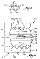
- Figures 1 to 3 illustrate the manufacture of a semiconductor layer intended to be integrated into a power electronic component according to the invention.
- This manufacture firstly uses two wafers shown in Figure 1 and conventionally called first wafer 2 and second wafer 4, which are made of monocrystalline silicon. They have dimensions similar to each other, namely that they have a thickness e of approximately 1 mm and main dimensions of approximately 50 by 50 mm.
- the next step is to perform grooves 6 within the first plate 2.
- These grooves are executed, in a manner known per se, through of a wet etching process by chemical attack. Being given the nature of monocrystalline silicon, this operation is particularly easy and leads to the formation of grooves with a U-shaped profile with inclined wings, the engraving taking place following the crystal planes.
- the angle ⁇ defining the inclination of the wings 6A of the grooves is close to 57 °.
- the etching operation is stopped when the depth p of the groove 6 is equal to approximately half of its width L.
- approximately 50 grooves are executed on the wafer 2, which corresponds to a density of about 10 grooves per cm.
- the grooves 6 can also have a V shape.
- FIG 2 illustrates only the realization of the grooves 6 at the wafer 2, it being understood that in the mode of execution described, we realize at the level of the second plate 4 of similar grooves which will be designated by the reference 8 in the following.
- the next step is to assemble the two plates 2 and 4.
- the layer formed by the assembly of the two plates 2 and 4 is designated as a whole by the reference 10. It is provided with a multiplicity of channels 12 produced by cooperation shapes of grooves 6 and 8 opposite, which are provided in the respective plates 2 and 4. These channels 12 extend on either side of the joint plane P between the two plates 2, 4, have a substantially hexagonal shape and have a width L substantially equal to their height H. These channels are through, or through, namely that they extend between two opposite edges of layer 10.
- grooves are made within of the two plates 2 and 4. It is also possible to plan to execute such grooves on a single plate, the channels being formed by these grooves and the flat surface of the other plate.
- Figure 5 illustrates a next phase of realization a power electronic component according to the invention, phase which consists first of all in coating the free face studs 23 by means of a multilayer 24 of titanium-nickel-gold whose thickness is approximately 0.8 micrometers and which is deposited for example by means of a spraying process.
- this multilayer 24 there is a boss 26 produced in tin-lead-silver, the size of which corresponds to that of the stud 12. In the example considered, this boss has a composition about 2% tin, 95.5% lead and 2.5% silver. It should be noted that the presence of the multilayer 24 gives a excellent mechanical strength of the boss 26 on the stud 23.
- This structure 119 comprises layers 110 and 116 identical to those 10 and 16 of structure 19.
- Layer 116 is covered by a planar network 118 of conductive elements isolated from each other, whose configuration is adapted to that of the semiconductor circuit 20 that this planar network 118 must cover.
- the power electronic component thus formed and designated as a whole by the reference 28 is then able to be cooled both for the middle of layers 10 and 110.
- channels 12 and 112 of which the latter are respectively provided are intended for the passage of a fluid gaseous or liquid coolant and are therefore relationship with a source of such a fluid.
- the conformation of the electronic power component 28 of the invention also makes it possible to overcome the presence aluminum wires which are usually provided with components of the prior art.
- the plan 118 of the second composite structure 119 usually assumes the role devoted to these aluminum wires.
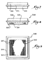
- Figures 7 to 9 show the execution of another composite structure intended to be integrated into a component power electronics according to the invention.
- This production first of all uses a structure conductor-insulator-conductor composite in its usual conformation, shown in Figure 7.
- This structure comprises a first layer 202, or lower layer made for example of copper and surmounted by a insulating layer 204 intermediate supporting a second metallic layer 206, or upper layer, also in copper.
- the conductive layers 202 and 206 have by example a thickness of 3 to 4 mm and main dimensions 48 x 48 mm, while the insulating layer 204 has a thickness of 0.635 mm and main dimensions of 50 x 50 mm.
- Figures 8 and 9 show a composite structure intended to be integrated into a component according to the invention, structure designated as a whole by the reference 208 and which was made from the structure shown in Figure 7.
- the lower layer 202 of this structure 208 is provided with a multiplicity of channels or conduits 210 intended to constitute means for the passage of a heat transfer fluid.
- These channels are made parallel to one of the dimensions principal of the lower layer 202, starting from the face bottom of the latter, as shown in particular by the figure 8.
- Each of these channels extends over a substantial part the thickness of this lower layer 2, that is to say for example over a height between 2 and 3 mm.
- these channels is for example 200 micrometers and their length between 40 and 50 mm.
- these channels 210 are provided in the number of approximately 50, of so that two neighboring channels are spaced a distance apart between 200 and 300 micrometers.
- Layer 304 is further covered by a flat network 306 conductive elements isolated from each other, the configuration of which is adapted to that of the semiconductor circuit 220 that this plan network overlaps.
- the pads 223 are then subject to the plan network 306 of the second composite structure 308, network 306 which will be called adjacent as opposed to layer 302 called opposite.
- the power electronic component thus formed is then at even to be cooled both through the layers 202, 302 opposite the semiconductor circuit 220.
- the channels 210, 310 formed in the latter are specific to the passage of a gaseous or liquid heat transfer fluid and are, at this effect put in relation with a source of such a fluid.
- the channels lead to the distal face of layers 202 and 302, namely their most distant from the semiconductor circuit 220.
- the power electronic component according to the invention achieves the previously mentioned objectives. Indeed, it allows to get rid of the presence of wires aluminum with which the components of the prior art are provided.
- these threads constitute a limiting factor with regard to the cooling problem, as they heat up proportional to the square of the current which crosses, and it turns out to be difficult to cool it since they are embedded in silicone gel.
- these sons aluminum can cause serious malfunctions of the entire electronic power component. In indeed, they are subjected, in service, to thermal cycling, so that they are able to break.
- the component of the invention apart from that it is devoid of such aluminum wire, provides double cooling power semiconductor circuits simultaneously compose, both from their lower and upper faces.
- the composite structures forming the component according to the invention assume, in addition to their usual functions heat transfer and electrical insulation, additional cooling function. This therefore allows limit the number of interfaces between the different layers constituting the component of the invention, since the element of cooling is integrated into each composite structure. This also has the effect of increasing the exchange coefficient convective with the heat transfer fluid circulating in the channels formed in the opposite layer of each composite structure.
- the component according to the invention has a current withstand significantly higher.
Landscapes
- Physics & Mathematics (AREA)
- Thermal Sciences (AREA)
- Engineering & Computer Science (AREA)
- Microelectronics & Electronic Packaging (AREA)
- Cooling Or The Like Of Semiconductors Or Solid State Devices (AREA)
- Cooling Or The Like Of Electrical Apparatus (AREA)
- Control Of Electric Motors In General (AREA)
Priority Applications (1)
| Application Number | Priority Date | Filing Date | Title |
|---|---|---|---|
| DK99402890T DK1005083T3 (da) | 1998-11-27 | 1999-11-22 | Elektronisk effektkomponent, som omfatter en afkölingsanordning |
Applications Claiming Priority (2)
| Application Number | Priority Date | Filing Date | Title |
|---|---|---|---|
| FR9815155A FR2786656B1 (fr) | 1998-11-27 | 1998-11-27 | Composant electronique de puissance comportant des moyens de refroidissement |
| FR9815155 | 1998-11-27 |
Publications (2)
| Publication Number | Publication Date |
|---|---|
| EP1005083A1 true EP1005083A1 (de) | 2000-05-31 |
| EP1005083B1 EP1005083B1 (de) | 2004-07-14 |
Family
ID=9533441
Family Applications (1)
| Application Number | Title | Priority Date | Filing Date |
|---|---|---|---|
| EP99402890A Expired - Lifetime EP1005083B1 (de) | 1998-11-27 | 1999-11-22 | Elektronisches Leistungselement mit Kühlvorrichtung |
Country Status (13)
| Country | Link |
|---|---|
| US (1) | US6344686B1 (de) |
| EP (1) | EP1005083B1 (de) |
| JP (1) | JP2000164780A (de) |
| KR (1) | KR100603880B1 (de) |
| CN (1) | CN1146041C (de) |
| AT (1) | ATE271259T1 (de) |
| AU (1) | AU755407B2 (de) |
| CA (1) | CA2290802C (de) |
| DE (1) | DE69918644T2 (de) |
| DK (1) | DK1005083T3 (de) |
| ES (1) | ES2222674T3 (de) |
| FR (1) | FR2786656B1 (de) |
| PT (1) | PT1005083E (de) |
Cited By (2)
| Publication number | Priority date | Publication date | Assignee | Title |
|---|---|---|---|---|
| WO2008154265A1 (en) * | 2007-06-08 | 2008-12-18 | Continental Automotive Systems Us, Inc. | Insulated gate bipolar transistor assembly |
| EP3410478A1 (de) * | 2017-05-29 | 2018-12-05 | Mitsubishi Electric R & D Centre Europe B.V. | Leistungsmodul und verfahren zur herstellung des leistungsmoduls |
Families Citing this family (16)
| Publication number | Priority date | Publication date | Assignee | Title |
|---|---|---|---|---|
| WO2001050526A1 (en) * | 1999-12-30 | 2001-07-12 | Intel Corporation | Optimized driver layout for integrated circuits with staggered bond pads |
| US6773963B2 (en) * | 2002-01-16 | 2004-08-10 | Intel Corporation | Apparatus and method for containing excess thermal interface material |
| US6903929B2 (en) * | 2003-03-31 | 2005-06-07 | Intel Corporation | Two-phase cooling utilizing microchannel heat exchangers and channeled heat sink |
| US6934154B2 (en) * | 2003-03-31 | 2005-08-23 | Intel Corporation | Micro-channel heat exchangers and spreaders |
| JP4491244B2 (ja) * | 2004-01-07 | 2010-06-30 | 三菱電機株式会社 | 電力半導体装置 |
| US7353859B2 (en) * | 2004-11-24 | 2008-04-08 | General Electric Company | Heat sink with microchannel cooling for power devices |
| US7327024B2 (en) * | 2004-11-24 | 2008-02-05 | General Electric Company | Power module, and phase leg assembly |
| JP4478049B2 (ja) * | 2005-03-15 | 2010-06-09 | 三菱電機株式会社 | 半導体装置 |
| DE102005050028A1 (de) | 2005-10-14 | 2007-04-19 | Robert Bosch Gmbh | Elektrische Vorrichtung, insbesondere zur Ansteuerung einer motorisch und/oder generatorisch betreibbaren elektrischen Maschine |
| US20070158050A1 (en) * | 2006-01-06 | 2007-07-12 | Julian Norley | Microchannel heat sink manufactured from graphite materials |
| US7898807B2 (en) * | 2009-03-09 | 2011-03-01 | General Electric Company | Methods for making millichannel substrate, and cooling device and apparatus using the substrate |
| US8232637B2 (en) * | 2009-04-30 | 2012-07-31 | General Electric Company | Insulated metal substrates incorporating advanced cooling |
| WO2012058105A1 (en) * | 2010-10-28 | 2012-05-03 | Spx Cooling Technologies, Inc. | Heat exchanger fin, roll forming die assembly for forming same, and method of forming |
| JP5891707B2 (ja) * | 2011-10-28 | 2016-03-23 | 富士通株式会社 | 半導体装置とその製造方法 |
| KR101692490B1 (ko) | 2015-08-11 | 2017-01-04 | 주식회사 세미파워렉스 | 액체냉각구조를 갖는 전력반도체 모듈 |
| KR102869892B1 (ko) | 2023-11-20 | 2025-10-14 | 주식회사 세미파워렉스 | 일체형 냉각구조를 갖는 전력반도체모듈 및 그 제조방법 |
Citations (3)
| Publication number | Priority date | Publication date | Assignee | Title |
|---|---|---|---|---|
| DE4311839A1 (de) * | 1993-04-15 | 1994-10-20 | Siemens Ag | Mikrokühleinrichtung für eine Elektronik-Komponente |
| FR2737608A1 (fr) * | 1995-08-02 | 1997-02-07 | Alsthom Cge Alcatel | Dispositif electronique de puissance pourvu de moyens ameliores d'evacuation de la chaleur |
| EP0871352A1 (de) * | 1997-03-28 | 1998-10-14 | Nec Corporation | Aufbau zum Kühlen einer integrierten Schaltung |
Family Cites Families (20)
| Publication number | Priority date | Publication date | Assignee | Title |
|---|---|---|---|---|
| US3663184A (en) * | 1970-01-23 | 1972-05-16 | Fairchild Camera Instr Co | Solder bump metallization system using a titanium-nickel barrier layer |
| US3652903A (en) * | 1971-02-01 | 1972-03-28 | Gen Electric | Fluid cooled pressure assembly |
| DE2160001C2 (de) * | 1971-12-03 | 1974-01-10 | Siemens Ag, 1000 Berlin U. 8000 Muenchen | Halbleiteranordnung, insbesondere Thyristorbaugruppe |
| DE2813529A1 (de) * | 1978-03-29 | 1979-10-04 | Siemens Ag | Anordnung zur beidseitigen kuehlung von halbleiterbauelementen |
| US4392153A (en) * | 1978-05-01 | 1983-07-05 | General Electric Company | Cooled semiconductor power module including structured strain buffers without dry interfaces |
| US4520305A (en) * | 1983-08-17 | 1985-05-28 | Cauchy Charles J | Thermoelectric generating system |
| US4774630A (en) * | 1985-09-30 | 1988-09-27 | Microelectronics Center Of North Carolina | Apparatus for mounting a semiconductor chip and making electrical connections thereto |
| US4758926A (en) * | 1986-03-31 | 1988-07-19 | Microelectronics And Computer Technology Corporation | Fluid-cooled integrated circuit package |
| US4879629A (en) * | 1988-10-31 | 1989-11-07 | Unisys Corporation | Liquid cooled multi-chip integrated circuit module incorporating a seamless compliant member for leakproof operation |
| JP2891432B2 (ja) * | 1989-12-27 | 1999-05-17 | 田中電子工業株式会社 | 半導体材料の接続方法,それに用いる接続材料及び半導体装置 |
| US5168537A (en) * | 1991-06-28 | 1992-12-01 | Digital Equipment Corporation | Method and apparatus for coupling light between an optoelectronic device and a waveguide |
| US5323292A (en) * | 1992-10-06 | 1994-06-21 | Hewlett-Packard Company | Integrated multi-chip module having a conformal chip/heat exchanger interface |
| FR2701600B1 (fr) * | 1993-02-10 | 1995-09-08 | Gec Alsthom Transport Sa | Dispositif de refroidissement de composants electriques de puissance. |
| JP3152834B2 (ja) * | 1993-06-24 | 2001-04-03 | 株式会社東芝 | 電子回路装置 |
| US5829516A (en) * | 1993-12-15 | 1998-11-03 | Aavid Thermal Products, Inc. | Liquid cooled heat sink for cooling electronic components |
| US5504378A (en) * | 1994-06-10 | 1996-04-02 | Westinghouse Electric Corp. | Direct cooled switching module for electric vehicle propulsion system |
| US5774334A (en) * | 1994-08-26 | 1998-06-30 | Hitachi, Ltd. | Low thermal resistant, fluid-cooled semiconductor module |
| JPH08241943A (ja) * | 1995-03-07 | 1996-09-17 | Fuji Electric Co Ltd | パワー半導体素子用の液冷式冷却体 |
| US5831336A (en) * | 1996-07-25 | 1998-11-03 | International Business Machines Corporation | Ternary solder for the enhancement of C-4 fatigue life |
| US5790376A (en) * | 1996-11-06 | 1998-08-04 | Compaq Computer Corporation | Heat dissipating pad structure for an electronic component |
-
1998
- 1998-11-27 FR FR9815155A patent/FR2786656B1/fr not_active Expired - Fee Related
-
1999
- 1999-11-22 DK DK99402890T patent/DK1005083T3/da active
- 1999-11-22 ES ES99402890T patent/ES2222674T3/es not_active Expired - Lifetime
- 1999-11-22 PT PT99402890T patent/PT1005083E/pt unknown
- 1999-11-22 EP EP99402890A patent/EP1005083B1/de not_active Expired - Lifetime
- 1999-11-22 AT AT99402890T patent/ATE271259T1/de active
- 1999-11-22 DE DE69918644T patent/DE69918644T2/de not_active Expired - Lifetime
- 1999-11-23 US US09/447,832 patent/US6344686B1/en not_active Expired - Lifetime
- 1999-11-23 AU AU59610/99A patent/AU755407B2/en not_active Expired
- 1999-11-24 CA CA002290802A patent/CA2290802C/fr not_active Expired - Lifetime
- 1999-11-26 CN CNB991243870A patent/CN1146041C/zh not_active Expired - Lifetime
- 1999-11-26 JP JP11335356A patent/JP2000164780A/ja active Pending
- 1999-11-26 KR KR1019990052891A patent/KR100603880B1/ko not_active Expired - Lifetime
Patent Citations (3)
| Publication number | Priority date | Publication date | Assignee | Title |
|---|---|---|---|---|
| DE4311839A1 (de) * | 1993-04-15 | 1994-10-20 | Siemens Ag | Mikrokühleinrichtung für eine Elektronik-Komponente |
| FR2737608A1 (fr) * | 1995-08-02 | 1997-02-07 | Alsthom Cge Alcatel | Dispositif electronique de puissance pourvu de moyens ameliores d'evacuation de la chaleur |
| EP0871352A1 (de) * | 1997-03-28 | 1998-10-14 | Nec Corporation | Aufbau zum Kühlen einer integrierten Schaltung |
Non-Patent Citations (3)
| Title |
|---|
| CONFERENCE RECORD OF 1998 IEEE INDUSTRY APPLICATIONS CONFERENCE. THIRTY-THIRD IAS ANNUAL MEETING (CAT. NO.98CH36242), CONFERENCE RECORD OF 1998 IEEE INDUSTRY APPLICATIONS CONFERENCE. THIRTY-THIRD IAS ANNUAL MEETING, ST. LOUIS, MO, USA, 12-15 OCT. 199, 1998, New York, NY, USA, IEEE, USA, pages 1051 - 1055 vol.2, ISBN: 0-7803-4943-1 * |
| DATABASE INSPEC [online] INSTITUTE OF ELECTRICAL ENGINEERS, STEVENAGE, GB; PERRET C ET AL: "Microchannel integrated heat sinks in silicon technology", XP002108745, Database accession no. 6161880 * |
| KAZUO TSUBOUCHI ET AL: "THEORETICAL ANALYSIS FOR A NEW PACKAGE CONCEPT: HIGH-SPEED HEAT REMOVAL FOR VLSI USING AN AIN HEAT-SPREADING LAYER AND MICROCHANNEL FIN", JAPANESE JOURNAL OF APPLIED PHYSICS, VOL. 30, NR. 1B, PAGE(S) L88 - L91, ISSN: 0021-4922, XP000223790 * |
Cited By (4)
| Publication number | Priority date | Publication date | Assignee | Title |
|---|---|---|---|---|
| WO2008154265A1 (en) * | 2007-06-08 | 2008-12-18 | Continental Automotive Systems Us, Inc. | Insulated gate bipolar transistor assembly |
| US7973387B2 (en) | 2007-06-08 | 2011-07-05 | Continental Automotive Systems Us, Inc. | Insulated gate bipolar transistor |
| EP3410478A1 (de) * | 2017-05-29 | 2018-12-05 | Mitsubishi Electric R & D Centre Europe B.V. | Leistungsmodul und verfahren zur herstellung des leistungsmoduls |
| WO2018221149A1 (en) * | 2017-05-29 | 2018-12-06 | Mitsubishi Electric Corporation | Power module and method for manufacturing the power module |
Also Published As
| Publication number | Publication date |
|---|---|
| FR2786656A1 (fr) | 2000-06-02 |
| CA2290802C (fr) | 2008-08-05 |
| DE69918644D1 (de) | 2004-08-19 |
| EP1005083B1 (de) | 2004-07-14 |
| AU755407B2 (en) | 2002-12-12 |
| CN1258934A (zh) | 2000-07-05 |
| CN1146041C (zh) | 2004-04-14 |
| ES2222674T3 (es) | 2005-02-01 |
| FR2786656B1 (fr) | 2001-01-26 |
| US6344686B1 (en) | 2002-02-05 |
| DK1005083T3 (da) | 2004-11-22 |
| PT1005083E (pt) | 2004-10-29 |
| KR100603880B1 (ko) | 2006-07-24 |
| KR20000035714A (ko) | 2000-06-26 |
| JP2000164780A (ja) | 2000-06-16 |
| CA2290802A1 (fr) | 2000-05-27 |
| ATE271259T1 (de) | 2004-07-15 |
| DE69918644T2 (de) | 2005-07-21 |
| AU5961099A (en) | 2000-06-01 |
Similar Documents
| Publication | Publication Date | Title |
|---|---|---|
| EP1005083B1 (de) | Elektronisches Leistungselement mit Kühlvorrichtung | |
| CA2290801C (fr) | Dispositif electronique de puissance | |
| EP1025584B1 (de) | Elektronische integrierte schaltung mit mindestens einem elektronischen bauelement | |
| US6552405B2 (en) | Photoelectric conversion device and manufacturing method thereof | |
| FR2813440A1 (fr) | Dispositif a semiconducteur pour la commande d'energie electrique | |
| FR2879021A1 (fr) | Dispositif a semiconducteur de puissance | |
| EP1168906B1 (de) | Elektronisches Leistungsmodul mit elektronischen Hochleistungsbauteilen und zugehöriges Herstellungsverfahren | |
| FR2786657A1 (fr) | Composant electronique de puissance comportant des moyens de refroidissement et procede de fabrication d'un tel composant | |
| CA2352513A1 (fr) | Procede de fabrication d'un composant electronique de puissance, et composant electronique de puissance ainsi obtenu | |
| EP3714669B1 (de) | Leistungselektronikmodul | |
| EP1189277A1 (de) | Elektronikschaltungssubstrat und Elektronikmodul damit | |
| EP1239515B1 (de) | Substrat für elektronische Leistungsschaltung und elektronisches Leistungsmodul mit diesem | |
| FR2514565A1 (fr) | Ensemble a pile solaire et procede de fixation d'une barre omnibus a une pile solaire | |
| EP0446125B1 (de) | Leistungshalbleiteranordnung | |
| EP1035573A1 (de) | Elektrisches Leistungsbauelement auf einen Träger gelötet und Montierungsverfahren dafür | |
| FR2786658A1 (fr) | Structure composite pour composant electronique de puissance procede de fabrication de cette structure et composant electronique de puissance pourvu d'une telle structure | |
| EP0734066B1 (de) | Elektronischer Leistungsmodul | |
| EP3242322B1 (de) | Elektronische leistungsvorrichtung mit flacher elektrischer verbindungsstruktur | |
| FR2571921A1 (fr) | Dissipateur de chaleur pour composants electroniques avec substrat en ceramique | |
| EP4150751A1 (de) | Elektrisches modul mit umspritzung und systeme mit solch einem elektrischen modul | |
| FR2699039A1 (fr) | Carte électronique à substrat multicouche. | |
| FR3144399A1 (fr) | Module électronique de puissance multi-étages | |
| FR3144483A1 (fr) | Module électronique de puissance multi-étages et hermétique | |
| FR3110035A1 (fr) | Module electrique avec surmoulage et dispositifs comprenant un tel module electrique | |
| EP0119134A1 (de) | Zusammenbau-Anordnung für elektronische Leistungsbauelemente auf einem Kühlkörper und Anwendung für Monophasen- oder Polyphasen-Brücken |
Legal Events
| Date | Code | Title | Description |
|---|---|---|---|
| PUAI | Public reference made under article 153(3) epc to a published international application that has entered the european phase |
Free format text: ORIGINAL CODE: 0009012 |
|
| AK | Designated contracting states |
Kind code of ref document: A1 Designated state(s): AT BE CH CY DE DK ES FI FR GB GR IE IT LI LU MC NL PT SE |
|
| AX | Request for extension of the european patent |
Free format text: AL;LT;LV;MK;RO;SI |
|
| 17P | Request for examination filed |
Effective date: 20001130 |
|
| AKX | Designation fees paid |
Free format text: AT BE CH CY DE DK ES FI FR GB GR IE IT LI LU MC NL PT SE |
|
| GRAP | Despatch of communication of intention to grant a patent |
Free format text: ORIGINAL CODE: EPIDOSNIGR1 |
|
| GRAS | Grant fee paid |
Free format text: ORIGINAL CODE: EPIDOSNIGR3 |
|
| GRAA | (expected) grant |
Free format text: ORIGINAL CODE: 0009210 |
|
| AK | Designated contracting states |
Kind code of ref document: B1 Designated state(s): AT BE CH CY DE DK ES FI FR GB GR IE IT LI LU MC NL PT SE |
|
| PG25 | Lapsed in a contracting state [announced via postgrant information from national office to epo] |
Ref country code: CY Free format text: LAPSE BECAUSE OF FAILURE TO SUBMIT A TRANSLATION OF THE DESCRIPTION OR TO PAY THE FEE WITHIN THE PRESCRIBED TIME-LIMIT Effective date: 20040714 |
|
| REG | Reference to a national code |
Ref country code: GB Ref legal event code: FG4D Free format text: NOT ENGLISH |
|
| REG | Reference to a national code |
Ref country code: CH Ref legal event code: EP |
|
| REF | Corresponds to: |
Ref document number: 69918644 Country of ref document: DE Date of ref document: 20040819 Kind code of ref document: P |
|
| REG | Reference to a national code |
Ref country code: IE Ref legal event code: FG4D Free format text: FRENCH |
|
| REG | Reference to a national code |
Ref country code: CH Ref legal event code: NV Representative=s name: CABINET ROLAND NITHARDT CONSEILS EN PROPRIETE INDU |
|
| GBT | Gb: translation of ep patent filed (gb section 77(6)(a)/1977) |
Effective date: 20040909 |
|
| REG | Reference to a national code |
Ref country code: SE Ref legal event code: TRGR |
|
| REG | Reference to a national code |
Ref country code: GR Ref legal event code: EP Ref document number: 20040402875 Country of ref document: GR |
|
| REG | Reference to a national code |
Ref country code: PT Ref legal event code: SC4A Free format text: AVAILABILITY OF NATIONAL TRANSLATION Effective date: 20040827 |
|
| PG25 | Lapsed in a contracting state [announced via postgrant information from national office to epo] |
Ref country code: LU Free format text: LAPSE BECAUSE OF NON-PAYMENT OF DUE FEES Effective date: 20041122 |
|
| REG | Reference to a national code |
Ref country code: DK Ref legal event code: T3 |
|
| PG25 | Lapsed in a contracting state [announced via postgrant information from national office to epo] |
Ref country code: MC Free format text: LAPSE BECAUSE OF NON-PAYMENT OF DUE FEES Effective date: 20041130 |
|
| REG | Reference to a national code |
Ref country code: ES Ref legal event code: FG2A Ref document number: 2222674 Country of ref document: ES Kind code of ref document: T3 |
|
| PLBE | No opposition filed within time limit |
Free format text: ORIGINAL CODE: 0009261 |
|
| STAA | Information on the status of an ep patent application or granted ep patent |
Free format text: STATUS: NO OPPOSITION FILED WITHIN TIME LIMIT |
|
| 26N | No opposition filed |
Effective date: 20050415 |
|
| PGFP | Annual fee paid to national office [announced via postgrant information from national office to epo] |
Ref country code: IE Payment date: 20081124 Year of fee payment: 10 |
|
| REG | Reference to a national code |
Ref country code: IE Ref legal event code: MM4A |
|
| PG25 | Lapsed in a contracting state [announced via postgrant information from national office to epo] |
Ref country code: IE Free format text: LAPSE BECAUSE OF NON-PAYMENT OF DUE FEES Effective date: 20091123 |
|
| REG | Reference to a national code |
Ref country code: CH Ref legal event code: PUE Owner name: ALSTOM TRANSPORT TECHNOLOGIES, FR Free format text: FORMER OWNER: ALSTOM TRANSPORT SA, FR Ref country code: CH Ref legal event code: PUE Owner name: ALSTOM TRANSPORT SA, FR Free format text: FORMER OWNER: ALSTOM HOLDINGS, FR |
|
| REG | Reference to a national code |
Ref country code: DE Ref legal event code: R082 Ref document number: 69918644 Country of ref document: DE Representative=s name: DREISS PATENTANWAELTE PARTG MBB, DE Ref country code: DE Ref legal event code: R081 Ref document number: 69918644 Country of ref document: DE Owner name: ALSTOM TRANSPORT TECHNOLOGIES, FR Free format text: FORMER OWNER: ALSTOM HOLDINGS, PARIS, FR |
|
| REG | Reference to a national code |
Ref country code: FR Ref legal event code: TP Owner name: ALSTOM TRANSPORT TECHNOLOGIES SAS, FR Effective date: 20150708 |
|
| REG | Reference to a national code |
Ref country code: PT Ref legal event code: PC4A Owner name: ALSTOM TRANSPORT SA, FR Effective date: 20150929 |
|
| REG | Reference to a national code |
Ref country code: PT Ref legal event code: PC4A Owner name: ALSTOM TRANSPORT TECHNOLOGIES, FR Effective date: 20150929 |
|
| REG | Reference to a national code |
Ref country code: GB Ref legal event code: 732E Free format text: REGISTERED BETWEEN 20151001 AND 20151007 |
|
| REG | Reference to a national code |
Ref country code: FR Ref legal event code: PLFP Year of fee payment: 17 |
|
| REG | Reference to a national code |
Ref country code: GB Ref legal event code: 732E Free format text: REGISTERED BETWEEN 20151119 AND 20151125 |
|
| REG | Reference to a national code |
Ref country code: CH Ref legal event code: NV Representative=s name: CABINET ROLAND NITHARDT CONSEILS EN PROPRIETE , CH |
|
| REG | Reference to a national code |
Ref country code: FR Ref legal event code: PLFP Year of fee payment: 18 |
|
| REG | Reference to a national code |
Ref country code: DE Ref legal event code: R082 Ref document number: 69918644 Country of ref document: DE Representative=s name: DREISS PATENTANWAELTE PARTG MBB, DE Ref country code: DE Ref legal event code: R081 Ref document number: 69918644 Country of ref document: DE Owner name: ALSTOM TRANSPORT TECHNOLOGIES, FR Free format text: FORMER OWNER: ALSTOM TRANSPORT TECHNOLOGIES, LEVALLOIS-PERRET, FR |
|
| REG | Reference to a national code |
Ref country code: ES Ref legal event code: PC2A Owner name: ALSTOM TRANSPORT SA Effective date: 20170926 |
|
| REG | Reference to a national code |
Ref country code: CH Ref legal event code: PCOW Free format text: NEW ADDRESS: 48 ALBERT DHALENNE, 93400 SAINT-OUEN (FR) |
|
| REG | Reference to a national code |
Ref country code: FR Ref legal event code: PLFP Year of fee payment: 19 |
|
| REG | Reference to a national code |
Ref country code: FR Ref legal event code: CA Effective date: 20180103 |
|
| REG | Reference to a national code |
Ref country code: BE Ref legal event code: PD Owner name: ALSTOM TRANSPORT TECHNOLOGIES SAS; FR Free format text: DETAILS ASSIGNMENT: CHANGE OF OWNER(S), AFFECTATION / CESSION; FORMER OWNER NAME: ALSTOM TRANSPORT SA Effective date: 20150423 Ref country code: BE Ref legal event code: PD Owner name: ALSTOM TRANSPORT TECHNOLOGIES SAS; FR Free format text: DETAILS ASSIGNMENT: CHANGE OF OWNER(S), AFFECTATION / CESSION; FORMER OWNER NAME: ALSTOM HOLDINGS Effective date: 20150423 Ref country code: BE Ref legal event code: PD Owner name: ALSTOM TRANSPORT TECHNOLOGIES; FR Free format text: DETAILS ASSIGNMENT: CHANGE OF OWNER(S), AUTRE, ADRESSE; FORMER OWNER NAME: ALSTOM TRANSPORT SA Effective date: 20171031 |
|
| REG | Reference to a national code |
Ref country code: AT Ref legal event code: PC Ref document number: 271259 Country of ref document: AT Kind code of ref document: T Owner name: ALSTOM TRANSPORT TECHNOLOGIES, FR Effective date: 20180220 |
|
| PGFP | Annual fee paid to national office [announced via postgrant information from national office to epo] |
Ref country code: NL Payment date: 20181120 Year of fee payment: 20 |
|
| PGFP | Annual fee paid to national office [announced via postgrant information from national office to epo] |
Ref country code: DK Payment date: 20181122 Year of fee payment: 20 Ref country code: PT Payment date: 20181022 Year of fee payment: 20 Ref country code: GR Payment date: 20181113 Year of fee payment: 20 Ref country code: FI Payment date: 20181121 Year of fee payment: 20 Ref country code: DE Payment date: 20181120 Year of fee payment: 20 Ref country code: SE Payment date: 20181120 Year of fee payment: 20 Ref country code: AT Payment date: 20181121 Year of fee payment: 20 |
|
| PGFP | Annual fee paid to national office [announced via postgrant information from national office to epo] |
Ref country code: IT Payment date: 20181126 Year of fee payment: 20 Ref country code: ES Payment date: 20181218 Year of fee payment: 20 Ref country code: BE Payment date: 20181120 Year of fee payment: 20 Ref country code: FR Payment date: 20181123 Year of fee payment: 20 Ref country code: CH Payment date: 20181120 Year of fee payment: 20 Ref country code: GB Payment date: 20181120 Year of fee payment: 20 |
|
| REG | Reference to a national code |
Ref country code: DE Ref legal event code: R071 Ref document number: 69918644 Country of ref document: DE |
|
| REG | Reference to a national code |
Ref country code: DK Ref legal event code: EUP Effective date: 20191122 |
|
| REG | Reference to a national code |
Ref country code: NL Ref legal event code: MK Effective date: 20191121 |
|
| REG | Reference to a national code |
Ref country code: CH Ref legal event code: PL |
|
| REG | Reference to a national code |
Ref country code: GB Ref legal event code: PE20 Expiry date: 20191121 |
|
| REG | Reference to a national code |
Ref country code: BE Ref legal event code: MK Effective date: 20191122 |
|
| REG | Reference to a national code |
Ref country code: AT Ref legal event code: MK07 Ref document number: 271259 Country of ref document: AT Kind code of ref document: T Effective date: 20191122 |
|
| PG25 | Lapsed in a contracting state [announced via postgrant information from national office to epo] |
Ref country code: PT Free format text: LAPSE BECAUSE OF EXPIRATION OF PROTECTION Effective date: 20191204 Ref country code: GB Free format text: LAPSE BECAUSE OF EXPIRATION OF PROTECTION Effective date: 20191121 |
|
| REG | Reference to a national code |
Ref country code: SE Ref legal event code: EUG |
|
| REG | Reference to a national code |
Ref country code: ES Ref legal event code: FD2A Effective date: 20200724 |
|
| PG25 | Lapsed in a contracting state [announced via postgrant information from national office to epo] |
Ref country code: ES Free format text: LAPSE BECAUSE OF EXPIRATION OF PROTECTION Effective date: 20191123 |
|
| REG | Reference to a national code |
Ref country code: ES Ref legal event code: PC2A Owner name: ALSTOM TRANSPORT TECHNOLOGIES Effective date: 20210601 |