EP1003027B1 - Device for optical sheet wrapping inspection - Google Patents
Device for optical sheet wrapping inspection Download PDFInfo
- Publication number
- EP1003027B1 EP1003027B1 EP98928530A EP98928530A EP1003027B1 EP 1003027 B1 EP1003027 B1 EP 1003027B1 EP 98928530 A EP98928530 A EP 98928530A EP 98928530 A EP98928530 A EP 98928530A EP 1003027 B1 EP1003027 B1 EP 1003027B1
- Authority
- EP
- European Patent Office
- Prior art keywords
- color
- image
- sheet
- recited
- wrapping
- Prior art date
- Legal status (The legal status is an assumption and is not a legal conclusion. Google has not performed a legal analysis and makes no representation as to the accuracy of the status listed.)
- Expired - Lifetime
Links
Images


Classifications
-
- G—PHYSICS
- G01—MEASURING; TESTING
- G01N—INVESTIGATING OR ANALYSING MATERIALS BY DETERMINING THEIR CHEMICAL OR PHYSICAL PROPERTIES
- G01N21/00—Investigating or analysing materials by the use of optical means, i.e. using sub-millimetre waves, infrared, visible or ultraviolet light
- G01N21/84—Systems specially adapted for particular applications
- G01N21/88—Investigating the presence of flaws or contamination
- G01N21/8806—Specially adapted optical and illumination features
-
- G—PHYSICS
- G01—MEASURING; TESTING
- G01N—INVESTIGATING OR ANALYSING MATERIALS BY DETERMINING THEIR CHEMICAL OR PHYSICAL PROPERTIES
- G01N21/00—Investigating or analysing materials by the use of optical means, i.e. using sub-millimetre waves, infrared, visible or ultraviolet light
- G01N21/84—Systems specially adapted for particular applications
- G01N21/88—Investigating the presence of flaws or contamination
- G01N21/95—Investigating the presence of flaws or contamination characterised by the material or shape of the object to be examined
- G01N21/9508—Capsules; Tablets
Landscapes
- Physics & Mathematics (AREA)
- Health & Medical Sciences (AREA)
- Life Sciences & Earth Sciences (AREA)
- Chemical & Material Sciences (AREA)
- Analytical Chemistry (AREA)
- Biochemistry (AREA)
- General Health & Medical Sciences (AREA)
- General Physics & Mathematics (AREA)
- Immunology (AREA)
- Pathology (AREA)
- Investigating Materials By The Use Of Optical Means Adapted For Particular Applications (AREA)
Description
Claims (22)
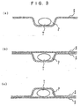
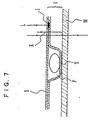
- A sheet wrapping inspecting device which detects a defect including a mingled foreign substance (G2), damage (J1), dirt (H2) of a wrapping sheet (1; 16) and/or a wrapped object, comprising;characterized in that said device is arranged to create a code distribution map from said signals representing said reflection image and said transmission image, wherein the code given to each pixel of said map comprises a binary or multi-value digit expressing the brightness of the corresponding reflection image pixel and comprises a binary or multi-value digit expressing the brightness of the corresponding transmission image pixel,a first light source (3; 14)arranged to illuminate the wrapping sheet (1; 16), said first light source (3; 14) being located above the wrapping sheet (1; 16);a second light source (5, 17) arranged to illuminate the wrapping sheet (1; 16), said second light source (5; 17) being located below the wrapping sheet (1; 16);a sensor arranged to observe the wrapping sheet (1; 16), said sensor being located above or below the wrapping sheet (1; 16) to provide signals representing a two- dimensional a reflection image of the wrapping sheet (1; 16) ; and to provide signals representing a two-dimensional transmission image of the wrapping sheet (1; 16);
and in that said device is arranged to thereafter detect said defect by the help of said code distribution map. - A sheet wrapping inspecting device which detects a defect including a mingled foreign substance (G2), damage (J1), dirt (H2) of a wrapping sheet (1; 16) and/or a wrapped object, comprising:characterized in that said device is arranged to create a color code distribution map from said signal representing said reflection image and said transmission image, wherein the color code given to each pixel of said map comprises binary or multi-value digits expressing color elements according to a color system of the corresponding reflection image pixel and comprises binary or multi-value digits expressing color elements according to a color system of the corresponding transmission image pixel,a first light source (3; 14) arranged to illuminate the wrapping sheet (1; 16), said first light source (3; 14) being located above the wrapping sheet (1; 16);a second light source (5, 17) arranged to illuminate the wrapping sheet (1; 16), said second light source (5; 17) being located below the wrapping sheet (1; 16);a sensor arranged to observe the wrapping sheet (1; 16) said sensor being located above or below the wrapping sheet (1; 16) to provide signals representing a two-dimensional a reflection image of the wrapping sheet (1; 16); and to provide signals representing a two-dimensional transmission image of the wrapping sheet (1; 16);
and in that said device is arranged to thereafter detect said defect by the help of said color code distribution map. - The inspecting device as recited in claim 2, wherein said device inspects a shape and/or color of a wrapped object and/or the wrapping sheet, and detects the defect such as a foreign substance and/or the dirt according to a brightness of the code distribution image obtained from a single or a plurality of color density distributions of the reflected ray image and the transmitted ray image.
- The inspecting device as recited in one of the preceding claims, further comprisingmeans arranged to separate the inputted image inputted from said sensor into an element of the reflected ray image and an element of the transmitted ray image by illuminating said first and second light sources simultaneously to obtain an input image from said two-dimensional sensor.
- The inspecting device as recited in one of the preceding claims, further comprising means arranged to separate the inputted image inputted from said sensor into an element of the reflected ray image and an element of the transmitted ray image by illuminating said first and second light sources simultaneously to obtain an input image from said sensor.
- The inspecting device as recited in claims 2, 3, 4 or 5, wherein at least one of said first and second light sources is equipped with a dimmer or an optical filter which is capable of modifying a quantity of the transmitted ray or a band of transmitted wavelength, whereby said device is capable of adjusting color distributions of the reflected ray and the transmitted ray, or adjusting a ratio of quantity of the reflected ray to quantity of the transmitted ray according to a reflectance, a transmittance and/or a color distribution of the wrapping sheet.
- The inspecting device as recited in claims 2, 3, 4 or 5, wherein said first and/or second light sources are provided with a plurality of light emitting sources of several color peculiarities, and wherein a luminous intensity, a color peculiarity or a wavelength peculiarity are changed or adjusted by controlling electric current of each light emitting source.
- The inspecting device as recited in claims 1, 2, 3, 4 or 5, comprising a reflector which is located under the wrapping sheet and reflects at least five percent (%) of incident light as said second light source.
- The inspecting device as recited in claim 8, wherein said reflector has a reflection specificity depending on a color or a wavelength of the incident light, and wherein the color specificity of said reflector is selected or changed in order to most effectively heighten the color contrast of each part of the color/intensity distribution by enhancing or deducting such distributions.
- The inspecting device as recited in claim 9, wherein said color reflector has a color including a combination of an element of the color to be enhanced and an element of the color to be deducted on a region of a translucent portion of the sheet wrapping on a captured image.
- The inspecting device as recited in claim 9, wherein said color reflector has a color including a combination of a color element to be enhanced and an element of a complementary color to be deducted of a region of a translucent portion of the sheet wrappings on a captured image.
- The inspecting device as recited in claim 8 or 9, wherein said reflector has a concave or convex surface with a diffuser.
- The inspecting device as recited in claim 1, 2, 3, 4, 5, or 8, wherein said at least one of said first and second light sources as recited in claims 1, 2, 3, 4, 5 and 8 and said light source located above the wrapping sheet as recited in claim 8 are located out of a gaze of a camera between the camera and the sheet wrapping in order to reduce an element of a specular reflection from the sheet wrapping.
- The inspecting device as recited in claims 8 or 9, wherein said reflector is located at least 10 mm away from the sheet wrapping.
- The inspecting device as recited in claim 1, 2, 3, 4, or 5, wherein said sensor comprises a one-dimensional line sensor and a driving unit arranged to move said one-dimensional sensor.
- The inspecting device as recited in claim 1, 2, 3, 4 or 5, wherein said sensor comprises a one-dimensional line sensor and a driving unit arranged to move the object to be inspected.
- The inspecting device as recited in one of the preceding claims, wherein, the device further detects a defect by dividing the inputted image into several regions according to the brightness distribution or the code distribution of the inputted image and thereafter giving a code of the neighboring region as an auxiliary code to the code value of each divided region.
- The inspecting device as recited in one of the preceding claims, wherein further a logical operation between images being performed to discriminate a defect based on the logical operation results.
- The inspecting device as recited in claim 4 or 5, said device inspects a shape or color of a wrapped object and/or the sheet and detects the foreign substance and/or the dirt by a computation of a single or a plurality of color distribution images modified from the reflected ray image and the transmitted ray image.
- The inspecting device as recited in claim 4 or 5, wherein said device detects the defect of a wrapped object and the wrapping sheet according to a result of binarization of a color image depending on a brightness distribution, the image being obtained by said sensor under a condition of adjusting a ratio of luminous intensities of both said light sources.
- The inspecting device as recited in claim 4 or 5, wherein said device detects the defect of a wrapped object and the wrapping sheet according to a result of binarization of a grated image depending on a brightness distribution, the image being obtained by said sensor under a condition of adjusting a ratio of luminous intensities of both said light sources.
- The inspecting device as recited in claim 4 or 5, wherein said device detects the defect of a wrapped object and the wrapping sheet according to a result of binarization of a color image depending on a color intensity distribution, the image being obtained by said sensor under a condition of adjusting a ratio of luminous intensities of both said light sources.
Applications Claiming Priority (5)
| Application Number | Priority Date | Filing Date | Title |
|---|---|---|---|
| JP15953297 | 1997-06-17 | ||
| JP15953297A JP3216874B2 (en) | 1997-06-17 | 1997-06-17 | Sheet packaging inspection device and inspection method |
| JP30516897 | 1997-11-07 | ||
| JP30516897A JP3216876B2 (en) | 1997-11-07 | 1997-11-07 | Sheet packaging inspection device |
| PCT/JP1998/002678 WO1998058241A1 (en) | 1997-06-17 | 1998-06-17 | Device for checking sheet packaging |
Publications (3)
| Publication Number | Publication Date |
|---|---|
| EP1003027A1 EP1003027A1 (en) | 2000-05-24 |
| EP1003027A4 EP1003027A4 (en) | 2001-03-21 |
| EP1003027B1 true EP1003027B1 (en) | 2003-08-27 |
Family
ID=26486303
Family Applications (1)
| Application Number | Title | Priority Date | Filing Date |
|---|---|---|---|
| EP98928530A Expired - Lifetime EP1003027B1 (en) | 1997-06-17 | 1998-06-17 | Device for optical sheet wrapping inspection |
Country Status (9)
| Country | Link |
|---|---|
| US (1) | US6445452B1 (en) |
| EP (1) | EP1003027B1 (en) |
| CN (1) | CN1260876A (en) |
| AU (1) | AU8033398A (en) |
| BR (1) | BR9812094A (en) |
| DE (1) | DE69817580T2 (en) |
| IL (1) | IL133522A0 (en) |
| RU (1) | RU2196977C2 (en) |
| WO (1) | WO1998058241A1 (en) |
Families Citing this family (30)
| Publication number | Priority date | Publication date | Assignee | Title |
|---|---|---|---|---|
| AU728792B2 (en) * | 1998-04-17 | 2001-01-18 | Crc For Intelligent Manufacturing Systems & Technologies Ltd | Fault detection apparatus |
| EP1111375B1 (en) * | 1999-12-22 | 2014-12-17 | Novartis AG | Inspection device for packages |
| DE10028239A1 (en) * | 2000-06-07 | 2001-12-13 | Bundesdruckerei Gmbh | Validation of security markings on a document uses a laser to generate an image captured by camera for processing |
| DE60100206T2 (en) * | 2001-08-11 | 2004-02-19 | Agilent Technologies Inc., A Delaware Corp., Palo Alto | Fault indicator for fiber optic connections |
| KR100516828B1 (en) * | 2002-07-29 | 2005-09-26 | 최현호 | method for preventing over-detecting of optical detection and system for performing the same |
| JP5323320B2 (en) * | 2006-07-19 | 2013-10-23 | 有限会社シマテック | Surface inspection device |
| GB2446822A (en) * | 2007-02-23 | 2008-08-27 | Enfis Ltd | Quality control of meat products using optical imaging |
| US7889330B2 (en) | 2008-10-10 | 2011-02-15 | Parata Systems, Llc | Method of taking an image of an object residing in a transparent, colored container |
| US8374965B2 (en) | 2008-11-26 | 2013-02-12 | Parata Systems, Llc | System and method for verifying the contents of a filled, capped pharmaceutical prescription |
| JP5277414B2 (en) * | 2008-12-26 | 2013-08-28 | 株式会社Sumco | Detection device and detection method for colored foreign substances contained in quartz powder raw material |
| RU2411582C2 (en) * | 2009-02-03 | 2011-02-10 | Поль Эмануилович Бланк | Trade system |
| US8345989B1 (en) | 2009-02-16 | 2013-01-01 | Parata Systems, Llc | Illumination station for use in pharmaceutical identification system and methods therefor |
| JP5654486B2 (en) * | 2009-12-11 | 2015-01-14 | 第一実業ビスウィル株式会社 | Appearance inspection device |
| US8477989B2 (en) | 2010-01-14 | 2013-07-02 | Parata Systems, Llc | Method of taking an image of an object residing in a transparent, colored container |
| EP2591761A1 (en) * | 2010-07-09 | 2013-05-15 | Panasonic Corporation | Tablet inspection assistance method and tablet inspection assistance system |
| JP5453350B2 (en) * | 2011-06-23 | 2014-03-26 | 株式会社 システムスクエア | Packaging inspection equipment |
| KR101976163B1 (en) * | 2012-03-08 | 2019-05-31 | 주식회사 셀트라존 | Method and system for code recognition using camera and half mirror on bio device |
| US9699447B2 (en) * | 2012-11-26 | 2017-07-04 | Frito-Lay North America, Inc. | Calibration of a dynamic digital imaging system for detecting defects in production stream |
| CN103698343A (en) * | 2013-12-30 | 2014-04-02 | 上海瑞伯德智能系统科技有限公司 | Pencil nib defect detection device |
| DE102014100699A1 (en) * | 2014-01-22 | 2015-07-23 | Krones Ag | Device for the optical inspection of packaging objects in beverage technology |
| WO2015136598A1 (en) * | 2014-03-10 | 2015-09-17 | 株式会社東芝 | Foreign matter inspection device, foreign matter inspection method, and foreign matter inspection program |
| KR102141216B1 (en) * | 2015-12-16 | 2020-08-04 | 가부시키가이샤 리코 | Inspection system and inspection method |
| US11216936B2 (en) | 2016-02-19 | 2022-01-04 | SCREEN Holdings Co., Ltd. | Defect detection device, defect detection method, and program |
| WO2018150607A1 (en) | 2017-02-20 | 2018-08-23 | Serendipity株式会社 | Appearance inspection device, lighting device, and imaging lighting device |
| JP7019387B2 (en) | 2017-11-17 | 2022-02-15 | キヤノン株式会社 | Image processing equipment, image processing methods, and programs, and image forming equipment |
| CN109001112B (en) * | 2017-12-29 | 2021-01-05 | 北京林业大学 | Light source determination method and system for defect detection |
| CN109883961A (en) * | 2019-03-25 | 2019-06-14 | 深圳市联新移动医疗科技有限公司 | A kind of injection similar drug identification device based on color |
| CN111610197B (en) * | 2020-06-01 | 2023-09-12 | 上海御微半导体技术有限公司 | Defect detection device and defect detection method |
| CN113340920A (en) * | 2021-05-07 | 2021-09-03 | 武汉精测电子集团股份有限公司 | Method and equipment for detecting defects of upper surface and lower surface of transparent material |
| CN114324346A (en) * | 2021-11-12 | 2022-04-12 | 海宁集成电路与先进制造研究院 | Textile flaw detection method and device |
Citations (1)
| Publication number | Priority date | Publication date | Assignee | Title |
|---|---|---|---|---|
| GB2095828A (en) * | 1981-03-31 | 1982-10-06 | Wool Dev Int | Detection of defects in fibrous arrays |
Family Cites Families (13)
| Publication number | Priority date | Publication date | Assignee | Title |
|---|---|---|---|---|
| JPS54143193A (en) * | 1978-04-28 | 1979-11-08 | Fuji Electric Co Ltd | Deffct testing method and apparatus for packaged articles |
| JPS5867093A (en) * | 1981-10-19 | 1983-04-21 | 株式会社東芝 | Method and device for inspecting printed circuit board |
| JPS59147006U (en) * | 1983-03-22 | 1984-10-01 | サンクス株式会社 | Defective product detection device |
| JPS6318568A (en) | 1986-07-11 | 1988-01-26 | Clarion Co Ltd | Cassette loading mechanism |
| US5021645A (en) * | 1989-07-11 | 1991-06-04 | Eaton Corporation | Photoelectric color sensor for article sorting |
| JPH0812053B2 (en) | 1990-04-28 | 1996-02-07 | 正和産業株式会社 | Appearance inspection method and apparatus |
| JPH0776757B2 (en) * | 1990-12-14 | 1995-08-16 | インターナショナル・ビジネス・マシーンズ・コーポレイション | Optical inspection device |
| JP2530532B2 (en) * | 1991-08-22 | 1996-09-04 | シーケーディ株式会社 | Tablet sheet inspection device |
| DE9114260U1 (en) * | 1991-11-15 | 1992-01-23 | Hans P. Friedrich Elektronik Gmbh, 7068 Urbach, De | |
| JP3332543B2 (en) | 1994-01-17 | 2002-10-07 | 三洋電機株式会社 | Tablet inspection system |
| JPH07311160A (en) | 1994-05-19 | 1995-11-28 | Nitto Denko Corp | Method and device for preforming visual inspection |
| JPH0821805A (en) | 1994-07-08 | 1996-01-23 | Datsuku Eng Kk | Appearance inspecting method and device thereof |
| JPH08334469A (en) | 1995-06-09 | 1996-12-17 | Lion Eng Kk | Detector for package such as tablet |
-
1998
- 1998-06-17 US US09/446,010 patent/US6445452B1/en not_active Expired - Fee Related
- 1998-06-17 IL IL13352298A patent/IL133522A0/en unknown
- 1998-06-17 DE DE69817580T patent/DE69817580T2/en not_active Expired - Fee Related
- 1998-06-17 EP EP98928530A patent/EP1003027B1/en not_active Expired - Lifetime
- 1998-06-17 BR BR9812094-8A patent/BR9812094A/en not_active IP Right Cessation
- 1998-06-17 AU AU80333/98A patent/AU8033398A/en not_active Abandoned
- 1998-06-17 WO PCT/JP1998/002678 patent/WO1998058241A1/en active IP Right Grant
- 1998-06-17 RU RU2000101300/28A patent/RU2196977C2/en not_active IP Right Cessation
- 1998-06-17 CN CN98806336.0A patent/CN1260876A/en active Pending
Patent Citations (1)
| Publication number | Priority date | Publication date | Assignee | Title |
|---|---|---|---|---|
| GB2095828A (en) * | 1981-03-31 | 1982-10-06 | Wool Dev Int | Detection of defects in fibrous arrays |
Also Published As
| Publication number | Publication date |
|---|---|
| CN1260876A (en) | 2000-07-19 |
| DE69817580D1 (en) | 2003-10-02 |
| IL133522A0 (en) | 2001-04-30 |
| EP1003027A1 (en) | 2000-05-24 |
| EP1003027A4 (en) | 2001-03-21 |
| AU8033398A (en) | 1999-01-04 |
| US6445452B1 (en) | 2002-09-03 |
| BR9812094A (en) | 2000-07-18 |
| WO1998058241A1 (en) | 1998-12-23 |
| RU2196977C2 (en) | 2003-01-20 |
| DE69817580T2 (en) | 2004-06-24 |
Similar Documents
| Publication | Publication Date | Title |
|---|---|---|
| EP1003027B1 (en) | Device for optical sheet wrapping inspection | |
| US20040150815A1 (en) | Flaw detection in objects and surfaces | |
| US6346966B1 (en) | Image acquisition system for machine vision applications | |
| US6465801B1 (en) | Dust and scratch detection for an image scanner | |
| US7397943B2 (en) | Method and arrangement for touchless detection of data of uneven surfaces | |
| KR102310179B1 (en) | Inspection method using color lighting | |
| JP3216876B2 (en) | Sheet packaging inspection device | |
| CN105431729A (en) | Method and device for observing and analysing optical singularities in glass containers | |
| KR20060053847A (en) | Method for inspecting defects of glass plate and apparatus thereof | |
| CN107667287A (en) | Automatic defect detection and mapping for optical filter | |
| JP2001027612A (en) | Egg inspecting apparatus | |
| JP7223840B2 (en) | Systems, methods, and apparatus for autonomous diagnostic verification of optical components of vision-based inspection systems | |
| CN106940306A (en) | Utilize the contact lenses defects detection of UV illumination | |
| JP3216874B2 (en) | Sheet packaging inspection device and inspection method | |
| JP3090594B2 (en) | Coin discrimination device using image recognition device | |
| WO2019117009A1 (en) | Imaging device for eggs and inspection device for eggs | |
| CN113962238B (en) | Light supplementing light source and identification code scanning device | |
| CN115791831A (en) | Method for detecting defects of irregular reflective surface | |
| US20040081347A1 (en) | Method for determining and evaluating defects in a sample surface | |
| JP2002131239A (en) | Apparatus and method for inspection of foreign body | |
| US20130077851A1 (en) | Three dimensional pattern inspection system | |
| KR102394422B1 (en) | Food surface foreign material inspection optical device using near infrared spectral imaging technology | |
| RU2802531C2 (en) | System and method for detecting glass ceramics | |
| US20230141957A1 (en) | Optical inspection device and inspecting method using the same | |
| US7583377B2 (en) | Optoelectronic process and a device for inspection of an area of revolution of a receptacle |
Legal Events
| Date | Code | Title | Description |
|---|---|---|---|
| PUAI | Public reference made under article 153(3) epc to a published international application that has entered the european phase |
Free format text: ORIGINAL CODE: 0009012 |
|
| 17P | Request for examination filed |
Effective date: 19991213 |
|
| AK | Designated contracting states |
Kind code of ref document: A1 Designated state(s): CH DE ES FI FR GB IT LI SE |
|
| A4 | Supplementary search report drawn up and despatched |
Effective date: 20010205 |
|
| AK | Designated contracting states |
Kind code of ref document: A4 Designated state(s): CH DE ES FI FR GB IT LI SE |
|
| RIC1 | Information provided on ipc code assigned before grant |
Free format text: 7G 01N 21/85 A, 7G 01N 21/95 B |
|
| RAP3 | Party data changed (applicant data changed or rights of an application transferred) |
Owner name: ITO, MINORU Owner name: KONDOU, KIYOYUKI Owner name: YUKI ENGINEERING SYSTEM CO, LTD. |
|
| 17Q | First examination report despatched |
Effective date: 20010710 |
|
| RAP1 | Party data changed (applicant data changed or rights of an application transferred) |
Owner name: YUKI ENGINEERING SYSTEM CO, LTD. |
|
| GRAH | Despatch of communication of intention to grant a patent |
Free format text: ORIGINAL CODE: EPIDOS IGRA |
|
| RTI1 | Title (correction) |
Free format text: DEVICE FOR OPTICAL SHEET WRAPPING INSPECTION |
|
| GRAH | Despatch of communication of intention to grant a patent |
Free format text: ORIGINAL CODE: EPIDOS IGRA |
|
| GRAA | (expected) grant |
Free format text: ORIGINAL CODE: 0009210 |
|
| AK | Designated contracting states |
Designated state(s): CH DE ES FI FR GB IT LI SE |
|
| PG25 | Lapsed in a contracting state [announced via postgrant information from national office to epo] |
Ref country code: IT Free format text: LAPSE BECAUSE OF FAILURE TO SUBMIT A TRANSLATION OF THE DESCRIPTION OR TO PAY THE FEE WITHIN THE PRESCRIBED TIME-LIMIT;WARNING: LAPSES OF ITALIAN PATENTS WITH EFFECTIVE DATE BEFORE 2007 MAY HAVE OCCURRED AT ANY TIME BEFORE 2007. THE CORRECT EFFECTIVE DATE MAY BE DIFFERENT FROM THE ONE RECORDED. Effective date: 20030827 Ref country code: FR Free format text: LAPSE BECAUSE OF FAILURE TO SUBMIT A TRANSLATION OF THE DESCRIPTION OR TO PAY THE FEE WITHIN THE PRESCRIBED TIME-LIMIT Effective date: 20030827 Ref country code: FI Free format text: LAPSE BECAUSE OF FAILURE TO SUBMIT A TRANSLATION OF THE DESCRIPTION OR TO PAY THE FEE WITHIN THE PRESCRIBED TIME-LIMIT Effective date: 20030827 |
|
| REG | Reference to a national code |
Ref country code: GB Ref legal event code: FG4D |
|
| REG | Reference to a national code |
Ref country code: CH Ref legal event code: EP |
|
| REF | Corresponds to: |
Ref document number: 69817580 Country of ref document: DE Date of ref document: 20031002 Kind code of ref document: P |
|
| REG | Reference to a national code |
Ref country code: CH Ref legal event code: NV Representative=s name: NOVAGRAAF INTERNATIONAL SA |
|
| PG25 | Lapsed in a contracting state [announced via postgrant information from national office to epo] |
Ref country code: SE Free format text: LAPSE BECAUSE OF FAILURE TO SUBMIT A TRANSLATION OF THE DESCRIPTION OR TO PAY THE FEE WITHIN THE PRESCRIBED TIME-LIMIT Effective date: 20031127 |
|
| PG25 | Lapsed in a contracting state [announced via postgrant information from national office to epo] |
Ref country code: ES Free format text: LAPSE BECAUSE OF FAILURE TO SUBMIT A TRANSLATION OF THE DESCRIPTION OR TO PAY THE FEE WITHIN THE PRESCRIBED TIME-LIMIT Effective date: 20031208 |
|
| PLBE | No opposition filed within time limit |
Free format text: ORIGINAL CODE: 0009261 |
|
| STAA | Information on the status of an ep patent application or granted ep patent |
Free format text: STATUS: NO OPPOSITION FILED WITHIN TIME LIMIT |
|
| 26N | No opposition filed |
Effective date: 20040528 |
|
| EN | Fr: translation not filed | ||
| PGFP | Annual fee paid to national office [announced via postgrant information from national office to epo] |
Ref country code: GB Payment date: 20060621 Year of fee payment: 9 Ref country code: CH Payment date: 20060621 Year of fee payment: 9 |
|
| PGFP | Annual fee paid to national office [announced via postgrant information from national office to epo] |
Ref country code: DE Payment date: 20060628 Year of fee payment: 9 |
|
| REG | Reference to a national code |
Ref country code: CH Ref legal event code: PL |
|
| GBPC | Gb: european patent ceased through non-payment of renewal fee |
Effective date: 20070617 |
|
| PG25 | Lapsed in a contracting state [announced via postgrant information from national office to epo] |
Ref country code: LI Free format text: LAPSE BECAUSE OF NON-PAYMENT OF DUE FEES Effective date: 20070630 Ref country code: DE Free format text: LAPSE BECAUSE OF NON-PAYMENT OF DUE FEES Effective date: 20080101 Ref country code: CH Free format text: LAPSE BECAUSE OF NON-PAYMENT OF DUE FEES Effective date: 20070630 |
|
| PG25 | Lapsed in a contracting state [announced via postgrant information from national office to epo] |
Ref country code: GB Free format text: LAPSE BECAUSE OF NON-PAYMENT OF DUE FEES Effective date: 20070617 |