EP0998034A2 - Begrenzungsschaltung für einen analogen Verstärker - Google Patents
Begrenzungsschaltung für einen analogen Verstärker Download PDFInfo
- Publication number
- EP0998034A2 EP0998034A2 EP99203532A EP99203532A EP0998034A2 EP 0998034 A2 EP0998034 A2 EP 0998034A2 EP 99203532 A EP99203532 A EP 99203532A EP 99203532 A EP99203532 A EP 99203532A EP 0998034 A2 EP0998034 A2 EP 0998034A2
- Authority
- EP
- European Patent Office
- Prior art keywords
- input
- amplifier
- coupled
- clipping
- circuit
- Prior art date
- Legal status (The legal status is an assumption and is not a legal conclusion. Google has not performed a legal analysis and makes no representation as to the accuracy of the status listed.)
- Granted
Links
Images
Classifications
-
- H—ELECTRICITY
- H03—ELECTRONIC CIRCUITRY
- H03G—CONTROL OF AMPLIFICATION
- H03G11/00—Limiting amplitude; Limiting rate of change of amplitude
Definitions
- This invention generally relates to electronic systems and in particular it relates to analog amplifier clipping circuits.
- Accurate analog clipping control of an amplifier's output nodes is important for applications such as mixed signal codecs.
- Most prior art codecs are a combination of analog input and digital output.
- one type of codec has an analog amplifier providing the analog input to a sigma-delta analog to digital (A/D) converter.
- A/D analog to digital
- the A/D converter and a corresponding digital filter can overload.
- the digital filter overloads internal clipping mechanisms prevent wrap around of the digital signal. This creates a digital representation of a trapezoidal signal that contains harmonics with sufficient power to increase the FM modulation depth to undesirable levels.
- the analog clipping circuit includes: a main amplifier; a feedback resistor coupled between a first input of the main amplifier and an output of the main amplifier; a first current source coupled in parallel with the feedback resistor; a first clipping amplifier coupled to the first current source for controlling the first current source, the first clipping amplifier having a first input coupled to an output of the main amplifier and a second input coupled to a first reference node; a second current source coupled in parallel with the feedback resistor; and a second clipping amplifier coupled to the second current source for controlling the second current source, the second clipping amplifier having a first input coupled to an output of the main amplifier and a second input coupled to a reference node.
- the preferred embodiment circuits are designed to limit the output voltage swings of either a fully differential or single ended amplifier gain cell.
- the circuits employ an analog negative feedback loop to control the current through the main amplifier feedback resistor.
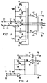
- a preferred embodiment analog amplifier clipping circuit is shown in Figure 1.
- the circuit of Figure 1 is a fully differential circuit, but the circuit can also be implemented as a single ended circuit.
- the circuit of Figure 1 includes amplifier 20, resistors 22, 24, 26, and 28, positive input node 34, negative input node 36, positive output node 38, negative output node 40, feedback amplifiers 42 and 44, and low clip voltage nodes 46 and 48, and transistors 50, 52, 54, and 56. Both clipping amplifiers 42 and 44 have P-channel input stages, as does the main amplifier 20.
- the transistors 50, 52, 54, and 56 serve as current sources that are controlled by the output voltages from feedback amplifiers 42 and 44. As either output voltage V out- or output voltage V out+ reaches the low clip voltage V cl , the transistors 50, 52, 54, and 56 divert any additional current so that the current I f can remain constant, thus keeping output voltage V out+ or V out- at the clipping level V cl .
- clipping amplifier 42 When output voltage V out+ is greater than clipping voltage V cl , clipping amplifier 42 has its minus input terminal larger than its positive input terminal. This causes the output voltage V A of amplifier 42 to be a low voltage (A 1 *(V cl - V out+ ) where A 1 is the gain of amplifier 42). While the output voltage V A of amplifier 42 is at a low voltage, transistors 50 and 52 remain off, keeping the normal operation of the circuit unchanged.
- V out+ and V out- are inverse of each other
- the output V B of amplifier 44 is also a low voltage during normal operation, and transistors 54 and 56 are off. Normal operation is defined by the peak voltage swing of ⁇ V mid -V out+ ⁇ and ⁇ V mid - V out- ⁇ is less than ⁇ V mid - V cl ⁇ , where V mid is the supply voltage divided by two.
- the voltage at node 70 does not move due to the feedback.
- current I swA must increase.
- the feedback loop dynamically varies current I swA to keep voltage V out+ approximately equal to clipping voltage V cl .
- V cm V mid .
- V cm is the common-mode voltage.
- the transistor 52 will also turn on in this cycle. This helps to keep the input common-mode V 70 constant.
- the current equations for node 71 are shown below.
- V out- is constant, V in+ is getting smaller, I swB is getting larger so that V 70 can remain constant. Due to the polarity of the transistors 50 and 52, and signal swings involved, current I swB is less than current I swA , therefore voltage V 70 will get smaller by some amount. This is tolerable for large gain variations, R f /R i , because amplifier 20 is a P-channel input pair type amp.
- the width to length ratio of transistor 50 is equal to the width to length ratio of transistor 52.
- the width to length ratio of transistor 52 can be made greater than the width to length ratio of transistor 50 to increase the current through transistor 52 for a given control voltage V A . This will hold the input common-mode level even closer to the ideal case. Without transistor 52, this scheme will stop working when the voltage at node 70 drops so low that the common-mode feedback circuit of amplifier 20 stops working.
- a single-ended version of the analog clipping circuit is shown in Figure 2.
- the circuit of Figure 2 includes amplifier 80, resistors 82 and 84, input node 86, V mid node 88, output node 90, feedback amplifiers 92 and 94, low clip voltage node 96, high clip voltage node 98, and transistors 100 and 102.
- the single-ended circuit of Figure 2 operates by the same general theory of the differential circuit of Figure 1 with some differences in the implementation.
- the differential circuit of Figure 1 relies on the symmetrical natures of V out+ and V out- . When V out+ is clipping low, V out- must be clipping high. Therefore, only the low reference clipping voltage is used.
- the signal is a complex single-ended waveform that needs two clipping reference voltages, a high clip voltage V ch and a low clip voltage V cl .
- one clipping amp 92 Since there is a V ch reference, one clipping amp 92 must be an N-channel input stage and the other clipping amp 94 will remain a P-channel input stage.
- amplifier 80 has one input terminal 88 tied to voltage V mid .
- the gain of amplifier 80 and its feedback force the voltage on the other input terminal 89 to be V mid as well.
- one feedback switch is a PMOS transistor 100 and the other an NMOS transistor 102.
- R i is resistor 82.
- R f is resistor 84.
- I 102 is the current through transistor 102.
- I 100 is the current through transistor 100.
- N-channel transistor 102 and P-channel transistor 100 act like voltage controlled current sources in a feedback loop to keep the current in resistor 84 constant, thus keeping V out constant (clipped to either V ch or V cl ).
Landscapes
- Tone Control, Compression And Expansion, Limiting Amplitude (AREA)
- Amplifiers (AREA)
Applications Claiming Priority (2)
| Application Number | Priority Date | Filing Date | Title |
|---|---|---|---|
| US10650298P | 1998-10-30 | 1998-10-30 | |
| US106502 | 1998-10-30 |
Publications (3)
| Publication Number | Publication Date |
|---|---|
| EP0998034A2 true EP0998034A2 (de) | 2000-05-03 |
| EP0998034A3 EP0998034A3 (de) | 2001-02-07 |
| EP0998034B1 EP0998034B1 (de) | 2004-06-30 |
Family
ID=22311756
Family Applications (1)
| Application Number | Title | Priority Date | Filing Date |
|---|---|---|---|
| EP99203532A Expired - Lifetime EP0998034B1 (de) | 1998-10-30 | 1999-10-27 | Begrenzungsschaltung für einen analogen Verstärker |
Country Status (4)
| Country | Link |
|---|---|
| US (1) | US6084467A (de) |
| EP (1) | EP0998034B1 (de) |
| AT (1) | ATE270469T1 (de) |
| DE (1) | DE69918394T2 (de) |
Families Citing this family (10)
| Publication number | Priority date | Publication date | Assignee | Title |
|---|---|---|---|---|
| US6229470B1 (en) * | 1998-07-28 | 2001-05-08 | Texas Instruments Incorporated | Analog clipping circuit for mixed signal codecs |
| WO2000038316A1 (en) * | 1998-12-22 | 2000-06-29 | Koninklijke Philips Electronics N.V. | Computer tomograph with a multi-stage charge-integrated read amplifier |
| US6424280B2 (en) * | 2000-01-21 | 2002-07-23 | Texas Instruments Incorporated | Signal clipping circuit for switched capacitor sigma delta analog to digital converters |
| US6882861B2 (en) * | 2001-04-30 | 2005-04-19 | Texas Instruments Incorporated | Wireless user terminal and system having signal clipping circuit for switched capacitor sigma delta analog to digital converters |
| TW564592B (en) * | 2002-03-22 | 2003-12-01 | Wistron Corp | Amplification circuit for restricting output signal amplitude supplied to a speaker |
| US7110726B1 (en) * | 2003-05-22 | 2006-09-19 | Quake Global, Inc. | RF ASIC for subscriber communicator |
| US7053807B1 (en) | 2005-03-03 | 2006-05-30 | Analog Devices, Inc. | Apparatus and method for controlling the state variable of an integrator stage in a modulator |
| TWI390840B (zh) * | 2008-11-12 | 2013-03-21 | Realtek Semiconductor Corp | 具有自動調整輸出阻抗功能之線驅動器 |
| US10164595B2 (en) | 2013-08-14 | 2018-12-25 | The Governors Of The University Of Alberta | Clipped amplifier |
| CN112260667A (zh) * | 2020-11-09 | 2021-01-22 | 苏州坤元微电子有限公司 | 单限幅电路及双限幅电路 |
Family Cites Families (8)
| Publication number | Priority date | Publication date | Assignee | Title |
|---|---|---|---|---|
| DE2436638A1 (de) * | 1974-07-26 | 1976-02-05 | Licentia Gmbh | Geregelte begrenzung der ausgangsspannung von regelverstaerkern |
| US3999084A (en) * | 1975-07-24 | 1976-12-21 | Gte Laboratories Incorporated | Limiting amplifier with adjustable limits |
| US4070632A (en) * | 1976-09-22 | 1978-01-24 | Tuttle John R | Discrete-gain output limiter |
| US4849708A (en) * | 1988-06-30 | 1989-07-18 | Advanced Miere Devices, Inc. | Fully differential non-linear amplifier |
| US5175508A (en) * | 1991-12-05 | 1992-12-29 | Ford Motor Company | Voltage-controlled amplifier using operational amplifier |
| US5412346A (en) * | 1993-12-13 | 1995-05-02 | At&T Corp. | Variable gain voltage signal amplifier |
| DE19643198A1 (de) * | 1996-10-19 | 1998-04-23 | Adolf Wuerth Gmbh & Co Kg | Bolzenschubgerät |
| EP0838914A3 (de) * | 1996-10-25 | 2002-03-27 | Nec Corporation | Schaltungsanordnung zur Verstärkung eines elektrischen Signals aus einem optischen Signal umgewandelt |
-
1999
- 1999-10-07 US US09/414,409 patent/US6084467A/en not_active Expired - Lifetime
- 1999-10-27 DE DE69918394T patent/DE69918394T2/de not_active Expired - Lifetime
- 1999-10-27 EP EP99203532A patent/EP0998034B1/de not_active Expired - Lifetime
- 1999-10-27 AT AT99203532T patent/ATE270469T1/de not_active IP Right Cessation
Also Published As
| Publication number | Publication date |
|---|---|
| EP0998034B1 (de) | 2004-06-30 |
| EP0998034A3 (de) | 2001-02-07 |
| DE69918394D1 (de) | 2004-08-05 |
| ATE270469T1 (de) | 2004-07-15 |
| DE69918394T2 (de) | 2005-08-04 |
| US6084467A (en) | 2000-07-04 |
Similar Documents
| Publication | Publication Date | Title |
|---|---|---|
| EP0766381B1 (de) | Verbesserter Eintakt/Differenzumsetzer mit beschränktem Gleichtakteingangssignalbedarf | |
| KR20000052438A (ko) | 동적 보상 증폭기 및 그 방법 | |
| KR970063901A (ko) | 연산증폭회로 | |
| EP0594305A1 (de) | Vergleichsschaltung | |
| JP3181507B2 (ja) | スイッチドキャパシタを導入した低電圧差動増幅器のための装置 | |
| EP0998034B1 (de) | Begrenzungsschaltung für einen analogen Verstärker | |
| KR100311447B1 (ko) | 서로 무관한 게인 및 바이어싱을 갖는 가변 게인 전류 합산 회로 | |
| US6236195B1 (en) | Voltage variation correction circuit | |
| US5057789A (en) | Class AB CMOS amplifier | |
| US4533877A (en) | Telecommunication operational amplifier | |
| JP3134846B2 (ja) | ヒステリシスコンパレータ回路 | |
| US6975100B2 (en) | Circuit arrangement for regulating the duty cycle of electrical signal | |
| US10236851B2 (en) | Wide bandwidth variable gain amplifier and exponential function generator | |
| US6777984B2 (en) | Differential amplifying method and apparatus capable of responding to a wide input voltage range | |
| JPH0269007A (ja) | 差動増幅器 | |
| US6333673B2 (en) | Electronic circuit | |
| KR100309028B1 (ko) | 제조 방법 및 동작 상태의 변화로 인한 동작 변화를 dc바이어싱의 변화를 트래킹해서 트랙하는 게인 제어 신호 발생기 | |
| EP1429456A1 (de) | Regelverstärker mit niedrigem stromverbrauch | |
| US6650184B2 (en) | High gain amplifier circuits and their applications | |
| US6559716B2 (en) | Switchable operational amplifier for switched op-amp applications | |
| JPH09219629A (ja) | 演算増幅器 | |
| US4956613A (en) | Differential amplifier having externally controllable power consumption | |
| KR100821122B1 (ko) | 씨모스형 가변이득 증폭 장치 | |
| JPS60217709A (ja) | 演算増幅回路 | |
| JPS61131606A (ja) | 差動増幅回路 |
Legal Events
| Date | Code | Title | Description |
|---|---|---|---|
| PUAI | Public reference made under article 153(3) epc to a published international application that has entered the european phase |
Free format text: ORIGINAL CODE: 0009012 |
|
| AK | Designated contracting states |
Kind code of ref document: A2 Designated state(s): AT BE CH CY DE DK ES FI FR GB GR IE IT LI LU MC NL PT SE |
|
| AX | Request for extension of the european patent |
Free format text: AL;LT;LV;MK;RO;SI |
|
| PUAL | Search report despatched |
Free format text: ORIGINAL CODE: 0009013 |
|
| AK | Designated contracting states |
Kind code of ref document: A3 Designated state(s): AT BE CH CY DE DK ES FI FR GB GR IE IT LI LU MC NL PT SE |
|
| AX | Request for extension of the european patent |
Free format text: AL;LT;LV;MK;RO;SI |
|
| 17P | Request for examination filed |
Effective date: 20010807 |
|
| AKX | Designation fees paid |
Free format text: AT BE CH CY DE DK ES FI FR GB GR IE IT LI LU MC NL PT SE |
|
| GRAP | Despatch of communication of intention to grant a patent |
Free format text: ORIGINAL CODE: EPIDOSNIGR1 |
|
| GRAS | Grant fee paid |
Free format text: ORIGINAL CODE: EPIDOSNIGR3 |
|
| GRAA | (expected) grant |
Free format text: ORIGINAL CODE: 0009210 |
|
| AK | Designated contracting states |
Kind code of ref document: B1 Designated state(s): AT BE CH CY DE DK ES FI FR GB GR IE IT LI LU MC NL PT SE |
|
| PG25 | Lapsed in a contracting state [announced via postgrant information from national office to epo] |
Ref country code: NL Free format text: LAPSE BECAUSE OF FAILURE TO SUBMIT A TRANSLATION OF THE DESCRIPTION OR TO PAY THE FEE WITHIN THE PRESCRIBED TIME-LIMIT Effective date: 20040630 Ref country code: LI Free format text: LAPSE BECAUSE OF FAILURE TO SUBMIT A TRANSLATION OF THE DESCRIPTION OR TO PAY THE FEE WITHIN THE PRESCRIBED TIME-LIMIT Effective date: 20040630 Ref country code: IT Free format text: LAPSE BECAUSE OF FAILURE TO SUBMIT A TRANSLATION OF THE DESCRIPTION OR TO PAY THE FEE WITHIN THE PRESCRIBED TIME-LIMIT;WARNING: LAPSES OF ITALIAN PATENTS WITH EFFECTIVE DATE BEFORE 2007 MAY HAVE OCCURRED AT ANY TIME BEFORE 2007. THE CORRECT EFFECTIVE DATE MAY BE DIFFERENT FROM THE ONE RECORDED. Effective date: 20040630 Ref country code: FI Free format text: LAPSE BECAUSE OF FAILURE TO SUBMIT A TRANSLATION OF THE DESCRIPTION OR TO PAY THE FEE WITHIN THE PRESCRIBED TIME-LIMIT Effective date: 20040630 Ref country code: CY Free format text: LAPSE BECAUSE OF FAILURE TO SUBMIT A TRANSLATION OF THE DESCRIPTION OR TO PAY THE FEE WITHIN THE PRESCRIBED TIME-LIMIT Effective date: 20040630 Ref country code: CH Free format text: LAPSE BECAUSE OF FAILURE TO SUBMIT A TRANSLATION OF THE DESCRIPTION OR TO PAY THE FEE WITHIN THE PRESCRIBED TIME-LIMIT Effective date: 20040630 Ref country code: BE Free format text: LAPSE BECAUSE OF FAILURE TO SUBMIT A TRANSLATION OF THE DESCRIPTION OR TO PAY THE FEE WITHIN THE PRESCRIBED TIME-LIMIT Effective date: 20040630 Ref country code: AT Free format text: LAPSE BECAUSE OF FAILURE TO SUBMIT A TRANSLATION OF THE DESCRIPTION OR TO PAY THE FEE WITHIN THE PRESCRIBED TIME-LIMIT Effective date: 20040630 |
|
| REG | Reference to a national code |
Ref country code: GB Ref legal event code: FG4D Ref country code: CH Ref legal event code: EP |
|
| REG | Reference to a national code |
Ref country code: IE Ref legal event code: FG4D |
|
| REF | Corresponds to: |
Ref document number: 69918394 Country of ref document: DE Date of ref document: 20040805 Kind code of ref document: P |
|
| PG25 | Lapsed in a contracting state [announced via postgrant information from national office to epo] |
Ref country code: SE Free format text: LAPSE BECAUSE OF FAILURE TO SUBMIT A TRANSLATION OF THE DESCRIPTION OR TO PAY THE FEE WITHIN THE PRESCRIBED TIME-LIMIT Effective date: 20040930 Ref country code: GR Free format text: LAPSE BECAUSE OF FAILURE TO SUBMIT A TRANSLATION OF THE DESCRIPTION OR TO PAY THE FEE WITHIN THE PRESCRIBED TIME-LIMIT Effective date: 20040930 Ref country code: DK Free format text: LAPSE BECAUSE OF FAILURE TO SUBMIT A TRANSLATION OF THE DESCRIPTION OR TO PAY THE FEE WITHIN THE PRESCRIBED TIME-LIMIT Effective date: 20040930 |
|
| PG25 | Lapsed in a contracting state [announced via postgrant information from national office to epo] |
Ref country code: ES Free format text: LAPSE BECAUSE OF FAILURE TO SUBMIT A TRANSLATION OF THE DESCRIPTION OR TO PAY THE FEE WITHIN THE PRESCRIBED TIME-LIMIT Effective date: 20041011 |
|
| PG25 | Lapsed in a contracting state [announced via postgrant information from national office to epo] |
Ref country code: LU Free format text: LAPSE BECAUSE OF NON-PAYMENT OF DUE FEES Effective date: 20041027 Ref country code: IE Free format text: LAPSE BECAUSE OF NON-PAYMENT OF DUE FEES Effective date: 20041027 |
|
| PG25 | Lapsed in a contracting state [announced via postgrant information from national office to epo] |
Ref country code: MC Free format text: LAPSE BECAUSE OF NON-PAYMENT OF DUE FEES Effective date: 20041031 |
|
| NLV1 | Nl: lapsed or annulled due to failure to fulfill the requirements of art. 29p and 29m of the patents act | ||
| REG | Reference to a national code |
Ref country code: CH Ref legal event code: PL |
|
| ET | Fr: translation filed | ||
| PLBE | No opposition filed within time limit |
Free format text: ORIGINAL CODE: 0009261 |
|
| STAA | Information on the status of an ep patent application or granted ep patent |
Free format text: STATUS: NO OPPOSITION FILED WITHIN TIME LIMIT |
|
| 26N | No opposition filed |
Effective date: 20050331 |
|
| REG | Reference to a national code |
Ref country code: IE Ref legal event code: MM4A |
|
| PG25 | Lapsed in a contracting state [announced via postgrant information from national office to epo] |
Ref country code: PT Free format text: LAPSE BECAUSE OF NON-PAYMENT OF DUE FEES Effective date: 20041130 |
|
| PGFP | Annual fee paid to national office [announced via postgrant information from national office to epo] |
Ref country code: GB Payment date: 20140925 Year of fee payment: 16 |
|
| PGFP | Annual fee paid to national office [announced via postgrant information from national office to epo] |
Ref country code: FR Payment date: 20140924 Year of fee payment: 16 Ref country code: DE Payment date: 20141028 Year of fee payment: 16 |
|
| REG | Reference to a national code |
Ref country code: DE Ref legal event code: R119 Ref document number: 69918394 Country of ref document: DE |
|
| GBPC | Gb: european patent ceased through non-payment of renewal fee |
Effective date: 20151027 |
|
| PG25 | Lapsed in a contracting state [announced via postgrant information from national office to epo] |
Ref country code: DE Free format text: LAPSE BECAUSE OF NON-PAYMENT OF DUE FEES Effective date: 20160503 Ref country code: GB Free format text: LAPSE BECAUSE OF NON-PAYMENT OF DUE FEES Effective date: 20151027 |
|
| REG | Reference to a national code |
Ref country code: FR Ref legal event code: ST Effective date: 20160630 |
|
| PG25 | Lapsed in a contracting state [announced via postgrant information from national office to epo] |
Ref country code: FR Free format text: LAPSE BECAUSE OF NON-PAYMENT OF DUE FEES Effective date: 20151102 |