EP0997859A2 - Lichtschrankensteuergerät - Google Patents
Lichtschrankensteuergerät Download PDFInfo
- Publication number
- EP0997859A2 EP0997859A2 EP99121290A EP99121290A EP0997859A2 EP 0997859 A2 EP0997859 A2 EP 0997859A2 EP 99121290 A EP99121290 A EP 99121290A EP 99121290 A EP99121290 A EP 99121290A EP 0997859 A2 EP0997859 A2 EP 0997859A2
- Authority
- EP
- European Patent Office
- Prior art keywords
- rom
- light barrier
- output
- control device
- outputs
- Prior art date
- Legal status (The legal status is an assumption and is not a legal conclusion. Google has not performed a legal analysis and makes no representation as to the accuracy of the status listed.)
- Withdrawn
Links
Images

Classifications
-
- G—PHYSICS
- G01—MEASURING; TESTING
- G01V—GEOPHYSICS; GRAVITATIONAL MEASUREMENTS; DETECTING MASSES OR OBJECTS; TAGS
- G01V8/00—Prospecting or detecting by optical means
- G01V8/10—Detecting, e.g. by using light barriers
- G01V8/20—Detecting, e.g. by using light barriers using multiple transmitters or receivers
-
- H—ELECTRICITY
- H03—ELECTRONIC CIRCUITRY
- H03K—PULSE TECHNIQUE
- H03K2217/00—Indexing scheme related to electronic switching or gating, i.e. not by contact-making or -breaking covered by H03K17/00
- H03K2217/94—Indexing scheme related to electronic switching or gating, i.e. not by contact-making or -breaking covered by H03K17/00 characterised by the way in which the control signal is generated
- H03K2217/941—Indexing scheme related to electronic switching or gating, i.e. not by contact-making or -breaking covered by H03K17/00 characterised by the way in which the control signal is generated using an optical detector
- H03K2217/94114—Optical multi axis
Definitions
- the invention relates to a light barrier control device for several light barriers, each with a light transmitter and have a light receiver.
- the control unit controls the light transmitter, asks the signals of the light receiver and generates a safety signal, if at least a light barrier is interrupted.
- Light barrier control units are used primarily in mechanical engineering widely used to avoid dangers from accidental Penetration of parts of the operator's body or also objects in risk zones within the To avoid machine. Usually is one Photoelectric barrier not sufficient, but the risk zone is protected with a number of light barriers that are often combined into light curtains, which are made of there are many stacked light barriers. That generated by an electronic unit of the control unit Safety signal is mostly used to actuate a Contactor that stops the machine. However, it can also serve to control other safety functions, for example to switch on an acoustic Warning signal or automatic blocking of the risk zone.
- the Electronic unit of the control unit which the photoelectric sensors controls and a safety signal from the receiver signals generated, therefore usually contains one Variety of verification functions with which the items the light barriers as well as the electronics unit be continuously checked for correct function.
- Microcomputers are usually used for this purpose the various functions using complex programs monitor the safety device (DE 3790010 T1). Risks from errors in the microcomputers themselves can only be eliminated in that at least two independent microcomputers are used who check each other.
- Such a light barrier control device is from the EP 0371317 A2 known. It is characterized in that a high security standard with little construction effort is achieved. To avoid internal errors in the Components of the ROM step switch caused risks to be largely excluded in the pre-publication suggested every light barrier receiver to be connected in parallel to two inputs of the ROM and one To use part of the outputs of the ROM as control outputs which belong to the return outputs. It is the memory content of the ROM with respect to the control outputs chosen so that all N-bit words are at the feedback inputs each in at least two bits from each other differentiate.
- the object of a light barrier control device to provide that with no significant increase the constructional effort, the control and query allows a larger number of light barriers.
- the task is with a light barrier control unit ROM step switch of the type explained above thereby solved that the electronic unit has two ROM step switches each with a ROM and a subordinate Step memory contains, each ROM receiver inputs has to which receiver signals are present that two ROM stepping mechanisms are clocked synchronously and the useful signal outputs of both stepping switches a common security signal generating device are connected, which generates a safety signal when at the useful signal output of at least one of the Stepper switch generates an accident output signal becomes.
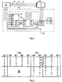
- Figures 1 and 2 serve the principle of a light barrier control device with an electronic unit Basis of a ROM step switch based on a simple one To explain example.
- a transmitter unit 1 sends four light beams 2 to 5 a receiver unit 6.
- the transmitter unit contains four light transmitters and the receiver unit four Receiver with associated electronic circuit.
- the four light barriers 2 to 5 can, for example, one Light curtain to secure a risk zone in a Form the machine.
- the electronics unit 15 of a control unit comprises a total of 8 ROM stepping mechanism, a decoder 9 and a security signal generating device 10.
- the ROM step switch exists from a ROM 11, one according to its function as Step memory designated memory module 12 with several bistable memory elements (flip-flops) and one Clock generator 13.
- the ROM 11 contains a variety of storage locations can be controlled via addressing inputs B0 to B5.
- the memory content of the memory location controlled in each case is present at the outputs R0 to R2.
- the ROM 11 with the help of a standard EPROM chip realized inexpensively.
- the outputs R0 to R2 of the ROM 11 are with corresponding Inputs I0 to I2 of the step memory 12 connected.
- On the outputs X0 to X2 of the step memory are available after a clock of the clock generator 13 which before Clock at the digital states present at its inputs on.
- Part N of the outputs of the step memory 12 is attributed to inputs B4, B5 of the ROM.
- the entrances B4, B5 and I1, I2 or the outputs R1, R2 and X1, X2 are used as return inputs or return outputs of the corresponding components.
- the feedback outputs X1, X2 of the step memory 12 are also connected to the decoder 9, which from the drive signals applied to its inputs generated for the transmitter unit 1. Alternatively, you can also outputs independent of the feedback inputs of the ROM step switch 8 for controlling the Photoelectric sensors can be used.
- the ROM 11 also has a useful signal output R0 on that with a useful signal input I0 of the step memory 12 is connected.
- the assigned useful signal output X0 is with the safety signal generating device 10 connected.
- the outputs of the four combined in the receiver unit 6 Light receivers are at inputs B0 to B3 of the ROM 11 connected.
- the respective memory address of the ROM 11 accordingly comprises a first partial address TA1 ( Figure 2) by the output signals of the feedback outputs X1, X2 of the step memory 12 are formed and a second partial address TA2, which consists of the output signals the receiver of light barriers 2 to 5 consists.
- the sequence of steps and the control of the light transmitter Light barriers LS in the normal operating cycle is controlled by the N-bit words present at the feedback outputs R1, R2 determined that repeat themselves cyclically.
- the N-bit words present at the feedback outputs R1, R2 determined that repeat themselves cyclically.
- there are the four possible states of one 2-bit word i.e. the number of controlled light barriers corresponds to the maximum possible number of different States at the feedback outputs.
- each Case is the condition of a cyclically repeating Bit pattern to understand that none at the feedback inputs in the normal operating cycle of the bit pattern pending occurs twice and that in each case that applied to the feedback outputs Bit pattern that first partial address TA1 of next step that forms together with a second partial address TA2, which is an undisturbed state corresponds to the respectively controlled light barrier, the one Memory location of the ROM addressed in which the next first partial address of the fixed normal operating cycle is saved.
- the second partial address TA2 contains for the controlled light barrier is a logical one and for the other light barriers a zero.
- the connected thereby controlled with the respective first partial address Storage locations contain the first partial address of the next step.
- the output signals are correct of columns R1 and R2 with the next row of Input signals of columns B4 and B5 match.
- the ROM stepper goes through in the normal operating cycle constantly the one in Figure 2 in the first four Lines represented states (steps) with each Clock of the clock generator 13 a switch to the next Line is done.
- the transmitters of transmitter unit 1 are thus cyclically controlled.
- the cyclic loop will not interrupted as long as the light barriers are free.
- R0 contained in the shown Example all four controlled storage locations of the ROM a logical one (hereinafter also with Denoted "H" (high), i.e. the normal operation output sequence is formed from a sequence of H states.
- This normal operation output sequence can be used for the Those skilled in the art (for example, as in the EP 0 371 317, with the aid of a frequency-selective output transformer) into an output signal of the electronic unit 15 are implemented, the normal operation of the connected machine controls. It is hereinafter referred to as Normal operating signal of the electronics unit.
- a relay can be activated via the the machine monitored by the light barriers with electricity is supplied.
- the ROM For each bit pattern that deviates from the normal operating cycle (labeled B in Fig. 2) at inputs B0 to B5, the ROM contains a memory content to which the Safety signal generating device 10, (for example with the help of an appropriate decoder circuit) responds in that it emits a safety signal. Such a bit pattern is called an accident output signal of the step switch. In the illustrated In this case, it is determined by the useful signal output R0. It contains for all storage locations that are not of that Normal operating cycle can be controlled, a logical Zero by the security signal generating device into a corresponding safety signal from the electronics unit is converted.
- FIGS. 1 and 2 ROM step switch corresponds to the state of the art according to EP 0 371 317 A1.
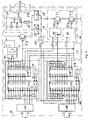
- Figure 3 Electronics unit 15 of a control device according to the invention in that there are two ROM stepping devices 8A and 8B each with a ROM 11A and 11B and one each Has step memory 12A and 12B.
- the query of the Photoelectric barriers are carried out by both step switches.
- Another ingredient the transmitter control is output Q6 of the stepper 8A, which has a switching amplifier element, such as the switching transistor T3 shown the power supply to the transmitter unit controls the Enable transmitter activation explained below.
- Both stepping gears are shared by one Clock generator 13 clocked. It generates both (in particular when switching on the device) Reset signals for the Reset inputs MR of the two step memories 12A and 12B as well as a clock that is connected to the clock inputs CLK Step memory 12A and 12B is created. Besides, will the clock generator, the signal S of the output Q6 of the Step switch 8A supplied.
- the ROM modules are 32 K x 8 EPROM with 15 inputs and 8 outputs.
- the step memory blocks 12 are 8 x D flip flops. The comparison to Figure 1 allows a larger number of outputs the independent control and query of a larger one Number of light barriers, in the case shown with the three outputs Q0 to Q2 eight light barriers independently can be controlled.
- ROMs 11A and 11B are each seven, namely the outputs V0 to V6, feedback outputs, to corresponding feedback inputs D0 to D6 the step memory 12A, 12B are connected. Consequently their bit patterns are in the next step at the corresponding inputs, namely the inputs A0 to A6 of the ROM. The only one not returned
- the ROM output is the useful signal output V7, whose Output signal after the next clock on the Useful signal output Q7 of the step memory 12A and 12B is present.
- the outputs Q7 of the step memories 12A and 12B form the outputs of the step switch 8A and 8B, whose Signals of the safety signal generating device 10 are supplied.
- each case four inputs A7 to A10 of the two ROMs 11A and 11B serve as receiver inputs, to which the signals of the receiver unit 6 are applied, the signals of the receivers not being supplied directly but rather indirectly via an encoder 16A or 16B in the case shown.
- the number of queried receivers can be greater than the number of available inputs.
- the four inputs 2 enable 4 digital states, so that 8 light barrier receivers (each with two possible states) can be queried independently.
- each of the ROMs 11A and 11B has a feedback input A11, on which one from the security signal generating device 10 feedback signal led out RM is applied to during the normal operating cycle a check of the switching transistors contained therein T1, T2 to allow for short circuit as below is explained.
- the two step mechanisms 8A and 8B are synchronized clocked. Because only one of the stepping switches controls the light barriers, but the receiver signals are fed to both stepping switches, each leads Deviation from the synchronous run to generate a Security signals.
- each ROM 11A and 11B one Input A12 on that with the useful signal output Q7 of the other Step switch is connected so that the output signal AT1 of the step switch 8A at the input A12 of the ROM 11B and vice versa the output signal AT2 of the Step switch 8B is present at the input A12 of the ROM 11A. Since the inputs A12 serve the function of the to monitor each other (partner) step switch, they are referred to as partner monitoring inputs.
- each ROM has setting inputs A13 and A14 on, to the individually adjustable switches (for example DIP switches) 17A and 17B are connected to the setting of various operating states of the To allow control unit, which is in terms of Differentiate between the number of light barriers.
- individually adjustable switches for example DIP switches
- the output signals AT1 and AT2 are each monostable Multivibrator (monoflop) fed by Edges of the digital states is triggered and on the each output 26a and 27a generates a pulse, its duration the duration of the respective monoflop corresponds.
- the output signals of the monoflops 26 and 27 are at the input of a switching transistor T1 or T2 on.
- Switching elements e.g. Darlington or MOS transistors
- the two switching transistors T1 and T2 are connected in series, so that current flows through the series circuit is only possible if both transistors are conductive.
- the transistors T1 and T2 (or other switching elements) thus form (preferably, as shown, in connection with upstream monoflops) a logic circuit 19, through which the two output signals of Step switches 8A and 8B in the sense of a logical "and" link are linked in such a way that a Output signal, which is working and free Photoelectric sensors correspond to (normal operating signal), only generated can be if both stepping switches 8A and 8B generate a normal operating output sequence. Otherwise a security signal is given.
- the output signal the logic circuit 19 is via a Schmitt trigger 29 to the feedback inputs A11 of the ROM 11A and 11B connected.
- the control unit contains a relay unit 20. It exists in the case shown, from two positively driven Relays, the components of which are marked with the letters a and b are.
- the relay coils 21a and 21b are connected in parallel and actuate the make contacts 22a, 23a and 24a or 22b, 23b and 24b.
- By the illustrated equivalent circuit of the contacts 22a, 23a, 22b, 23b in the power supply of the relay coils 21a and 21b is achieved that in the event of getting caught one of the relays the other gets no voltage and therefore a malfunction due to one Getting caught is prevented.
- This design of the Relay unit 20 is particularly advantageous, however, can also other known relay units from the logic circuit 19 can be controlled.
- the output 28 of the control unit is shown in the Embodiment of the working contacts 24a and 24b relays a and b are formed. At the exit 28 is in usually connected a successor circuit, the usually a motor contactor from the light barrier control unit protected machine. Besides takes over the subsequent circuit in the usual way Functions (start and restart interlock; start test). A more detailed description is not necessary, since these elements of the light barrier control device according to the invention in the same way as conventional ones Photoelectric control units can be controlled.
- a fuse 25 is in the case shown in the relay unit 20 arranged. You can also use another Place in the one switched by transistors T1 and T2 Current path may be provided. Transistors T1 and T2 become, as further below with reference to Figure 6 is explained, preferably in the normal operating cycle controlled in such a way that only during a small part of the normal operating cycle both transistors are conductive and consequently a current flows.
- the time when both switches closed i.e. both transistors conductive
- the amount the closing time on the total duration of the normal operating cycle is less than 50%, preferably less than 30%. This short closing time results in a accordingly reduced current flow through the fuse 25.
- the limit of the fuse is designed so that it responds when the intended closing time is exceeded. This happens especially when one of the transistors permanently conductive due to short circuit or another fault becomes. This preferred measure accordingly increased security regarding corresponding errors of the transistors or their control.
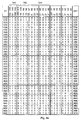
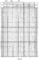
- Figures 4 and 5 show step sequence tables for Step switch mechanisms of a control device according to the invention for an example where five light barriers are independent controlled and queried.
- Figure 4 consists of the Sub-figures 4a and 4b and shows the step sequence table for the first stepping mechanism 8A according to FIG. 3, while Figure 5 (consisting of the partial figures 5a and 5b) one Step sequence table for the second step switch 8B represents.
- ST a description of each step is given.
- the digital states of inputs A0 to A14 are shown, which is the address of the memory location being controlled of the ROM. You can be in a first Partial address TA1, a second partial address TA2 and one Divide the third partial address TA3.
- the digital states at the outputs V0 to V7 for the given step correspond to the content the memory locations controlled by inputs A0 to A14, that in the manufacture of the electronics unit be programmed.
- the column ZST gives the Target step, which is the next step of the ROM step switch is controlled.
- the lines of the step sequence table marked with N show the states of the inputs and outputs in normal operation, i.e. in the event that the second partial address a working and uninterrupted Corresponds to the light barrier.
- the basic function is there Similar to Figures 1 and 2.
- the control of the The light transmitter is switched on at the feedback outputs Q0 to Q2 adjacent bit patterns are set, which are cyclical to repeat. All of the return outputs Bit patterns present at V0 to V6 form that Partial address TA1 of the next step, the together with a second partial address TA2 (inputs A7 to A10), the undisturbed state of each controlled
- the light barrier corresponds to that storage location of the ROM addressed in which the next first Partial address of the normal operating cycle is saved.
- the useful signal output Q7 generates a normal operation output sequence. Any deviation from the specified bit patterns results to exit the normal operating cycle.
- the invention is distinguished from the simple version of Figures 1 and 2 by a number of special features from through the interaction of the two Step switches in a simple way an extremely high one Security standard is achieved.
- a first peculiarity is that the number of Signal feedback is significantly higher than for control of the light barriers necessary.
- feedback outputs Q0 to Q2 are four further outputs of the Step switch traced back to its input.
- One these feedback outputs, output Q6, serve (as with EF 0 371 317) as transmitter activation input.
- the Bit patterns at inputs A0 to A2 are repeated in two successive steps, so that each light barrier controlled twice in a row becomes. However, it is only one step at a time in operation, namely when that at the transmitter activation input A6 applied signal S is an H signal.
- the ST column are the steps in which the light transmitter is in operation, labeled "E" at the last position, during the steps where the light transmitter is switched off, are labeled "A".
- the middle The position of the step name indicates the currently activated Light barrier.
- N1E a step in which the first light barrier is switched on.
- Signals S like EP 0 371 317, can malfunction of the light barriers can be recognized.
- Three further signal feedbacks from the stepping switches 8A and 8B refer to additional outputs Q3 to Q5 or inputs A3 to A5.
- the further signal feedback enable the control of the other blocks with the additional functions realized as a result.
- a third group of peculiarities relates to the consequences of the digital states of the normal operation output sequences of the two step switches 8A and 8B. They are preferably irregular, i.e. within the Normal operating cycle, the H and L states do not change periodically regular, but form a pulse train, in which the H states and / or the L states within are of different lengths. In contrast to the EP 0 371 317 is not used for every successful light barrier query generates an AT signal. Preferably distinguish the consequences of the digital states of the output sequences both stepping mechanisms from each other. The The following explanations make sense of these measures clear from Figure 6.
- Figure 6 consists of the sub-figures 6a to 6c.
- Step numbers ST are given in the header.
- the next step ends with the end of each figure Arrow indicated.
- the next two lines show the consequences the digital states of the useful signals AT1 and AT2 during the specified blocks, ie Figure 6a for the Block V, Figure 6b for block A, Figure 6c for the block N.
- the other lines show the consequences of digital States at output Q3 of stepper 8B (Z1B), at the output 26a of the monoflop 26, at the output 27a of the monoflop 27 and at the inputs A12 of both ROM (RM).
- the output signals AT1 and AT2 trigger the monoflops 26 or 27. They each generate an output pulse MM5 or MM6 of predetermined duration.
- the pulse duration of the monoflop depending on the Duty cycle of signal Z1B, can be increased in two stages, namely from a basic value (for example 0.48 seconds) to a first increased value (e.g. 0.69 Seconds), if Z1B maximum for the duration of an AT1 pulse is applied and to a second increased value (e.g. 1.02 seconds) if Z1B is applied longer.
- a pulse duration extension in three or more stages is possible in a corresponding manner.
- the output signals AT1 and AT2 are only during a fraction (in in practice less than 35% of the normal operating cycle on H.
- the signal RM corresponds to the current flow through the transistors T1 and T2. Only if both transistors on their Are controlled, the coil current flows through the relay unit 20.
- Figure 6c shows that this condition (RM equals H) only for a fraction of clearly less than 50% of the total duration of the normal operating cycle is satisfied.
- the average supply voltage of the relay unit 20 is therefore only one corresponding Fraction of the total supply voltage. This tension is dimensioned so that the withstand voltage of the Relay in the relay unit 20 corresponds. The relays are therefore only operated with their holding voltage and fall off very quickly in the event of a malfunction.
- the normal operation output sequences of the signals AT1 and AT2 are preferably determined so that each of the transistors T1 and T2 at least once in the normal operating cycle isolated (i.e. without simultaneously controlling the other Transistor) is driven. If the other Transistor is working properly and consequently blocks, the feedback signal RM is L and the normal operating cycle to be continued. However, if one the transistors have a short circuit damage, leads the isolated control of the other transistor to one H signal at the feedback inputs A11 and thus too a deviation from the predetermined sequence of steps of the Normal operating cycle and to generate a safety signal. Also an uncontrolled change (“drift away") the pulse duration of the monoflops 26 and 27 or the On-off times of the clock generator 13 lead to a deviation from the predetermined bit pattern of the normal duty cycle and thus to generate a security signal.
- drift away the pulse duration of the monoflops 26 and 27 or the On-off times of the clock generator 13 lead to a deviation from the predetermined bit pattern of the normal duty cycle and thus to generate a security signal.
- Steps 4 and 5 shown apply to the Case that no errors occur during these blocks.
- the lead block it is checked whether the light barriers are functional (i.e. all elements of the light barrier work and the light path is clear). It corresponds (similar to EP 0 371 317) largely a normal operating block, but at the useful signal outputs a pre-run output sequence is generated that is not yet leads to the operating signal of the electronic unit.
- the useful signal output is not always on L, but in at least jumps one step to H, but apart from that excluded from the last double step of the lead block is that the useful signal outputs Q7 both Step switches are simultaneously on H. This allows a short circuit test of transistors T1 and T2 (as described above) already during the run.
- the suit block essentially the same light barrier query as for the normal operating block instead, however, the suit block with regard to those required to attract the relays in the relay unit 20 Time regardless of the number of light barriers always the same length.
- the pull-in block serves the coils 21a, 21b of the relays in the relay unit 20 briefly compared with one to the normal operation significantly increased tightening voltage to act to quickly tighten the relay to reach. Therefore, the signals have AT1 and AT2 at the useful signal outputs Q7 with every "good" light barrier query (Photo eye works and is free) an H signal. It also uses the signal Z1B extends the duration of the monoflop 26. this leads to that the output signals shown in Figure 6b MM5 and MM6 are high throughout the suit block.
- RM is always high, so the full Supply voltage at the relay coils of the relay unit 20 is present.
- a practical example uses a supply voltage worked by 24 volts during the suit block to a very fast suit of a relay type leads, the coils for a nominal voltage of 12 volts are designed.
- the supply voltage of the coils to a holding voltage reduced by, for example, 4 volts so that the relays the relay unit 20 fall off very quickly in the event of a fault.
- the empty block L is in the practical With regard to the operation of the clock generator 13 required.
- the clock generator is dependent on controlled the signal S, which it from the clock output Q6 the step switch 8A is supplied.
- the signal S changes the level after each light barrier query.
- an OFF query must first be carried out. There this OFF query for the light barrier monitoring is not the step is called an empty step.
- G means that those labeled with it Inputs either all the value 1 or all the value Have 0.
- the empty step leads in the manner shown and way to repeat the bad ON query in repetition block W.
- the steps of the repeat block W agree with the corresponding normal operating steps are identical, i.e. the same light barrier that previously had a fault had occurred (both interruption errors at ON queries as well as errors with OFF queries) will be repeated queried. This is to avoid faulty shutdowns be particularly by electromagnetic Influences or caused by extraneous light disturbances can.
- the fault block marked with the letter S. is used in the event of a fault during the ON query show interrupted light barrier.
- the letter A in the S block means all addresses when interrupted a light barrier in one of the blocks V, A or W. become.
- the display of the interrupted light barrier is achieved in that the bit pattern on the Outputs Q0 to Q2 controls the interrupted light barrier, i.e. with the bit pattern at inputs A0 to A2 is identical.
- the step switch remains in the fault state.
- HF Hardware error
- HFF HFF
- the memory locations of the two ROM 11A and 11B, which are in the entire cycle of operation of the ROM stepper 8A and 8B are not used, at least regarding the feedback outputs V0 to V6 be so determined that for any condition on the rest Inputs of the ROM (which have no feedback inputs are) no normal operating output sequence at the useful signal outputs Q7 can be generated.
- the invention allows simple and safety devices can be queried without changing the hardware with a different number of Light barriers.
- the blocks N, U, L and W adjusted according to the principles explained above.
- the pulse sequences are shown in FIG. 6a for clarification for six and seven light barriers as dashed lines Lines drawn.
- Light barriers are directly (without the encoders 16A and 16B) to the Inputs A7 to A10 of ROM 11A and 11B applied. To the same sequence of steps as for five to eight light barriers To be able to use it is useful to use the light barriers to be queried several times.
- control unit shown only has eight light barriers can be controlled separately, it is possible with the same components in the ROM paces 8A and 8B also control a larger number of light barriers. For this, additional compression must take place on the input side, by a total of the specified number of inputs of the EPROM. If instead of the one shown simple priority encoder somewhat more complex Components used to reduce the input signals, the adaptation to a larger number of light barriers is easy possible. For example, a "smarter Compressor "used on the basis of microprocessor technology become. This is especially true if the number of Light barriers are raised beyond sixteen and / or if special functions, such as the temporary shutdown individual light barriers for the purpose of passage of machining parts to be realized. In simpler ones In some cases, an EPROM with sixteen inputs can be used Compression of sixteen light barriers to five outputs be used.
- the invention provides significant advantages achieved compared to the prior art.
- the EP 0 371 317 already enables a very high level of security with little effort. Even against this previously known document is without the invention the safety standard again worth noting increases and at the same time the universal convertibility the control unit to different numbers of light barriers without hardware modification (only by the Change in the control of the setting inputs) reached.
Landscapes
- Physics & Mathematics (AREA)
- Life Sciences & Earth Sciences (AREA)
- General Life Sciences & Earth Sciences (AREA)
- General Physics & Mathematics (AREA)
- Geophysics (AREA)
- Safety Devices In Control Systems (AREA)
- Operating, Guiding And Securing Of Roll- Type Closing Members (AREA)
- Optical Communication System (AREA)
Abstract
Description
- Fig. 1
- Ein Blockschaltbild von einer Lichtschranken-Sicherheitseinrichtung mit einem Steuergerät mit Schrittschaltwerk nach dem Stand der Technik.
- Fig. 2
- Eine Schrittfolge-Tabelle zur Erläuterung der Funktion des Steuergerätes nach Figur 1
- Fig. 3
- Ein Blockschaltbild der Elektronikeinheit eines erfindungsgemäßen Steuergerätes
- Fig. 4 und Fig. 5
- Schrittfolge-Tabellen zur Erläuterung der Funktion der Elektronikeinheit gemäß Fig. 3.
- Fig. 6
- Ein Impulsdiagramm verschiedener Impuls-Sequenzen der Elektronikeinheit gemäß Fig. 3.
Claims (17)
- Lichtschrankensteuergerät für mehrere Lichtschranken (2-5), die jeweils einen Lichtsender und einen Lichtempfänger aufweisen, mit einer Elektronikeinheit (15) an der die Signale der Lichtschranken (2-5) anliegen und die ein Sicherheitssignal erzeugt, wenn mindestens eine Lichtschranke unterbrochen wird, wobeidie Elektronikeinheit ein ROM-Schrittschaltwerk (8) enthält, welches ein ROM (11), einen dem ROM nachgeordneten Schrittspeicher (12) mit mindestens N bistabilen Speicherstellen und einen Taktgenerator (13), der zur Taktung des Schrittspeichers dient, aufweist,mindestens ein Teil N der Ausgänge des ROM (11) als Rückführungsausgänge (V0-V6) an N Rückführungseingängen (D0-D6) des Schrittspeichers (12) anliegt,die entsprechenden N Rückführungsausgänge (Q0-Q6) des Schrittspeichers (12) auf Rückführungseingänge (A0-A6) des ROM (11) zurückgeführt sind, so daß das jeweils an den Rückführungsausgängen (Q0-Q6) des Schrittspeichers (12) anliegende N-Bit-Wort einen Teil der am Eingang des ROM (11) anliegenden Adresse (erste Teiladresse) bildet und das jeweils an den Rückführungsausgängen (V0-V6) des ROM (11) anliegende N-Bit-Wort nach Taktung des Schrittspeichers (12) die nächstfolgende erste Teiladresse bildet,mindestens ein Teil der Ausgänge des ROM-Schrittschaltwerkes (8) als Ansteuerungsausgänge (Q0-Q2) verwendet wird, um Signale zum Ansteuern der Lichtsender zu erzeugen,ein Teil der Eingänge des ROM als Empfängereingänge (A7-A10) dient, an denen Empfängersignale anliegen, so daß sie eine zweite Teiladresse des ROM (11) bilden,mindestens einer der Ausgänge des ROM-Schrittschaltwerkes (8) als Nutzsignalausgang (Q7) dient, der mit einer Sicherheitsignal-Erzeugungseinrichtung (10) verbunden ist,die durch die Gesamtadresse aus erster Teiladresse und zweiter Teiladresse bestimmten Speicherstellen des ROM für den Fall, daß die zweite Teiladresse einer funktionierenden ununterbrochenen Lichtschranke entspricht (Normalbetriebsfall) eine vorbestimmte Folge von Bit-Mustern enthalten, bei der sich die an den Rückführungsausgängen (V0-V6) anliegenden N-Bit-Worte zyklisch wiederholen, so daß sich die Schrittfolge des ROM-Schrittschaltwerkes (8) innerhalb eines Normalbetriebszyklus ebenfalls zyklisch wiederholt und die Lichtschranken über die Ansteuerungsausgänge (Q0-Q2) zyklisch angesteuert werden, wobei an dem Nutzsignalausgang (Q7) des ROM-Schrittschaltwerkes eine vorbestimmte Folge von digitalen Impulsen als Normalbetriebs-Ausgangssequenz erzeugt wird unddie durch die Gesamtadresse aus erster Teiladresse und zweiter Teiladresse bestimmten Speicherstellen des ROM (11) für den Fall, daß die zweite Teiladresse nicht einer ununterbrochenen Lichtschranke entspricht (Störfall) einen von der vorbestimmten Folge von Bit-Mustern des Normalbetriebszyklus abweichenden Speicherinhalt enthalten, so daß der Normalbetriebszyklus unterbrochen und an dem Nutzsignalausgang (Q7) ein Störfall-Ausgangssignal erzeugt wird, aufgrund dessen die Sicherheitssignal-Erzeugungseinrichtung (10) das Sicherheitssignal erzeugt,
dadurch gekennzeichnet,daß die Elektronikeinheit zwei ROM-Schrittschaltwerke (8A, 8B) mit jeweils einem ROM (11A, 11B) und einem nachgeordneten Schrittspeicher (12A, 12B) enthält, jedes ROM Empfängereingänge (A7-A10) aufweist, an denen Empfängersignale anliegen, die beiden ROM-Schrittschaltwerke (8A, 8B) synchron getaktet sind und die Nutzsignalausgänge (Q7) beider Schrittschaltwerke (8A, 8B) mit einer gemeinsamen Sicherheitssignal-Erzeugungseinrichtung (10) verbunden sind, die ein Sicherheitssignal erzeugt, wenn an dem Nutzsignalausgang (Q7) von mindestens einem der Schrittschaltwerke (8A, 8B) ein Störfall-Ausgangssignal erzeugt wird. - Lichtschrankensteuergerät nach Anspruch 1, dadurch gekennzeichnet, daß die Speicherinhalte der beiden ROM (11A, 11B) so bestimmt sind, daß die Folgen der digitalen Zustände der Normalbetriebs-Ausgangssequenzen beider Schrittschaltwerke (8A, 8B) unterschiedlich sind.
- Lichtschrankensteuergerät nach einem der vorhergehenden Ansprüche, dadurch gekennzeichnet, daß die Folge der digitalen Zustände der Normalbetriebs-Ausgangssequenz von mindestens einem der Schrittschaltwerke (8A, 8B) unregelmäßig ist.
- Lichtschrankensteuergerät nach einem der vorhergehenden Ansprüche, dadurch gekennzeichnet, daß die Sicherheitssignal-Erzeugungseinrichtung (10) eine Verknüpfungsschaltung (19) aufweist, durch die die beiden Ausgangssignale der Schrittschaltwerke (8A, 8B) im Sinne einer logischen "und"-Verknüpfung verknüpft werden.
- Lichtschrankensteuergerät nach Anspruch 4, dadurch gekennzeichnet, daß die Sicherheitssignal-Erzeugungseinrichtung (10) als Verknüpfungsschaltung (19) zwei in Reihe geschaltete Schaltelemente (T1, T2), insbesondere Schalttransistoren, aufweist.
- Lichtschrankensteuergeräte nach Anspruch 5, dadurch gekennzeichnet, daß die Dauer der Ansteuerung der Schaltelemente (T1, T2) von der Folge der digitalen Zustände der Normalbetriebs-Ausgangssequenz beeinflußt wird.
- Lichtschrankensteuergerät nach einem der Ansprüche 5 oder 6, dadurch gekennzeichnet, daß die Reihenschaltung der Schaltelemente (T1, T2) mit einer Sicherung abgesichert ist, die Schaltelemente im Normalbetriebszyklus derartig angesteuert werden, daß beide Schaltelemente während einer Schließzeit von weniger als der Hälfte des Normalbetriebszyklus gleichzeitig geschlossen sind und der Grenzwert der Sicherung so gewählt ist, daß sie bei Überschreiten dieser maximalen Schließzeit anspricht.
- Lichtschrankensteuergerät nach einem der vorhergehenden Ansprüche, dadurch gekennzeichnet, daß die Sicherheitssignal-Erzeugungseinrichtung (10) einen monostabilen Multivibrator (26) aufweist, mit dessen Eingang ein Nutzsignalausgang (Q7) eines Schrittschaltwerkes (8) so verbunden ist, daß er von Flanken der digitalen Zustände von dessen Normalbetriebs-Ausgangssequenz getriggert wird, um ausgangsseitig einen Impuls von vorbestimmter Dauer zur Weiterverarbeitung in der Sicherheitssignal-Erzeugungseinrichtung (10) zu generieren.
- Lichtschrankensteuergerät nach Anspruch 8, dadurch gekennzeichnet, daß die vorbestimmte Dauer des Impulses des monostabilen Multivibrators (26, 27) in Abhängigkeit von einem Ausgangssignal (Z1B) eines Schrittschaltwerkes (8), vorzugsweise mehrstufig, einstellbar ist.
- Lichtschrankensteuergerät nach einem der Ansprüche 8 oder 9, dadurch gekennzeichnet, daß die Sicherheitssignal-Erzeugungseinrichtung zwei monostabile Multivibratoren (26,27) mit vorzugsweise unterschiedlicher Impulsdauer aufweist, die mit je einem Nutzsignalausgang (Q7) der beiden Schrittschaltwerke (8A, 8B) verbunden sind.
- Lichtschrankensteuergerät nach Anspruch 10 in Verbindung mit Anspruch 5, dadurch gekennzeichnet, daß die Ausgänge der monostabilen Multivibratoren (26, 27) mit den Eingängen der Schaltelemente (T1, T2) zu deren Ansteuerung verbunden sind.
- Lichtschrankensteuergerät nach einem der vorhergehenden Ansprüche, dadurch gekennzeichnet, daß die Sicherheitssignalerzeugungseinrichtung (10) mit einem als Rückmeldungseingang (A11) dienenden Eingang von mindestens einem ROM verbunden ist, um wahrend des Normalbetriebszyklus eine Überprüfung ihrer Funktion zu ermöglichen.
- Lichtschrankensteuergerät nach einem der vorhergehenden Ansprüche, dadurch gekennzeichnet, daß je ein Eingang der beiden ROM (11A, 11B) als Partnerüberwachungseingang (A12) dient, der zur Überprüfung der Funktion des jeweils anderen Schrittschaltwerkes (8A, 8B) mit dessen Nutzsignalausgang (Q7) verbunden ist.
- Lichtschrankensteuergerät nach einem der vorhergehenden Ansprüche, dadurch gekennzeichnet, daß ein Teil der Eingänge der ROM (11A, 11B) als Einstelheingänge (A13, A14) dient, an die individuell einstellbare Schalter (17A, 17B) angeschlossen sind, um das Lichtschrankensteuergerät auf verschiedene Betriebszustände einzustellen, die sich hinsichtlich der Anzahl der Lichtschranken unterscheiden.
- Lichtschrankensteuergerät nach einem der vorhergehenden Ansprüche, dadurch gekennzeichnet, daß der Speicherinhalt der beiden ROM (11A, 11B) so vorbestimmt ist, daß bei Unterbrechung einer Lichtschranke ein Wiederholschritt durchgeführt wird, bei dem die gleiche Lichtschranke nochmals angesteuert wird.
- Lichtschrankensteuergerät nach einem der vorhergehenden Ansprüche, dadurch gekennzeichnet, daß die Speicherinhalte der beiden ROM (11A, 11B) so vorbestimmt sind, daß die vorbestimmte Schrittfolge der beiden Schrittschaltwerke (8A, 8B) einen Anzugsblock einschließt, in dem an dem Nutzsignalausgang eine Folge von digitalen Impulsen als Anzugsblock-Ausgangssequenz erzeugt wird, wobei die Impulsdichte in der Anzugsblock-Ausgangssequenz höher als in der Normalbetriebs-Ausgangssequenz ist.
- Lichtschrankensteuergerät nach einem der vorhergehenden Ansprüche, dadurch gekennzeichnet, daß die Speicherstellen der beiden ROM (11A, 11B), die in dem gesamten Betriebszyklus des jeweiligen ROM-Schrittschaltwerkes nicht verwendet werden, hinsichtlich der Rückführungsausgänge V0 bis V6 so bestimmt sind, daß für beliebige Zustände an den übrigen Eingängen des ROM keine Normalbetriebsausgangssequenz erzeugt werden kann.
Applications Claiming Priority (2)
| Application Number | Priority Date | Filing Date | Title |
|---|---|---|---|
| DE19849502 | 1998-10-27 | ||
| DE1998149502 DE19849502C1 (de) | 1998-10-27 | 1998-10-27 | Lichtschrankensteuergerät |
Publications (2)
| Publication Number | Publication Date |
|---|---|
| EP0997859A2 true EP0997859A2 (de) | 2000-05-03 |
| EP0997859A3 EP0997859A3 (de) | 2003-04-02 |
Family
ID=7885799
Family Applications (1)
| Application Number | Title | Priority Date | Filing Date |
|---|---|---|---|
| EP99121290A Withdrawn EP0997859A3 (de) | 1998-10-27 | 1999-10-26 | Lichtschrankensteuergerät |
Country Status (2)
| Country | Link |
|---|---|
| EP (1) | EP0997859A3 (de) |
| DE (1) | DE19849502C1 (de) |
Cited By (1)
| Publication number | Priority date | Publication date | Assignee | Title |
|---|---|---|---|---|
| WO2009137743A2 (en) | 2008-05-09 | 2009-11-12 | Omron Scientific Technologies, Inc. | Method and apparatus for zone selection in area monitoring devices |
Families Citing this family (1)
| Publication number | Priority date | Publication date | Assignee | Title |
|---|---|---|---|---|
| CN110133746B (zh) * | 2018-02-08 | 2024-06-04 | 莫祥有 | 饲料采样装置及水产饲喂设备 |
Family Cites Families (1)
| Publication number | Priority date | Publication date | Assignee | Title |
|---|---|---|---|---|
| DE3840493C1 (de) * | 1988-12-01 | 1990-01-25 | Werac Elektronik Gmbh, 6729 Woerth, De |
-
1998
- 1998-10-27 DE DE1998149502 patent/DE19849502C1/de not_active Expired - Fee Related
-
1999
- 1999-10-26 EP EP99121290A patent/EP0997859A3/de not_active Withdrawn
Cited By (4)
| Publication number | Priority date | Publication date | Assignee | Title |
|---|---|---|---|---|
| WO2009137743A2 (en) | 2008-05-09 | 2009-11-12 | Omron Scientific Technologies, Inc. | Method and apparatus for zone selection in area monitoring devices |
| WO2009137743A3 (en) * | 2008-05-09 | 2010-11-18 | Omron Scientific Technologies, Inc. | Method and apparatus for zone selection in area monitoring devices |
| US8018353B2 (en) | 2008-05-09 | 2011-09-13 | Omron Scientic Technologies, Inc. | Method and apparatus for zone selection in area monitoring devices |
| EP2274680B1 (de) | 2008-05-09 | 2025-03-26 | Omron Scientific Technologies, INC. | Verfahren und vorrichtung zur zonenauswahl in bereichsüberwachungsgeräten |
Also Published As
| Publication number | Publication date |
|---|---|
| EP0997859A3 (de) | 2003-04-02 |
| DE19849502C1 (de) | 1999-10-07 |
Similar Documents
| Publication | Publication Date | Title |
|---|---|---|
| EP1269274B2 (de) | Sicherheitsschaltgerät und verfahren zur einstellung eines betriebsmodus eines sicherheitsschaltgeräts | |
| DE2923511C3 (de) | Elektronische Einrichtung zur Überwachung einer Mehrzahl laufender Fäden an einer Textilmaschine | |
| EP3043220B1 (de) | Vorrichtung und verfahren zur funktionsüberwachung eines sicherheitsschaltmittels | |
| DE2059797B1 (de) | Taktversorgungsanlage | |
| DE2453011A1 (de) | Verfahren und schaltungsanordnung zur auswahl eines signals aus wenigstens drei redundanten signalkanaelen | |
| EP0371317B1 (de) | Lichtschranken-Sicherheitseinrichtung | |
| DE3109638A1 (de) | Schutz- und ueberwachungseinrichtung fuer steuerschaltungsanordnungn in kraftfahrzeugen | |
| DE3522220C2 (de) | Schaltungsanordnung zur sicheren Ansteuerung von Stellelementen eines Prozesses | |
| EP1594021B1 (de) | Schaltungsanordnung sowie Verfahren zum Testen von Relaisschaltkontakten einer digitalen Ausgangsschaltung | |
| EP2127992A2 (de) | Schaltung zur Überwachung von Endlagenschaltern eines 4-Draht-Drehstrom-Antriebs einer Weiche | |
| DE2228320A1 (de) | Rundsteuerempfaenger | |
| DE4004427C2 (de) | Diagnostisches Störungsmeldesystem | |
| EP0505774B1 (de) | Sicherheitsschaltgerät | |
| EP0997859A2 (de) | Lichtschrankensteuergerät | |
| EP1430458B1 (de) | Verfahren zum überwachen einer automatisierungsanlage | |
| DE2255031C3 (de) | Schaltungsanordnung für einen Baustein zum Aufbau fehlersicherer Schutzschaltungen | |
| EP0864875A2 (de) | Verfahren zur Überprüfung einer Sicherheitsschaltung | |
| DE2047878C (de) | Schaltungsanordnung fur Fernmelde Vermittlungsanlagen, insbesondere Fern sprech Vermittlungsanlagen, mit Prüf und Belegungsstromkreisen | |
| DE3426047C2 (de) | ||
| DE2612532A1 (de) | Schaltungsanordnung zur ueberwachung von zeitlich gestaffelt mehreren leitungen jeweils als taktimpulsfolge zugeordnete taktimpuls | |
| DE2613927C3 (de) | Schaltungsanordnung zur Steuerung und Überwachung der Abfrage von Signalquellen mit individuellen Signalleitungen | |
| DE1762221C3 (de) | Ausfallsicheres binäres Schaltnetz | |
| DE2427798B2 (de) | Steuerschaltung für das Eingangssignal bei binären elektronischen Zählstufen | |
| DE2705190B2 (de) | Schaltungsanordnung zur Überwachung von Signalleitungen in Fernmelde-, insbesondere Fernsprechanlagen | |
| DE1538662C (de) | Verfahren zur elektronischen Steuerung elektrischer Schalter mit Impulsbildtelegrammen |
Legal Events
| Date | Code | Title | Description |
|---|---|---|---|
| PUAI | Public reference made under article 153(3) epc to a published international application that has entered the european phase |
Free format text: ORIGINAL CODE: 0009012 |
|
| AK | Designated contracting states |
Kind code of ref document: A2 Designated state(s): AT BE CH CY DE DK ES FI FR GB GR IE IT LI LU MC NL PT SE |
|
| AX | Request for extension of the european patent |
Free format text: AL;LT;LV;MK;RO;SI |
|
| PUAL | Search report despatched |
Free format text: ORIGINAL CODE: 0009013 |
|
| AK | Designated contracting states |
Kind code of ref document: A3 Designated state(s): AT BE CH CY DE DK ES FI FR GB GR IE IT LI LU MC NL PT SE Designated state(s): AT BE CH CY DE DK ES FI FR GB GR IE IT LI LU MC NL PT SE |
|
| AX | Request for extension of the european patent |
Extension state: AL LT LV MK RO SI |
|
| 17P | Request for examination filed |
Effective date: 20030712 |
|
| GRAP | Despatch of communication of intention to grant a patent |
Free format text: ORIGINAL CODE: EPIDOSNIGR1 |
|
| AKX | Designation fees paid |
Designated state(s): DE FR GB |
|
| STAA | Information on the status of an ep patent application or granted ep patent |
Free format text: STATUS: THE APPLICATION IS DEEMED TO BE WITHDRAWN |
|
| 18D | Application deemed to be withdrawn |
Effective date: 20040211 |