EP0988614B1 - Verfahren und gerät zum messen der strukturen eines fingerabdrucks - Google Patents
Verfahren und gerät zum messen der strukturen eines fingerabdrucks Download PDFInfo
- Publication number
- EP0988614B1 EP0988614B1 EP98928665A EP98928665A EP0988614B1 EP 0988614 B1 EP0988614 B1 EP 0988614B1 EP 98928665 A EP98928665 A EP 98928665A EP 98928665 A EP98928665 A EP 98928665A EP 0988614 B1 EP0988614 B1 EP 0988614B1
- Authority
- EP
- European Patent Office
- Prior art keywords
- sensors
- sensor array
- measuring
- sensor
- essentially
- Prior art date
- Legal status (The legal status is an assumption and is not a legal conclusion. Google has not performed a legal analysis and makes no representation as to the accuracy of the status listed.)
- Expired - Lifetime
Links
Images

Classifications
-
- G—PHYSICS
- G06—COMPUTING; CALCULATING OR COUNTING
- G06V—IMAGE OR VIDEO RECOGNITION OR UNDERSTANDING
- G06V40/00—Recognition of biometric, human-related or animal-related patterns in image or video data
- G06V40/10—Human or animal bodies, e.g. vehicle occupants or pedestrians; Body parts, e.g. hands
- G06V40/12—Fingerprints or palmprints
- G06V40/1335—Combining adjacent partial images (e.g. slices) to create a composite input or reference pattern; Tracking a sweeping finger movement
-
- G—PHYSICS
- G06—COMPUTING; CALCULATING OR COUNTING
- G06V—IMAGE OR VIDEO RECOGNITION OR UNDERSTANDING
- G06V40/00—Recognition of biometric, human-related or animal-related patterns in image or video data
- G06V40/10—Human or animal bodies, e.g. vehicle occupants or pedestrians; Body parts, e.g. hands
- G06V40/12—Fingerprints or palmprints
- G06V40/13—Sensors therefor
- G06V40/1306—Sensors therefor non-optical, e.g. ultrasonic or capacitive sensing
-
- A—HUMAN NECESSITIES
- A61—MEDICAL OR VETERINARY SCIENCE; HYGIENE
- A61B—DIAGNOSIS; SURGERY; IDENTIFICATION
- A61B5/00—Measuring for diagnostic purposes; Identification of persons
- A61B5/117—Identification of persons
- A61B5/1171—Identification of persons based on the shapes or appearances of their bodies or parts thereof
- A61B5/1172—Identification of persons based on the shapes or appearances of their bodies or parts thereof using fingerprinting
Definitions
- the invention relates to a method and an apparatus for the measuring of structures in a fingerprint or the like, comprising the measuring of chosen characteristics of the surface of the fingerprint, e.g. capacitance or resistivity, using a sensor array comprising a plurality of sensors, positioned in contact with, or close to, the surface.
- chosen characteristics of the surface of the fingerprint e.g. capacitance or resistivity
- Some of the previously known solutions are based upon optical technology using light with one or more wavelengths. These are sensitive to dirt and contamination, both in the fingerprint and on the sensor surface, and thus cleaning is necessary for both.
- fingerprint sensors may be exposed to long term use in varying and sometimes demanding conditions the sensor needs to have a robust surface and to be as insensitive to pollution in the fingerprint and on the sensor as possible. It must be capable of reading most fingerprints without being disturbed by latent prints from earlier use. In some cases, e.g. in credit cards or computer keyboards, it would also be advantageous if the sensor could be made compact.
- EP 735.502 describes the use of a one or two-dimensional array of sensors being moved in relation to the finger print.
- the described solution is based on the measuring of resistance, and has a limited resolution defined by the minimum sensor dimensions and the distance between the sensors.
- the present invention provides a method and an apparatus for the measuring of structures in a fingerprint or the like, for example using one of the techniques described above, characterized as stated in the disclosed claims 1 and 6.
- the surface of the sensor array is small, and contains few sensors compared to the known solutions, it is inexpensive and relatively simple to make. As the fingerprint to be measured is moved past the sensor array there is no latent fingerprint remaining from the previous user, giving another advantage in relation to the known finger print sensors.
- the apparatus and method according to the invention comprises two or more parallel lines of measuring points, each line of measuring points being shifted in the longitudinal direction with a distance less than the distance between the measuring points, the sensor array comprising two or more parallel lines of equally spaced sensors, preferably shifted in the longitudinal direction of the sensor array.
- essentially one-dimensional array here refers to an array having a length being much larger than its width, and may comprise more than one line of sensors.
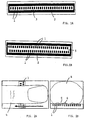
- FIG 1a a single, linear array of sensors 1 is shown.
- the sensors may be of different kinds, such as pressure sensors or temperature sensors, but preferably they are electrical conductors providing a possibility to measure conduction, impedance or capacitance of the different parts of the fingerprint.
- the surface to be measured is moved in a perpendicular direction relative to the line of sensors.
- the sensors 1 are electrical conductors separated by an insulating material 3 such as epoxy.
- an electrically conducting material 2 surrounds the sensors which may be used to provide a reference potential. Thus the conduction, impedance or capacitance, through the fingerprint, between each of the sensors 1 and the surrounding reference level may be measured.
- Figure 1b shows a preferred embodiment of the invention in which the sensor array comprises two lines of sensors 1.
- the array will typically be 10-15 mm long with a resolution of 50 ⁇ m. This is difficult or expensive to obtain using a single line of sensors.
- the lines are slightly shifted in relation to each other.
- the measurements of each of the sensors in the second line will fall between the measured point of the first line, providing the required resolution with a larger distance between the sensors.
- Three or more lines are possible to improve the resolution even more, but more than five would be impractical because of the distance between the lines and the resulting time lapse between the measurements of the first and the last line.
- an apparatus using many lines would be sensitive to the direction in which the finger is moved.
- the shifted, second, third etc. lines may comprise single or groups of sensors, increasing the resolution in certain parts of the finger print, and/or measuring differences in velocity of different parts of the finger print, in case the movements is uneven. Also, the second, third etc. lines may have an angle in relation to the first line of sensors.
- the measurements of the different lines must be combined to provide a signal corresponding to one single line of sensors.
- the signals from the sensors must be adjusted for the time delay between the signals from the sensors in different lines, and thus the movement of the finger in relation to the sensor array must be known, either by moving the finger or sensor array with a chosen speed, or by measuring the movement of the finger.
- Figure 2a illustrates how the finger 4 is moved over a sensor array in the direction perpendicular to the array.
- the movement of the finger must be measured.
- this may be done in many ways, such as providing a rotating cylinder in contact with the finger, so that the rotation of the cylinder may be measured.
- Another example may be the use of a thin disk on which the finger may be positioned, which is moved together with the finger and is connected to the apparatus so that the velocity of the disk may be measured.
- the movement is measured by correlating or comparing the signals from the different sensor lines, and the time lapse or spacial shift between the measurements of corresponding structures in the surface is found. This way more detailed images can be made from the separate images of each line of sensors.
- Another method for adjusting for the movement of the finger is to maintain the sampling rate at the sensor array, while adjusting the number of measured lines used in generating the segmented image of the surface, and thus the interval of the measurements according to movement in order to obtain at least one measurement of each portion of the surface. For example, if the fingerprint is moved slowly over the sensor, while the sampling or measuring frequency is high, the redundant data may simply be neglected and the image of the finger print is comprised by each second or third set of data.
- Figure 2b shows a cross section of the finger 4 placed on the sensors 1, and also shows an exaggerated view of the ridges 5 and valleys 6 in the fingerprint.
- Figure 3 shows a simplified view of the apparatus according to the invention comprising conductors 7 from the sensors 1 to an amplifier and multiplexer 8. The signal is then digitized in an A/D-converter 9 before the digital signal is sent to a computer 10 comprising any available computer program being able to analyse the signal.
- FIG 4 A cross section of a more realistic embodiment is shown in figure 4, in which one end of closely spaced conductors 11 represent the sensors, and the other end of these conductors are connected to a microchip.
- the conductors 11 may be a part of a multi layer printed circuit board moulded in epoxy, producing two or more lines of sensors. Each sensor 1 would be about 35 ⁇ 50 ⁇ m. If the sensors in each line is mounted with distance between the centres of 150 ⁇ m, the resolution with three shifted lines will be 50 ⁇ m.
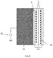
- Figure 5 shows an embodiment of the invention where an external time varying, e.g. oscillating or pulsating, voltage 12 is applied to the finger through the conducting area 14 on the side of the sensor area. Planes at a constant voltage 13 are placed close to and parallel to the conductors 11. This reduces cross-talk and noise from external sources, and improves contrast in the image generated from the measurements.
- This may be implemented by using a multilayer printed circuit board, where one or more of the conducting layers are at a constant voltage.
- An insulating layer (not shown) preferably covers the conductors 1,11 and shielding planes 13.
- the conducting area 14 may also be covered by an insulating layer, but this. would decrease the signal strength.
- the oscillating voltage 12 may be applied to both sides of the sensor surface.
- the oscillating voltage may, as mentioned above, be a pulse train, or a sinus.
- a sinus of 100kHz is applied to the conducting area 14, and each of the conductors 11 is terminated by a resistance, and the signal is amplified and feed to a demodulator, multiplexer and analogue-to-digital converter.
- This solution provides a sensor apparatus being simple to produce using standard techniques, and thus cheap. It is also compact and rugged. If the measured parameter is the resistance the sensors, being the ends of the conductors, will not change their characteristics as they and the surrounding epoxy are worn down. If the capacitance is to be measured a durable, insulating layer is provided on the sensors or conductor ends.
- the preferred layout of the sensor also allows the resolution to be better than the distance between the sensors, reducing cross-talk between the sensors.
- the method and apparatus according to the invention may of course be utilized in many different ways, and different characteristics may be measured in order to provide a representation of the measured surface, in addition to capacitance and/or conductivity.
- Optical detectors may be used, and preferably transmitters, so that the reflected image of the fingerprint may be analysed regarding for example contrast and/or colour.
- the sensors may, as mentioned above simply be the ends of conductors connected to means for measuring capacitance and/or conductivity, or may be sensors made from semiconducting materials.
- a preferred semiconducting material when cost is essential would be silicon.
- an insulating layer (not shown) is provided between the conductor ends and the finger print.
- Another possible embodiment within the scope of this invention comprises sensor lines of not equally spaced sensors positioned to measure chosen parts of the fingerprint.
Claims (14)
- Verfahren zum Messen von Strukturen in einem Fingerabdruck oder dergleichen, umfassend das Messen gewählter Eigenschaften der Fläche des Fingerabdrucks mithilfe einer eine Mehrzahl von Sensoren umfassenden Sensoranordnung, die in Berührung mit oder nahe an einem Teil der Fläche positioniert wird,
umfassend das Messen der genannten Eigenschaften in wenigstens einer Reihe von Messpunkten entlang einem länglichen Teil der Fläche in bestimmten Zeitintervallen,
wobei die Sensoranordnung eine im Wesentlichen eindimensionale Anordnung ist,
Messen der genannten Eigenschaften mithilfe von wenigstens einem Messpunkt, der in einem gewählten Abstand von der genannten Reihe von Messpunkten in einer zur Achse der Reihe lotrechten Richtung positioniert wird,
Bewegen der Fläche im Verhältnis zur Sensoranordnung in einer zur Sensoranordnung lotrechten Richtung, sodass die Messungen an verschiedenen oder teilweise überlappenden Teilen der Fläche durchgeführt werden, und Berechnen der genannten Bewegung anhand der genannten Messungen an der genannten Reihe von Sensoren und dem genannten wenigstens einen Sensor,
Kombinieren der Messungen der gemessenen Teile der Fläche, um eine segmentierte zweidimensionale Darstellung der genannten Eigenschaften der Fläche bereitzustellen,
dadurch gekennzeichnet, dass die Sensoren kapazitive Sensoren sind, die durch eine Isolierhaut von der Fläche getrennt sind, wobei die genannten Sensoren die Aufgabe haben, die Kapazitätsänderungen entlang der Sensoranordnung zu messen, und dass eine variierende Spannung mithilfe einer von der Sensoranordnung separat platzierten Elektrode an die zu messende Fläche angelegt wird. - Verfahren nach Anspruch 1, dadurch gekennzeichnet, dass die Messpunkte der Anordnung entlang der genannten im Wesentlichen eindimensionalen Anordung im Wesentlichen gleich voneinander beabstandet sind.
- Verfahren nach Anspruch 1 oder 2, gekennzeichnet durch das Messen der relativen Bewegung der Fläche und Einstellen des Intervalls der Messungen gemäß der Bewegung, um wenigstens eine Messung jedes Teils der Fläche zu erhalten.
- Verfahren nach Anspruch 1, 2 oder 3, dadurch gekennzeichnet, dass jede Messung der Eigenschaften eines länglichen Teils der Fläche im Wesentlichen gleichzeitiges Messen der genannten Eigenschaften entlang wenigstens zwei Reihen von Messpunkten umfasst, von denen eine den genannten wenigstens einen Messpunkt umfasst,
wobei jede Reihe von Messpunkten in der Längsrichtung mit einem dem Abstand zwischen den Messpunkten nicht gleichen Abstand verschoben ist, wobei die Sensoranordnung zwei oder mehr im Wesentlichen parallele Reihen von im Wesentlichen mit gleichem Zwischenraum zueinander angeordneten Sensoren umfasst, die vorzugsweise in der Längsrichtung der Sensoranordnung verschoben sind. - Verfahren nach einem der vorhergehenden Ansprüche, dadurch gekennzeichnet, dass die Bewegung durch Korrelation der Messungen von verschiedenen Messreihen gemessen wird, um den Zeitverlauf oder die räumliche Verschiebung zwischen den ähnlichen Strukturen an verschiedenen Reihen von Messpunkten festzustellen.
- Vorrichtung zum Messen von Strukturen in einem Fingerabdruck oder dergleichen, umfassend eine Sensoranordnung, die ausgeführt ist, um in Berührung mit oder nahe an einem Teil der Fläche des Fingerabdrucks positioniert zu werden, wobei die Sensoranordnung die Aufgabe hat, gewählte Eigenschaften der Fläche an einer Mehrzahl von Positionen zu messen, z.B. durch Messen von Kapazität oder spezifischem Widerstand,
wobei die Sensoranordnung eine im Wesentlichen eindimensionale, wenigstens eine Reihe von Sensoren umfassende Anordnung ist, die zum Messen der genannten Eigenschaften in gewählten Zeitintervallen ausgeführt ist, wobei die Fläche eine relative Bewegung im Verhältnis zur Sensoranordnung hat mit einer zur Anordnung im Wesentlichen lotrechten Richtung,
und die Vorrichtung wenigstens einen Sensor umfasst, der in einem gewählten Abstand von der genannten Reihe von Sensoren in einer zu der genannten Reihe lotrechten Richtung positioniert ist,
und die Vorrichtung eine Mittel zum Kombinieren der Messungen in den verschiedenen Zeitintervallen zum Erhalten einer segmentierten zweidimensionalen Darstellung der Eigenschaften der Fläche hat,
dadurch gekennzeichnet, dass die Sensoren kapazitive Sensoren zum Messen von Kapazitätsänderungen entlang der Sensoranordnung sind und
dass Spannungsversorgungsmittel zum Anlegen einer im Verhältnis zur Zeit variierenden Spannung an die zu messende Fläche separat von der Sensoranordnung platziert sind und dass ein dünner Isolator die Leiter in der Sensoranordnung von der zu messenden Fläche trennt, wobei die Sensoren im Wesentlichen die kapazitive Kopplung durch die Isolierschicht zwischen der zu messenden Fläche und den Leitern messen. - Vorrichtung nach Anspruch 6, dadurch gekennzeichnet, dass die im Wesentlichen eindimensionale Sensoranordnung zwei oder mehr parallele Reihen von im Wesentlichen mit gleichem Zwischenraum voneinander beabstandeten Sensoren umfasst, wobei der genannte wenigstens eine Sensor in der genannten Anordnung enthalten ist.
- Vorrichtung nach Anspruch 7, dadurch gekennzeichnet, dass die genannten Sensorreihen in der Längsrichtung der Sensoranordnung mit einem dem Abstand zwischen den Sensoren nicht gleichen Abstand verschoben sind.
- Vorrichtung nach Anspruch 6, 7 oder 8, dadurch gekennzeichnet, dass die Vorrichtung eine Einrichtung zum Finden der Bewegung der Fläche im Verhältnis zur Sensoranordnung umfasst.
- Vorrichtung nach Anspruch 9, dadurch gekennzeichnet, dass die Einrichtung Mittel zum Vergleichen der Signale von den verschiedenen Sensorreihen umfasst, um den Zeitverlauf oder die räumliche Verschiebung zwischen den ähnlichen Strukturen an den verschiedenen Sensorreihen zu finden..
- Vorrichtung nach Anspruch 6, dadurch gekennzeichnet, dass die Leiter in der Sensoranordnung im Wesentlichen lotrecht zur zu messenden Fläche platziert sind und dass eine oder mehrere Ebenen konstanter Spannung nahe an und parallel mit den Leitern platziert sind, die sich im Wesentlichen bis zur Isolierschicht erstrecken.
- Vorrichtung nach einem der Ansprüche 6 bis 11, dadurch gekennzeichnet, dass die Sensoren auch Elektroden umfassen, die Schwankungen des elektrischen Widerstands entlang der Sensoranordnung messen können.
- Vorrichtung nach einem der Ansprüche 6 bis 12, dadurch gekennzeichnet, dass die Sensoren auch optische Melder und vorzugsweise optische Sender umfassen.
- Vorrichtung nach einem der Ansprüche 6 bis 13, dadurch gekennzeichnet, dass die Sensoranordnung aus einem halbleitenden Material, vorzugsweise Silizium, hergestellt ist.
Priority Applications (1)
| Application Number | Priority Date | Filing Date | Title |
|---|---|---|---|
| EP02025170A EP1304646B2 (de) | 1997-06-16 | 1998-06-12 | Verfahren zum Messen der Strukturen eines Fingerabrucks mittels eines linearen Sensors |
Applications Claiming Priority (3)
| Application Number | Priority Date | Filing Date | Title |
|---|---|---|---|
| NO972759A NO304766B1 (no) | 1997-06-16 | 1997-06-16 | Fingeravtrykksensor |
| NO972759 | 1997-06-16 | ||
| PCT/NO1998/000182 WO1998058342A1 (en) | 1997-06-16 | 1998-06-12 | Method and apparatus for measuring structures in a fingerprint |
Related Child Applications (1)
| Application Number | Title | Priority Date | Filing Date |
|---|---|---|---|
| EP02025170A Division EP1304646B2 (de) | 1997-06-16 | 1998-06-12 | Verfahren zum Messen der Strukturen eines Fingerabrucks mittels eines linearen Sensors |
Publications (2)
| Publication Number | Publication Date |
|---|---|
| EP0988614A1 EP0988614A1 (de) | 2000-03-29 |
| EP0988614B1 true EP0988614B1 (de) | 2004-09-15 |
Family
ID=19900827
Family Applications (2)
| Application Number | Title | Priority Date | Filing Date |
|---|---|---|---|
| EP02025170A Expired - Lifetime EP1304646B2 (de) | 1997-06-16 | 1998-06-12 | Verfahren zum Messen der Strukturen eines Fingerabrucks mittels eines linearen Sensors |
| EP98928665A Expired - Lifetime EP0988614B1 (de) | 1997-06-16 | 1998-06-12 | Verfahren und gerät zum messen der strukturen eines fingerabdrucks |
Family Applications Before (1)
| Application Number | Title | Priority Date | Filing Date |
|---|---|---|---|
| EP02025170A Expired - Lifetime EP1304646B2 (de) | 1997-06-16 | 1998-06-12 | Verfahren zum Messen der Strukturen eines Fingerabrucks mittels eines linearen Sensors |
Country Status (11)
| Country | Link |
|---|---|
| US (3) | US7110577B1 (de) |
| EP (2) | EP1304646B2 (de) |
| JP (1) | JP4051093B2 (de) |
| AT (2) | ATE276547T1 (de) |
| AU (1) | AU8041498A (de) |
| DE (2) | DE69833337T3 (de) |
| DK (1) | DK1304646T4 (de) |
| ES (1) | ES2258129T5 (de) |
| NO (1) | NO304766B1 (de) |
| PT (1) | PT1304646E (de) |
| WO (1) | WO1998058342A1 (de) |
Cited By (4)
| Publication number | Priority date | Publication date | Assignee | Title |
|---|---|---|---|---|
| US7809211B2 (en) | 2005-11-17 | 2010-10-05 | Upek, Inc. | Image normalization for computed image construction |
| US9501685B2 (en) | 2013-02-22 | 2016-11-22 | Idex Asa | Integrated finger print sensor |
| US9779280B2 (en) | 2014-12-24 | 2017-10-03 | Idex Asa | Fingerprint sensor employing an integrated noise rejection structure |
| US10095906B2 (en) | 2014-02-21 | 2018-10-09 | Idex Asa | Sensor employing overlapping grid lines and conductive probes for extending a sensing surface from the grid lines |
Families Citing this family (103)
| Publication number | Priority date | Publication date | Assignee | Title |
|---|---|---|---|---|
| NO304766B1 (no) * | 1997-06-16 | 1999-02-08 | Sintef | Fingeravtrykksensor |
| NO307065B1 (no) * | 1998-02-26 | 2000-01-31 | Idex As | Fingeravtrykksensor |
| WO2000049944A1 (en) * | 1999-02-12 | 2000-08-31 | Precise Biometrics Ab | System and method for checking fingerprints |
| JP3738629B2 (ja) * | 1999-11-25 | 2006-01-25 | 三菱電機株式会社 | 携帯型電子機器 |
| GB2357335B (en) * | 1999-12-17 | 2004-04-07 | Nokia Mobile Phones Ltd | Fingerprint recognition and pointing device |
| EP1113383A3 (de) * | 1999-12-30 | 2003-12-17 | STMicroelectronics, Inc. | Verbesserte Fingerabdruckermittlung |
| US6512381B2 (en) * | 1999-12-30 | 2003-01-28 | Stmicroelectronics, Inc. | Enhanced fingerprint detection |
| US6643389B1 (en) * | 2000-03-28 | 2003-11-04 | Stmicroelectronics, Inc. | Narrow array capacitive fingerprint imager |
| US7184581B2 (en) | 2000-06-09 | 2007-02-27 | Idex Asa | System for real time finger surface pattern measurement |
| NO315017B1 (no) * | 2000-06-09 | 2003-06-23 | Idex Asa | Sensorbrikke, s¶rlig for måling av strukturer i en fingeroverflate |
| NO20003006L (no) | 2000-06-09 | 2001-12-10 | Idex Asa | Mus |
| NO316482B1 (no) | 2000-06-09 | 2004-01-26 | Idex Asa | Navigasjonsverktöy for kobling til en skjerminnretning |
| NO315016B1 (no) * | 2000-06-09 | 2003-06-23 | Idex Asa | Miniatyrisert sensor |
| NO314647B1 (no) * | 2000-06-09 | 2003-04-22 | Idex Asa | Målesystem for fingeravtrykksensor |
| SE523463C2 (sv) * | 2000-06-20 | 2004-04-20 | Precise Biometrics Ab | Anordning för fingeravtrycksläsning |
| US7289649B1 (en) | 2000-08-10 | 2007-10-30 | Avago Technologies Ecbu Ip (Singapore) Pte. Ltd. | Fingerprint imager |
| EP1374146B1 (de) | 2000-12-05 | 2005-10-19 | Validity Sensors Inc. | System und methode zur kapazitiven aufnahme von fingerabdrücken durch überstreichen |
| WO2002061668A1 (en) * | 2000-12-05 | 2002-08-08 | Arete Associates, A California Corporation | Linear contact sensor apparatus and method for use in imaging features of an object |
| DE10109560B4 (de) * | 2001-02-28 | 2007-02-08 | Infineon Technologies Ag | Lesevorrichtung für Fingerabdrücke |
| WO2003003279A1 (en) * | 2001-06-27 | 2003-01-09 | Activcard Ireland, Limited | Method and system for transforming an image of a biological surface |
| US7043061B2 (en) | 2001-06-27 | 2006-05-09 | Laurence Hamid | Swipe imager with multiple sensing arrays |
| US7203347B2 (en) | 2001-06-27 | 2007-04-10 | Activcard Ireland Limited | Method and system for extracting an area of interest from within a swipe image of a biological surface |
| FR2832240A1 (fr) | 2001-11-13 | 2003-05-16 | St Microelectronics Sa | Element de detection tactile, procede mettant en oeuvre un tel element de detection tactile, et appareil incorporant cet element |
| WO2003049011A1 (en) | 2001-12-07 | 2003-06-12 | Idex Asa | Sensor for measurement on wet and dry fingers |
| NO316776B1 (no) * | 2001-12-07 | 2004-05-03 | Idex Asa | Pakkelosning for fingeravtrykksensor |
| NO318294B1 (no) * | 2001-12-07 | 2005-02-28 | Idex Asa | Navigasjonskonsept |
| SE523911C2 (sv) * | 2001-12-18 | 2004-06-01 | Philipson Lars H G | Metod och anordning för upptagning av ett fingeravtrycksmönster |
| DE10254614B4 (de) * | 2002-11-22 | 2006-04-20 | Infineon Technologies Ag | Verfahren zur Detektion einer Relativbewegung eines Fingers gegenüber einer Sensorfläche |
| WO2004077340A1 (en) * | 2003-02-28 | 2004-09-10 | Idex Asa | Substrate multiplexing with active switches |
| US7200250B2 (en) * | 2003-05-20 | 2007-04-03 | Lightuning Tech, Inc. | Sweep-type fingerprint sensor module |
| JP3924558B2 (ja) | 2003-11-17 | 2007-06-06 | 富士通株式会社 | 生体情報採取装置 |
| CN100421058C (zh) * | 2003-12-23 | 2008-09-24 | 奥森泰克公司 | 具有用于字符输入的手指传感器的电子设备和相关方法 |
| US8229184B2 (en) | 2004-04-16 | 2012-07-24 | Validity Sensors, Inc. | Method and algorithm for accurate finger motion tracking |
| US8447077B2 (en) | 2006-09-11 | 2013-05-21 | Validity Sensors, Inc. | Method and apparatus for fingerprint motion tracking using an in-line array |
| US8175345B2 (en) | 2004-04-16 | 2012-05-08 | Validity Sensors, Inc. | Unitized ergonomic two-dimensional fingerprint motion tracking device and method |
| US8165355B2 (en) | 2006-09-11 | 2012-04-24 | Validity Sensors, Inc. | Method and apparatus for fingerprint motion tracking using an in-line array for use in navigation applications |
| US8131026B2 (en) | 2004-04-16 | 2012-03-06 | Validity Sensors, Inc. | Method and apparatus for fingerprint image reconstruction |
| US8358815B2 (en) | 2004-04-16 | 2013-01-22 | Validity Sensors, Inc. | Method and apparatus for two-dimensional finger motion tracking and control |
| US7463756B2 (en) | 2004-04-16 | 2008-12-09 | Validity Sensors, Inc. | Finger position sensing methods and apparatus |
| WO2005106774A2 (en) | 2004-04-23 | 2005-11-10 | Validity Sensors, Inc. | Methods and apparatus for acquiring a swiped fingerprint image |
| EP1800243B1 (de) | 2004-10-04 | 2010-08-11 | Validity Sensors, Inc. | Fingerabdruckerfassende konstruktionen mit einem substrat |
| TW200612353A (en) * | 2004-10-15 | 2006-04-16 | Lite On Semiconductor Corp | Optical sensing module, optical sensing, image-capturing structure and optical print sensing method of handheld communication system |
| TWM267551U (en) * | 2004-12-21 | 2005-06-11 | Lite On Semiconductor Corp | Contact image sensing module with fingerprint scanning function |
| TWM268675U (en) * | 2004-12-24 | 2005-06-21 | Lite On Semiconductor Corp | Touch type image sensing module with motion detection function |
| TWM268676U (en) * | 2004-12-28 | 2005-06-21 | Lite On Semiconductor Corp | Fingerprint scan device and electric equipment with fingerprint scan function |
| JP2006346093A (ja) * | 2005-06-15 | 2006-12-28 | Denso Corp | 車内生体情報検出装置 |
| US7460697B2 (en) | 2005-07-19 | 2008-12-02 | Validity Sensors, Inc. | Electronic fingerprint sensor with differential noise cancellation |
| TW200705285A (en) * | 2005-07-26 | 2007-02-01 | Lite On Semiconductor Corp | Algorithm for reconstructing one-dimensional information to two-dimensional information, and one-dimensional skin pattern sensing module thereof |
| TW200734932A (en) * | 2006-03-14 | 2007-09-16 | Lite On Semiconductor Corp | Optical fingerprint capturing device having finger touch detection function and the method thereof |
| US8107212B2 (en) | 2007-04-30 | 2012-01-31 | Validity Sensors, Inc. | Apparatus and method for protecting fingerprint sensing circuitry from electrostatic discharge |
| US8290150B2 (en) | 2007-05-11 | 2012-10-16 | Validity Sensors, Inc. | Method and system for electronically securing an electronic device using physically unclonable functions |
| US8204281B2 (en) | 2007-12-14 | 2012-06-19 | Validity Sensors, Inc. | System and method to remove artifacts from fingerprint sensor scans |
| US8276816B2 (en) | 2007-12-14 | 2012-10-02 | Validity Sensors, Inc. | Smart card system with ergonomic fingerprint sensor and method of using |
| US20090161920A1 (en) * | 2007-12-25 | 2009-06-25 | Hitachi Maxell, Ltd. | Biometric information acquisition apparatus, image acquisition apparatus, and electronic equipment |
| JP5086113B2 (ja) * | 2008-01-24 | 2012-11-28 | 株式会社フジクラ | 静電容量型センサ |
| US8116540B2 (en) | 2008-04-04 | 2012-02-14 | Validity Sensors, Inc. | Apparatus and method for reducing noise in fingerprint sensing circuits |
| US8005276B2 (en) * | 2008-04-04 | 2011-08-23 | Validity Sensors, Inc. | Apparatus and method for reducing parasitic capacitive coupling and noise in fingerprint sensing circuits |
| GB2474999B (en) | 2008-07-22 | 2013-02-20 | Validity Sensors Inc | System and method for securing a device component |
| NO20083766L (no) * | 2008-09-01 | 2010-03-02 | Idex Asa | Overflatesensor |
| JPWO2010050607A1 (ja) * | 2008-10-31 | 2012-03-29 | 株式会社フジクラ | 静電容量型センサ |
| US8391568B2 (en) | 2008-11-10 | 2013-03-05 | Validity Sensors, Inc. | System and method for improved scanning of fingerprint edges |
| US8278946B2 (en) | 2009-01-15 | 2012-10-02 | Validity Sensors, Inc. | Apparatus and method for detecting finger activity on a fingerprint sensor |
| US8600122B2 (en) | 2009-01-15 | 2013-12-03 | Validity Sensors, Inc. | Apparatus and method for culling substantially redundant data in fingerprint sensing circuits |
| US8374407B2 (en) | 2009-01-28 | 2013-02-12 | Validity Sensors, Inc. | Live finger detection |
| US9336428B2 (en) | 2009-10-30 | 2016-05-10 | Synaptics Incorporated | Integrated fingerprint sensor and display |
| US9274553B2 (en) | 2009-10-30 | 2016-03-01 | Synaptics Incorporated | Fingerprint sensor and integratable electronic display |
| US9400911B2 (en) | 2009-10-30 | 2016-07-26 | Synaptics Incorporated | Fingerprint sensor and integratable electronic display |
| NO20093601A1 (no) | 2009-12-29 | 2011-06-30 | Idex Asa | Overflatesensor |
| US8791792B2 (en) | 2010-01-15 | 2014-07-29 | Idex Asa | Electronic imager using an impedance sensor grid array mounted on or about a switch and method of making |
| US8421890B2 (en) | 2010-01-15 | 2013-04-16 | Picofield Technologies, Inc. | Electronic imager using an impedance sensor grid array and method of making |
| US8866347B2 (en) | 2010-01-15 | 2014-10-21 | Idex Asa | Biometric image sensing |
| US9666635B2 (en) | 2010-02-19 | 2017-05-30 | Synaptics Incorporated | Fingerprint sensing circuit |
| US8716613B2 (en) | 2010-03-02 | 2014-05-06 | Synaptics Incoporated | Apparatus and method for electrostatic discharge protection |
| US8275805B2 (en) | 2010-03-26 | 2012-09-25 | Intel Corporation | Method of decreasing a total computation time for a visual simulation loop in a virtual world application |
| JP4887439B2 (ja) * | 2010-04-05 | 2012-02-29 | 日立オートモティブシステムズ株式会社 | 個人認証装置 |
| US9001040B2 (en) | 2010-06-02 | 2015-04-07 | Synaptics Incorporated | Integrated fingerprint sensor and navigation device |
| US8331096B2 (en) | 2010-08-20 | 2012-12-11 | Validity Sensors, Inc. | Fingerprint acquisition expansion card apparatus |
| US8594393B2 (en) | 2011-01-26 | 2013-11-26 | Validity Sensors | System for and method of image reconstruction with dual line scanner using line counts |
| US8538097B2 (en) | 2011-01-26 | 2013-09-17 | Validity Sensors, Inc. | User input utilizing dual line scanner apparatus and method |
| US9406580B2 (en) | 2011-03-16 | 2016-08-02 | Synaptics Incorporated | Packaging for fingerprint sensors and methods of manufacture |
| US10043052B2 (en) | 2011-10-27 | 2018-08-07 | Synaptics Incorporated | Electronic device packages and methods |
| US9195877B2 (en) | 2011-12-23 | 2015-11-24 | Synaptics Incorporated | Methods and devices for capacitive image sensing |
| US9785299B2 (en) | 2012-01-03 | 2017-10-10 | Synaptics Incorporated | Structures and manufacturing methods for glass covered electronic devices |
| US9268991B2 (en) | 2012-03-27 | 2016-02-23 | Synaptics Incorporated | Method of and system for enrolling and matching biometric data |
| US9251329B2 (en) | 2012-03-27 | 2016-02-02 | Synaptics Incorporated | Button depress wakeup and wakeup strategy |
| US9137438B2 (en) | 2012-03-27 | 2015-09-15 | Synaptics Incorporated | Biometric object sensor and method |
| US9600709B2 (en) | 2012-03-28 | 2017-03-21 | Synaptics Incorporated | Methods and systems for enrolling biometric data |
| US9152838B2 (en) | 2012-03-29 | 2015-10-06 | Synaptics Incorporated | Fingerprint sensor packagings and methods |
| US20130279769A1 (en) | 2012-04-10 | 2013-10-24 | Picofield Technologies Inc. | Biometric Sensing |
| US9665762B2 (en) | 2013-01-11 | 2017-05-30 | Synaptics Incorporated | Tiered wakeup strategy |
| NO340311B1 (no) * | 2013-02-22 | 2017-03-27 | Idex Asa | Integrert fingeravtrykksensor |
| NO336318B1 (no) | 2013-07-12 | 2015-08-03 | Idex Asa | Overflatesensor |
| NO20140653A1 (no) | 2014-05-27 | 2015-11-30 | Idex Asa | Biometrisk sensor |
| CN104809448B (zh) * | 2015-05-08 | 2017-03-15 | 京东方科技集团股份有限公司 | 指纹传感器及显示装置 |
| CN108040494B (zh) | 2015-06-23 | 2022-01-21 | 傲迪司威生物识别公司 | 双面指纹传感器 |
| KR102468191B1 (ko) | 2016-04-27 | 2022-11-18 | 삼성전자주식회사 | 지문 인증 방법 및 이를 수행하는 전자 장치 |
| WO2018090908A1 (zh) * | 2016-11-18 | 2018-05-24 | 广东欧珀移动通信有限公司 | 指纹模组、移动终端及指纹采集方法 |
| CN106778492B (zh) * | 2016-11-18 | 2024-04-16 | Oppo广东移动通信有限公司 | 指纹模组、移动终端及指纹采集方法 |
| US10282651B2 (en) | 2017-03-23 | 2019-05-07 | Idex Asa | Sensor array system selectively configurable as a fingerprint sensor or data entry device |
| US11250307B2 (en) | 2017-03-23 | 2022-02-15 | Idex Biometrics Asa | Secure, remote biometric enrollment |
| TWI705384B (zh) | 2017-09-19 | 2020-09-21 | 挪威商藝達思公司 | 適合集成於電子裝置的雙面感測器模組 |
| WO2019116233A1 (en) | 2017-12-12 | 2019-06-20 | Idex Asa | Power source for biometric enrollment with status indicators |
| US11320935B1 (en) | 2020-11-25 | 2022-05-03 | Idex Biometrics Asa | Touch sensors with multi-state electrodes |
Family Cites Families (31)
| Publication number | Priority date | Publication date | Assignee | Title |
|---|---|---|---|---|
| US3622989A (en) * | 1969-11-28 | 1971-11-23 | Carter Craft Inc | Fingerprint identification |
| US4353056A (en) | 1980-06-05 | 1982-10-05 | Siemens Corporation | Capacitive fingerprint sensor |
| US4394773A (en) | 1980-07-21 | 1983-07-19 | Siemens Corporation | Fingerprint sensor |
| SE425704B (sv) | 1981-03-18 | 1982-10-25 | Loefberg Bo | Databerare |
| US4429413A (en) | 1981-07-30 | 1984-01-31 | Siemens Corporation | Fingerprint sensor |
| DK155242C (da) | 1985-05-02 | 1989-07-31 | Jydsk Telefon As | Fremgangsmaade og apparat til automatisk aftastning af fingeraftryk |
| US5177802A (en) † | 1990-03-07 | 1993-01-05 | Sharp Kabushiki Kaisha | Fingerprint input apparatus |
| GB2244164A (en) | 1990-05-18 | 1991-11-20 | Philips Electronic Associated | Fingerprint sensing |
| US5390108A (en) * | 1991-05-24 | 1995-02-14 | Forensic Technology Wai Inc. | Computer automated bullet analysis apparatus |
| US5559504A (en) | 1993-01-08 | 1996-09-24 | Kabushiki Kaisha Toshiba | Surface shape sensor, identification device using this sensor, and protected system using this device |
| JP2557795B2 (ja) | 1993-10-08 | 1996-11-27 | 株式会社エニックス | アクティブマトリクス型面圧入力パネル |
| GB9412711D0 (en) | 1994-06-24 | 1994-08-17 | Cortecs Ltd | Medical use of bromelain |
| JPH08154921A (ja) * | 1994-12-06 | 1996-06-18 | Nippon Telegr & Teleph Corp <Ntt> | 指紋撮像装置 |
| TW303441B (de) | 1995-03-29 | 1997-04-21 | Trw Inc | |
| NO951427D0 (no) | 1995-04-11 | 1995-04-11 | Ngoc Minh Dinh | Fremgangsmåte og anordning for måling av mönster i en delvis varmeledende overflate |
| US5942761A (en) | 1995-06-07 | 1999-08-24 | Tuli; Raja Singh | Enhancement methods and devices for reading a fingerprint image |
| US6049620A (en) * | 1995-12-15 | 2000-04-11 | Veridicom, Inc. | Capacitive fingerprint sensor with adjustable gain |
| JPH09198495A (ja) † | 1996-01-16 | 1997-07-31 | Micro Net:Kk | 指紋照合器の指紋撮像装置 |
| US5841888A (en) | 1996-01-23 | 1998-11-24 | Harris Corporation | Method for fingerprint indexing and searching |
| US5828773A (en) | 1996-01-26 | 1998-10-27 | Harris Corporation | Fingerprint sensing method with finger position indication |
| US5963679A (en) | 1996-01-26 | 1999-10-05 | Harris Corporation | Electric field fingerprint sensor apparatus and related methods |
| US5956415A (en) * | 1996-01-26 | 1999-09-21 | Harris Corporation | Enhanced security fingerprint sensor package and related methods |
| FR2749955B1 (fr) * | 1996-06-14 | 1998-09-11 | Thomson Csf | Systeme de lecture d'empreintes digitales |
| JPH103532A (ja) * | 1996-06-17 | 1998-01-06 | Sony Corp | 指紋読み取り装置 |
| JP2996295B2 (ja) * | 1997-02-05 | 1999-12-27 | 日本電気株式会社 | 指ガイド付指紋画像入力装置 |
| US5920640A (en) | 1997-05-16 | 1999-07-06 | Harris Corporation | Fingerprint sensor and token reader and associated methods |
| US5940526A (en) | 1997-05-16 | 1999-08-17 | Harris Corporation | Electric field fingerprint sensor having enhanced features and related methods |
| US5953441A (en) | 1997-05-16 | 1999-09-14 | Harris Corporation | Fingerprint sensor having spoof reduction features and related methods |
| US5903225A (en) | 1997-05-16 | 1999-05-11 | Harris Corporation | Access control system including fingerprint sensor enrollment and associated methods |
| US5864296A (en) * | 1997-05-19 | 1999-01-26 | Trw Inc. | Fingerprint detector using ridge resistance sensor |
| NO304766B1 (no) * | 1997-06-16 | 1999-02-08 | Sintef | Fingeravtrykksensor |
-
1997
- 1997-06-16 NO NO972759A patent/NO304766B1/no not_active IP Right Cessation
-
1998
- 1998-06-12 US US09/424,210 patent/US7110577B1/en not_active Expired - Lifetime
- 1998-06-12 DE DE69833337T patent/DE69833337T3/de not_active Expired - Lifetime
- 1998-06-12 PT PT02025170T patent/PT1304646E/pt unknown
- 1998-06-12 AT AT98928665T patent/ATE276547T1/de not_active IP Right Cessation
- 1998-06-12 AU AU80414/98A patent/AU8041498A/en not_active Abandoned
- 1998-06-12 ES ES02025170T patent/ES2258129T5/es not_active Expired - Lifetime
- 1998-06-12 DK DK02025170T patent/DK1304646T4/da active
- 1998-06-12 JP JP50422399A patent/JP4051093B2/ja not_active Expired - Lifetime
- 1998-06-12 AT AT02025170T patent/ATE317144T1/de active
- 1998-06-12 DE DE69826274T patent/DE69826274T2/de not_active Expired - Lifetime
- 1998-06-12 EP EP02025170A patent/EP1304646B2/de not_active Expired - Lifetime
- 1998-06-12 WO PCT/NO1998/000182 patent/WO1998058342A1/en active IP Right Grant
- 1998-06-12 EP EP98928665A patent/EP0988614B1/de not_active Expired - Lifetime
-
2004
- 2004-05-19 US US10/848,363 patent/US7054471B2/en not_active Expired - Lifetime
-
2006
- 2006-09-18 US US11/522,340 patent/US7333639B2/en not_active Expired - Fee Related
Cited By (7)
| Publication number | Priority date | Publication date | Assignee | Title |
|---|---|---|---|---|
| US7809211B2 (en) | 2005-11-17 | 2010-10-05 | Upek, Inc. | Image normalization for computed image construction |
| US9501685B2 (en) | 2013-02-22 | 2016-11-22 | Idex Asa | Integrated finger print sensor |
| US9881196B2 (en) | 2013-02-22 | 2018-01-30 | Idex Asa | Integrated finger print sensor |
| US10095906B2 (en) | 2014-02-21 | 2018-10-09 | Idex Asa | Sensor employing overlapping grid lines and conductive probes for extending a sensing surface from the grid lines |
| US9779280B2 (en) | 2014-12-24 | 2017-10-03 | Idex Asa | Fingerprint sensor employing an integrated noise rejection structure |
| US10679029B2 (en) | 2014-12-24 | 2020-06-09 | Idex Biometrics Asa | Fingerprint sensor employing an integrated noise rejection structure |
| US10872219B2 (en) | 2014-12-24 | 2020-12-22 | Idex Biometrics Asa | Fingerprint sensor employing an integrated noise rejection structure |
Also Published As
| Publication number | Publication date |
|---|---|
| US7333639B2 (en) | 2008-02-19 |
| DE69833337T3 (de) | 2009-06-10 |
| JP2002505778A (ja) | 2002-02-19 |
| EP1304646B1 (de) | 2006-02-01 |
| WO1998058342A1 (en) | 1998-12-23 |
| DE69826274T2 (de) | 2005-10-13 |
| NO972759L (no) | 1998-12-17 |
| DE69833337D1 (de) | 2006-04-13 |
| NO304766B1 (no) | 1999-02-08 |
| NO972759D0 (no) | 1997-06-16 |
| US7110577B1 (en) | 2006-09-19 |
| EP1304646A3 (de) | 2003-05-07 |
| ATE317144T1 (de) | 2006-02-15 |
| US7054471B2 (en) | 2006-05-30 |
| PT1304646E (pt) | 2006-05-31 |
| DE69826274D1 (de) | 2004-10-21 |
| DK1304646T4 (da) | 2009-03-16 |
| AU8041498A (en) | 1999-01-04 |
| ES2258129T5 (es) | 2009-04-01 |
| ATE276547T1 (de) | 2004-10-15 |
| US20040213441A1 (en) | 2004-10-28 |
| EP1304646A2 (de) | 2003-04-23 |
| DE69833337T2 (de) | 2006-11-02 |
| ES2258129T3 (es) | 2006-08-16 |
| DK1304646T3 (da) | 2006-06-06 |
| EP1304646B2 (de) | 2008-11-12 |
| JP4051093B2 (ja) | 2008-02-20 |
| US20070009142A1 (en) | 2007-01-11 |
| EP0988614A1 (de) | 2000-03-29 |
Similar Documents
| Publication | Publication Date | Title |
|---|---|---|
| EP0988614B1 (de) | Verfahren und gerät zum messen der strukturen eines fingerabdrucks | |
| EP1058513B1 (de) | Fingerabdruck- fühler | |
| US5907627A (en) | Contact imaging device | |
| KR100970526B1 (ko) | 차동 노이즈 제거를 이용한 전자 지문 센서 | |
| EP0825831B1 (de) | Fingerabdrucksensor | |
| US7146024B2 (en) | Swiped aperture capacitive fingerprint sensing systems and methods | |
| EP1624399B1 (de) | Kapazitiver Geschwindigkeitsmesser | |
| EP0853795B1 (de) | Fingerabdruckerkennungsgerät mit detektion der lebensmerkmale des fingers | |
| US4394773A (en) | Fingerprint sensor | |
| USRE45650E1 (en) | Apparatus and method for reducing parasitic capacitive coupling and noise in fingerprint sensing circuits | |
| US5079949A (en) | Surface pressure distribution detecting element | |
| US20020152048A1 (en) | Capacitive two dimensional sensor | |
| EP0779497A3 (de) | Sensor zur Erfassung von Fingerabdruck | |
| CN104380312A (zh) | 使用电场装置的系统及方法 | |
| US6374681B1 (en) | Electronic scanning device to measure at high speed, physical properties of large multi-dimensional arrays | |
| KR100302869B1 (ko) | 캐패시터배열구조를이용한2차원적이미지감지장치 | |
| JPH06266829A (ja) | 指紋入力装置 | |
| JPH0785276A (ja) | 個人認証装置 | |
| KR20020018400A (ko) | 형상인식장치의 형상감지부 제조방법 |
Legal Events
| Date | Code | Title | Description |
|---|---|---|---|
| PUAI | Public reference made under article 153(3) epc to a published international application that has entered the european phase |
Free format text: ORIGINAL CODE: 0009012 |
|
| 17P | Request for examination filed |
Effective date: 19991125 |
|
| AK | Designated contracting states |
Kind code of ref document: A1 Designated state(s): AT BE CH CY DE DK ES FI FR GB GR IE IT LI LU MC NL PT SE |
|
| GRAG | Despatch of communication of intention to grant |
Free format text: ORIGINAL CODE: EPIDOS AGRA |
|
| 17Q | First examination report despatched |
Effective date: 20020626 |
|
| GRAG | Despatch of communication of intention to grant |
Free format text: ORIGINAL CODE: EPIDOS AGRA |
|
| GRAP | Despatch of communication of intention to grant a patent |
Free format text: ORIGINAL CODE: EPIDOSNIGR1 |
|
| GRAU | Approval following communication of intention to grant |
Free format text: ORIGINAL CODE: EPIDOSNAGR4 |
|
| GRAS | Grant fee paid |
Free format text: ORIGINAL CODE: EPIDOSNIGR3 |
|
| GRAA | (expected) grant |
Free format text: ORIGINAL CODE: 0009210 |
|
| AK | Designated contracting states |
Kind code of ref document: B1 Designated state(s): AT BE CH CY DE DK ES FI FR GB GR IE IT LI LU MC NL PT SE |
|
| PG25 | Lapsed in a contracting state [announced via postgrant information from national office to epo] |
Ref country code: BE Free format text: LAPSE BECAUSE OF FAILURE TO SUBMIT A TRANSLATION OF THE DESCRIPTION OR TO PAY THE FEE WITHIN THE PRESCRIBED TIME-LIMIT Effective date: 20040915 Ref country code: AT Free format text: LAPSE BECAUSE OF FAILURE TO SUBMIT A TRANSLATION OF THE DESCRIPTION OR TO PAY THE FEE WITHIN THE PRESCRIBED TIME-LIMIT Effective date: 20040915 |
|
| REG | Reference to a national code |
Ref country code: GB Ref legal event code: FG4D Ref country code: CH Ref legal event code: EP |
|
| REG | Reference to a national code |
Ref country code: IE Ref legal event code: FG4D |
|
| REF | Corresponds to: |
Ref document number: 69826274 Country of ref document: DE Date of ref document: 20041021 Kind code of ref document: P |
|
| PG25 | Lapsed in a contracting state [announced via postgrant information from national office to epo] |
Ref country code: GR Free format text: LAPSE BECAUSE OF FAILURE TO SUBMIT A TRANSLATION OF THE DESCRIPTION OR TO PAY THE FEE WITHIN THE PRESCRIBED TIME-LIMIT Effective date: 20041215 Ref country code: DK Free format text: LAPSE BECAUSE OF FAILURE TO SUBMIT A TRANSLATION OF THE DESCRIPTION OR TO PAY THE FEE WITHIN THE PRESCRIBED TIME-LIMIT Effective date: 20041215 |
|
| PG25 | Lapsed in a contracting state [announced via postgrant information from national office to epo] |
Ref country code: ES Free format text: LAPSE BECAUSE OF FAILURE TO SUBMIT A TRANSLATION OF THE DESCRIPTION OR TO PAY THE FEE WITHIN THE PRESCRIBED TIME-LIMIT Effective date: 20041226 |
|
| REG | Reference to a national code |
Ref country code: SE Ref legal event code: TRGR |
|
| PG25 | Lapsed in a contracting state [announced via postgrant information from national office to epo] |
Ref country code: LU Free format text: LAPSE BECAUSE OF NON-PAYMENT OF DUE FEES Effective date: 20050612 Ref country code: CY Free format text: LAPSE BECAUSE OF FAILURE TO SUBMIT A TRANSLATION OF THE DESCRIPTION OR TO PAY THE FEE WITHIN THE PRESCRIBED TIME-LIMIT Effective date: 20050612 |
|
| PG25 | Lapsed in a contracting state [announced via postgrant information from national office to epo] |
Ref country code: IE Free format text: LAPSE BECAUSE OF NON-PAYMENT OF DUE FEES Effective date: 20050613 |
|
| PG25 | Lapsed in a contracting state [announced via postgrant information from national office to epo] |
Ref country code: MC Free format text: LAPSE BECAUSE OF NON-PAYMENT OF DUE FEES Effective date: 20050630 |
|
| ET | Fr: translation filed | ||
| PLBE | No opposition filed within time limit |
Free format text: ORIGINAL CODE: 0009261 |
|
| STAA | Information on the status of an ep patent application or granted ep patent |
Free format text: STATUS: NO OPPOSITION FILED WITHIN TIME LIMIT |
|
| 26N | No opposition filed |
Effective date: 20050616 |
|
| REG | Reference to a national code |
Ref country code: IE Ref legal event code: MM4A |
|
| REG | Reference to a national code |
Ref country code: GB Ref legal event code: 7276 |
|
| PG25 | Lapsed in a contracting state [announced via postgrant information from national office to epo] |
Ref country code: PT Free format text: LAPSE BECAUSE OF NON-PAYMENT OF DUE FEES Effective date: 20050215 |
|
| REG | Reference to a national code |
Ref country code: GB Ref legal event code: 772N Free format text: COUNTERCLAIM FOR REVOCATION BEFORE THE COURT COUNTERCLAIM DISCONTINUED |
|
| REG | Reference to a national code |
Ref country code: FR Ref legal event code: PLFP Year of fee payment: 19 |
|
| REG | Reference to a national code |
Ref country code: FR Ref legal event code: PLFP Year of fee payment: 20 |
|
| PGFP | Annual fee paid to national office [announced via postgrant information from national office to epo] |
Ref country code: GB Payment date: 20170615 Year of fee payment: 20 Ref country code: DE Payment date: 20170620 Year of fee payment: 20 Ref country code: CH Payment date: 20170619 Year of fee payment: 20 Ref country code: FR Payment date: 20170616 Year of fee payment: 20 |
|
| PGFP | Annual fee paid to national office [announced via postgrant information from national office to epo] |
Ref country code: NL Payment date: 20170615 Year of fee payment: 20 Ref country code: FI Payment date: 20170620 Year of fee payment: 20 Ref country code: IT Payment date: 20170620 Year of fee payment: 20 Ref country code: SE Payment date: 20170616 Year of fee payment: 20 |
|
| REG | Reference to a national code |
Ref country code: DE Ref legal event code: R071 Ref document number: 69826274 Country of ref document: DE |
|
| REG | Reference to a national code |
Ref country code: NL Ref legal event code: MK Effective date: 20180611 |
|
| REG | Reference to a national code |
Ref country code: GB Ref legal event code: PE20 Expiry date: 20180611 |
|
| PG25 | Lapsed in a contracting state [announced via postgrant information from national office to epo] |
Ref country code: GB Free format text: LAPSE BECAUSE OF EXPIRATION OF PROTECTION Effective date: 20180611 |