EP0987685A2 - Element mit magnetischem Tunneleffekt und Verfahren zur dessen Herstellung - Google Patents
Element mit magnetischem Tunneleffekt und Verfahren zur dessen Herstellung Download PDFInfo
- Publication number
- EP0987685A2 EP0987685A2 EP99118414A EP99118414A EP0987685A2 EP 0987685 A2 EP0987685 A2 EP 0987685A2 EP 99118414 A EP99118414 A EP 99118414A EP 99118414 A EP99118414 A EP 99118414A EP 0987685 A2 EP0987685 A2 EP 0987685A2
- Authority
- EP
- European Patent Office
- Prior art keywords
- magnetic
- layer
- tunnel barrier
- film
- barrier layer
- Prior art date
- Legal status (The legal status is an assumption and is not a legal conclusion. Google has not performed a legal analysis and makes no representation as to the accuracy of the status listed.)
- Withdrawn
Links
Images




Classifications
-
- G—PHYSICS
- G01—MEASURING; TESTING
- G01R—MEASURING ELECTRIC VARIABLES; MEASURING MAGNETIC VARIABLES
- G01R33/00—Arrangements or instruments for measuring magnetic variables
- G01R33/02—Measuring direction or magnitude of magnetic fields or magnetic flux
- G01R33/06—Measuring direction or magnitude of magnetic fields or magnetic flux using galvano-magnetic devices
-
- B—PERFORMING OPERATIONS; TRANSPORTING
- B82—NANOTECHNOLOGY
- B82Y—SPECIFIC USES OR APPLICATIONS OF NANOSTRUCTURES; MEASUREMENT OR ANALYSIS OF NANOSTRUCTURES; MANUFACTURE OR TREATMENT OF NANOSTRUCTURES
- B82Y10/00—Nanotechnology for information processing, storage or transmission, e.g. quantum computing or single electron logic
-
- B—PERFORMING OPERATIONS; TRANSPORTING
- B82—NANOTECHNOLOGY
- B82Y—SPECIFIC USES OR APPLICATIONS OF NANOSTRUCTURES; MEASUREMENT OR ANALYSIS OF NANOSTRUCTURES; MANUFACTURE OR TREATMENT OF NANOSTRUCTURES
- B82Y25/00—Nanomagnetism, e.g. magnetoimpedance, anisotropic magnetoresistance, giant magnetoresistance or tunneling magnetoresistance
-
- G—PHYSICS
- G11—INFORMATION STORAGE
- G11B—INFORMATION STORAGE BASED ON RELATIVE MOVEMENT BETWEEN RECORD CARRIER AND TRANSDUCER
- G11B5/00—Recording by magnetisation or demagnetisation of a record carrier; Reproducing by magnetic means; Record carriers therefor
- G11B5/127—Structure or manufacture of heads, e.g. inductive
- G11B5/33—Structure or manufacture of flux-sensitive heads, i.e. for reproduction only; Combination of such heads with means for recording or erasing only
-
- G—PHYSICS
- G11—INFORMATION STORAGE
- G11B—INFORMATION STORAGE BASED ON RELATIVE MOVEMENT BETWEEN RECORD CARRIER AND TRANSDUCER
- G11B5/00—Recording by magnetisation or demagnetisation of a record carrier; Reproducing by magnetic means; Record carriers therefor
- G11B5/127—Structure or manufacture of heads, e.g. inductive
- G11B5/33—Structure or manufacture of flux-sensitive heads, i.e. for reproduction only; Combination of such heads with means for recording or erasing only
- G11B5/332—Structure or manufacture of flux-sensitive heads, i.e. for reproduction only; Combination of such heads with means for recording or erasing only using thin films
-
- H—ELECTRICITY
- H10—SEMICONDUCTOR DEVICES; ELECTRIC SOLID-STATE DEVICES NOT OTHERWISE PROVIDED FOR
- H10N—ELECTRIC SOLID-STATE DEVICES NOT OTHERWISE PROVIDED FOR
- H10N50/00—Galvanomagnetic devices
- H10N50/10—Magnetoresistive devices
-
- G—PHYSICS
- G11—INFORMATION STORAGE
- G11B—INFORMATION STORAGE BASED ON RELATIVE MOVEMENT BETWEEN RECORD CARRIER AND TRANSDUCER
- G11B5/00—Recording by magnetisation or demagnetisation of a record carrier; Reproducing by magnetic means; Record carriers therefor
- G11B5/127—Structure or manufacture of heads, e.g. inductive
- G11B5/33—Structure or manufacture of flux-sensitive heads, i.e. for reproduction only; Combination of such heads with means for recording or erasing only
- G11B5/39—Structure or manufacture of flux-sensitive heads, i.e. for reproduction only; Combination of such heads with means for recording or erasing only using magneto-resistive devices or effects
- G11B2005/3996—Structure or manufacture of flux-sensitive heads, i.e. for reproduction only; Combination of such heads with means for recording or erasing only using magneto-resistive devices or effects large or giant magnetoresistive effects [GMR], e.g. as generated in spin-valve [SV] devices
-
- G—PHYSICS
- G11—INFORMATION STORAGE
- G11B—INFORMATION STORAGE BASED ON RELATIVE MOVEMENT BETWEEN RECORD CARRIER AND TRANSDUCER
- G11B5/00—Recording by magnetisation or demagnetisation of a record carrier; Reproducing by magnetic means; Record carriers therefor
- G11B5/127—Structure or manufacture of heads, e.g. inductive
- G11B5/31—Structure or manufacture of heads, e.g. inductive using thin films
- G11B5/3163—Fabrication methods or processes specially adapted for a particular head structure, e.g. using base layers for electroplating, using functional layers for masking, using energy or particle beams for shaping the structure or modifying the properties of the basic layers
-
- G—PHYSICS
- G11—INFORMATION STORAGE
- G11B—INFORMATION STORAGE BASED ON RELATIVE MOVEMENT BETWEEN RECORD CARRIER AND TRANSDUCER
- G11B5/00—Recording by magnetisation or demagnetisation of a record carrier; Reproducing by magnetic means; Record carriers therefor
- G11B5/127—Structure or manufacture of heads, e.g. inductive
- G11B5/33—Structure or manufacture of flux-sensitive heads, i.e. for reproduction only; Combination of such heads with means for recording or erasing only
- G11B5/39—Structure or manufacture of flux-sensitive heads, i.e. for reproduction only; Combination of such heads with means for recording or erasing only using magneto-resistive devices or effects
- G11B5/3903—Structure or manufacture of flux-sensitive heads, i.e. for reproduction only; Combination of such heads with means for recording or erasing only using magneto-resistive devices or effects using magnetic thin film layers or their effects, the films being part of integrated structures
Definitions
- This invention relates to a magnetic tunnelling element in which a pair of magnetic layers are laminated via a tunnel barrier layer and in which the tunnel current is caused to flow from one to the other magnetic layer, with the conductance of the tunnel current being changed in dependence upon the relative angle of magnetization of the paired magnetic layers.
- This invention also relates to a method for manufacturing the magnetic tunnelling element.
- a layered structure comprised of a thin insulating layer sandwiched between a pair of magnetic metal layers, a pre-set voltage is applied across the paired magnetic metal layers as electrodes, a magnetic tunnelling effect is produced, in which the conductance of the tunnel current flowing in the insulating layer is changed in dependence upon the relative angle of magnetization of the paired magnetic metal layers. That is, a layered structure comprised of a thin insulating layer sandwiched between a pair of magnetic metal layers exhibits a magneto-resistance effect with respect to the tunnel current flowing in the insulating layer.
- the specific magnetoresistance can be theoretically calculated based on the ratio of polarization of magnetization of the paired magnetic metal layers.
- expectation may be made of the specific magnetoresistance of approximately 40%.
- a magnetic tunnelling element having a layered structure comprised of a thin insulating layer sandwiched between paired magnetic metal layers is stirring up notice as an element for detecting an external magnetic field.
- a metal oxide is routinely used as the thin insulating layer.
- a metal oxide is used as an insulating layer, pinholes etc tend to be formed, such that shorting tends to be induced between the paired magnetic metal layers.
- the metal oxidation degree is insufficient, such that the tunnel barrier is incomplete and the magnetic tunnelling effect is not displayed.
- the present invention provides a magnetic tunnelling element including a first magnetic layer, a tunnel barrier layer formed on the first magnetic layer, and a second magnetic layer formed on the tunnel barrier layer.
- the tunnel barrier layer is a metal film oxidized by oxygen plasma generated by a high frequency induction coupling system.
- the magnetic tunnelling element according to the present invention has a tunnel barrier layer which is a metal film oxidized by oxygen plasma generated by the high frequency induction coupling system.
- the tunnel barrier layer is able to insulate the first magnetic layer reliably from the second magnetic layer in a manner free from defects.
- the present invention provides a method for manufacturing a magnetic tunnelling element including forming a first magnetic layer, oxidizing a metal film by oxygen plasma generated by the high frequency induction coupling system for forming a tunnel barrier layer on the first magnetic layer, and forming a second magnetic layer on the first magnetic layer via the tunnel barrier layer.
- the metal layer is oxidized by oxygen plasma, generated by the high frequency induction coupling system, in forming the tunnel barrier layer.
- the metal layer can be oxidized without sputtering. Therefore, with this technique, the tunnel barrier layer can be formed which is able to insulate the first magnetic layer reliably from the second magnetic layer without damaging the metal film.
- the metal film is oxidized with oxygen plasma generated by the high frequency induction coupling system to form the tunnel barrier layer.
- the first magnetic layer can be insulated reliably from the second magnetic layer without producing shorting. Therefore, with the present magnetic tunnelling element, the tunnel current is allowed to flow reliably between the first and second magnetic films.
- the tunnel barrier layer can be formed by oxidation employing oxygen plasma generated in the high frequency induction coupling system.
- the tunnel barrier layer can be formed which reliably insulates the first magnetic layer from the second magnetic layer without damaging the metal film, so that it becomes possible to prevent malfunctions such as shorting from occurring between the first magnetic layer and the second magnetic layer to improve the productivity significantly.
- a magnetic tunnelling element is made up of a first magnetic metal layer 1, a tunnel barrier layer 2, formed overlying the first magnetic metal layer 1, and a second magnetic metal layer 3, formed on the tunnel baffler layer 2 for facing the first magnetic metal layer 1.
- a first electrode 4a and a second electrode 4b are connected to the first magnetic metal layer 1 and the second magnetic metal layer 3 to the first magnetic metal layer 1 and the second magnetic metal layer 3 to the first magnetic metal layer 1 and the second magnetic metal layer 3, respectively.
- a layered unit comprised of a substrate 5 of, for example, Si, having a planar surface, and an insulating layer 6 of, for example, SiO 2 , is used as a substrate. Therefore, the first electrode 4a is formed on the insulating layer 6 of this substrate.
- the first magnetic metal layer 1 has a free magnetization film for changing the direction of magnetization of the external magnetic field, whilst the second magnetic metal layer has a fixed magnetization layer not changing the direction of magnetization of the external magnetic field.
- This first magnetic metal layer 1 is of a dual layer structure comprised of a NiFe layer 7 and a Co layer 8, sequentially layered from the side of the first electrode layer 4a, as shown in Fig.2.
- the second magnetic metal layer 3 is of a dual layer structure comprised of a Co layer 9 and an IrMn layer 10, sequentially layered from the side of the tunnel barrier layer 2.
- the NiFe layer 7 in the first magnetic metal layer 1 is a free magnetization layer of low coercivity the direction of magnetization of which is changed with respect to the external magnetic field.
- the Co layer 8 is arranged for realizing high spin ratio of polarization in the junction interface along with the Co layer 9 as later explained. That is, by arranging the Co layer 8 and the Co layer 9 in an interface between the NiFe layer 7 and the tunnel barrier layer 2 and in an interface between the IrMn layer 10 and the tunnel barrier layer 2, respectively, it is possible to increase the specific magnetoresistance of the magnetic tunnelling element.
- the NiFe layer 7 is formed to a film thickness of approximately 18.8 nm, while the Co layer 8 is formed to a film thickness of approximately 3.9 nm.
- the NiFe layer 7 and the Co layer 8 are formed by sputtering to a strip shape.
- the tunnel barrier layer 2 is obtained on oxidizing a metal film by oxygen plasma generated by a high frequency induction coupling system.
- metals such as Al, Gd, Hf, Fe, Co, Ni, Se or Mg are used.
- any suitable metals that prove a barrier against the tunnelling current on oxidation may be used in addition to the oxidized metal elements.
- an oxygen plasma 12 is generated by the high frequency induction coupling system by introducing an oxygen gas into a chamber 10 and by applying a high frequency power to a coil 11.
- a metal film 13 arranged facing the coil 11 is oxidized by the so-generated oxygen plasma 12.
- the metal film 13 since no voltage is applied to the metal film 13 itself, arranged in the chamber 10, the metal film 13 can be prevented from being etched at the time of its oxidation.
- the tunnel barrier layer 2 can be reliably formed without damaging the metal film 13.
- the IrMn layer 10 is of an anti-ferromagnetic material, and constitutes exchange coupling with the Co layer 9 to set the magnetization of the Co layer 9 in a predetermined direction. That is, in this magnetic tunnelling element, the Co layer 9 proves an immobilized magnetized layer having fixed magnetization in a predetermined direction, while also proving a layer arranged for improving the specific magnetoresistance. It is noted that an anticorrosion layer of, for example, Ta, may be formed in this second magnetic metal layer 3 for prohibiting corrosion of the IrMn layer 10.
- the Co layer 9 in the second magnetic metal layer 3 is formed to a film thickness of approximately 5 nm, while the IrMn layer 10 is formed to film thickness of approximately 15 nm.
- the Co layer 9 and the IrMn layer 10 are sequentially formed by sputtering employing a metal mask.
- a predetermined voltage is applied across the first magnetic metal layer 1 and the second magnetic metal layer 3.
- electrons are furnished from the first magnetic metal layer 1 to the second magnetic metal layer 3, as indicated by arrow A in Fig.1, thus allowing for flow of the tunnel current.
- the NiFe layer 7 of the first magnetic metal layer 1 is the free magnetization film, the direction of magnetization of which can be freely changed with respect to the external magnetic field.
- the NiFe layer 7, which is the free magnetization film is formed to have unidirectional anisotropy in the direction indicated by arrow B in Fig.2, whilst the Co layer 9, which is the fixed magnetization film, is exchange-coupled to the IrMn layer 10 of an anti-ferromagnetic material, and has fixed magnetization in the direction indicated by arrow C in Fig.2. Therefore, in the absence of the external magnetic field, the direction of magnetization of the NiFe layer 7 substantially crosses that of the Co layer 9.
- the resistance value to the tunnel current is determined in dependence upon the relative angle between the direction of magnetization of the NiFe layer 7 and that of the Co layer 9.
- the metal film is oxidized, using the oxygen plasma generated by the high frequency induction coupling system, to constitute the tunnel barrier layer 2.
- the tunnel current flows positively between the first magnetic metal layer 1 and the second magnetic metal layer 3, as shown in Fig.4.
- the tunnel barrier layer 2 can be formed reliably with the above-described technique, thus preventing malfunctions of the current flowing across the first magnetic metal layer 1 and the second magnetic metal layer 3 to improve the yield significantly.
- magnetic tunnelling elements were prepared using the above-described technique, the technique of oxidizing the metal film by spontaneous oxidation in atmosphere and the technique of oxidizing the metal film by plasma oxidation, and respective yields of the produced elements were measured.
- the magnetic tunnelling element prepared by this technique was inclusive of a first magnetic metal layer, made up of a NiFe layer (18.8 nm) and a Co layer (3.9 nm), a tunnel barrier layer comprised of an oxidized Al film (1.3 nm) and a second magnetic metal layer made up of a Co layer (5 nm) and an IrMn layer (15 nm).
- the tunnel barrier layer was prepared by allowing the metal film to stand in atmosphere for 20 hours.
- the magnetic tunnelling element prepared by this technique was inclusive of a first magnetic metal layer, made up of a NiFe layer (18.8 nm) and a Co layer (3.9 nm), a tunnel barrier layer comprised of an oxidized Al film (1.3 nm) and a second magnetic metal layer made up of a Co layer (2.6 nm), a NiFe layer (18.8 nm), a FeMn layer (45 nm) and a Ta layer (20 nm).
- the magnetic tunnelling element prepared by this technique was inclusive of a first magnetic metal layer, made up of a NiFe layer (18.8 nm) and a Co layer (3.9 nm), a tunnel barrier layer of an oxidized Al film (1.3 nm) and a second magnetic metal layer made up of a Co layer (2.6 nm), a NiFe layer (18.8 nm), a FeMn layer (45 nm) and a Ta layer (20 nm).
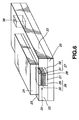
- the magnetic device shown here by way of illustration is a magnetic head.
- this magnetic head is constituted by a lower layer shield 20, a lower gap 21 formed on the lower layer shield 20, a magnetic tunnelling element 22 formed on the lower gap 21, an upper gap 23 formed on the magnetic tunnelling element 22, and an upper layer shield 24 formed on the upper gap 23.
- the magnetic head has its lateral side 25 as a facing surface to the magnetic recording medium and is designed so that the lower layer shield 20, magnetic tunnelling element 22, upper gap 23 and the upper layer shield 24 are exposed to this lateral side 25.
- the magnetic tunnelling element 2 is constructed so that a first magnetic metal layer 26 and a second magnetic metal layer 27 are layered together via a tunnel barrier layer 28 in-between.
- the first magnetic metal layer 26 is made up of a NiFe layer 29 and a Co layer 30, while the second magnetic metal layer 27 is made up of a Co film 31 and an IrMn film 32.
- the tunnel barrier layer 28 is formed by oxidizing the Al film by oxygen plasma generated by the high frequency induction coupling system.
- the lower gap 21 and the magnetic tunnelling element 22 are buried in an insulating layer 33 formed of an insulating material.
- the lower layer shield 20 and the upper layer shield 24 are formed of an electrically conductive magnetic material. By so doing, the lower layer shield 20 and the upper layer shield 24 are able to capture the magnetic field other than the signal magnetic field applied to the lateral side 25. Thus, it is possible with the present magnetic head to apply only the signal magnetic field to be reproduced to the magnetic tunnelling element 22.
- the lower gap 21 and the upper gap 23 are formed of an electrically conductive non-magnetic material.
- the first magnetic metal layer 26 can be magnetically isolated from the lower layer shield 20, while the second magnetic metal layer 27 can similarly be magnetically isolated from the upper layer shield 24. That is, with the lower gap 21, the magnetic tunnelling element 22 can be safeguarded against magnetic effects of the lower layer shield 20 formed of the magnetic material.
- the magnetic tunnelling element 22 can be safeguarded against magnetic effects of the upper layer shield 24 formed of the magnetic material.
- the lower layer shield 20, lower gap 21, upper gap 23 and the upper layer shield 24 are formed of an electrically conductive material, the lower layer shield 20 and the lower gap 21 prove an electrode for the first magnetic metal layer 26, whilst the upper gap 23 and the upper layer shield 24 prove an electrode for the second magnetic metal layer 27.
- the first magnetic metal layer 26 has a free magnetization film exhibiting uniaxial anisotropy in substantially the perpendicular direction to the signal magnetic field applied from the magnetic recording medium
- the second magnetic metal layer 27 has a fixed magnetization film having fixed magnetization in a direction substantially parallel to the signal magnetic field applied from the magnetic recording medium. If a predetermined signal magnetic field is applied to the magnetic head, the direction of magnetization of the free magnetization film is changed.
- the NiFe layer 29 and the Co film 31 represent a free magnetization film and a fixed magnetization film, respectively.
- the magnetic head there flows a constant current from the second magnetic metal layer 27 to the first magnetic metal layer 26. This causes the so-called tunnel current to flow between the second magnetic metal layer 27 and the first magnetic metal layer 26.
- the present magnetic head if the direction of magnetization of the free magnetization film (NiFe layer 29) of the first magnetic metal layer 26 is changed to change the relative angle between it and the direction of magnetization of the fixed magnetization film (Co film 31), the resistance value to the tunnel current is changed.
- the resistance value against the tunnel current can be measured by detecting the voltage of the constant current flowing between the second magnetic metal layer 27 and the first magnetic metal layer 26.
- the signal magnetic field from the magnetic recording medium can be detected by measuring changes in the resistance value to the tunnel current.
- the lower layer shield 20 formed of a magnetic material, such as sendust
- the lower gap 21 formed of a non-magnetic metal material, are formed on a major surface of a substrate 34 of, for example, AlTiC or TiO-CaO, commonly used for a thin-film magnetic head.
- the lower gap 21 proves the underground for the magnetic tunnelling element 22 and hence is desirably formed as a highly planar surface.
- NiFe layer 29, 18.8 nm in thickness, a Co film 30, 3.9 nm in thickness and an Al film, 1.3 nm in thickness, are formed in this order on the lower gap 21, as shown in Fig.8.
- the NiFe layer 29 and the Co film 30 are processed with orientation processing so as to have a uniaxial anisotropy in a substantially perpendicular direction with respect to the magnetic field applied from the magnetic recording medium.
- An Al film 35 then is oxidized in a chamber shown in Fig.3 with an oxygen plasma generated in accordance with the high frequency induction coupling system.
- the Al film is controlled in its oxidation by suitably adjusting e.g., the oxidation time, oxygen partial pressure, high frequency power or gas pressure.
- the forming processes for the above-mentioned respective films, oxidation processes for the Al film 35 and the film-forming processes, as later explained, are desirably carried out in the same chamber.
- the Co film 31 and the IrMn film 32 are formed in this order, as shown in Fig.9.
- the IrMn film 32 is processed with orientation processing so that an exchange coupling magnetic field will be generated between it and the Co film 31 in a direction substantially parallel to the magnetic field applied from the magnetic recording medium.
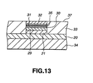
- a resist material is applied on the IrMn film 32 to form a resist film, which then is patterned by a photolithographic technique to form a resist pattern 36 of a predetermined shape, as shown in Fig.10. Specifically, the resist pattern 36 is patterned so that it will be left in an area which later proves the magnetic tunnelling element 22.
- the film is etched in an area not carrying the resist pattern 36, by a technique, such as Ar ion milling, until the lower layer shield 20 is exposed, as shown in Fig.11.
- a technique such as Ar ion milling
- the lower gap 21, NiFe layer 29, Co film 30, oxidized Al film 35, Co film 31, IrMn film 32 and the resist pattern 36 are left on the lower layer shield 20. That is, the magnetic tunnelling element 22 of a predetermined shape is formed below the resist pattern 36.
- the insulating layer 33 formed of an insulating material, such as Al 2 O 3 , is then formed on the lower layer shield 20 and on the resist pattern 36, exposed to outside, as the resist pattern 36 is still left over. This insulating layer 33 is formed on the lower layer shield 20 so that the insulating layer 33 will be at the same height level as the interface between the resist pattern 36 and the IrMn film 32.
- the resist pattern 36 and the insulating layer 33 formed thereon are detached by e.g., an organic solvent to planarize a major surface 37.
- the upper layer shield 24 may be formed by a plating method employing the resist pattern of the predetermined shape or by forming the upper layer shield 24 on the entire surface of the upper gap 23 by sputtering and subsequently etching the upper layer shield 24.
- the insulating layer 33, lower gap 21 and the lower layer shield 20 are formed to a predetermined shape by photolithography and etching and an opening 38 is bored in the insulating layer 33 to enable electric connection with the lower layer shield 20.
- An opening 38 is formed in the insulating layer 33 to expose the lower layer shield 20 via the opening 38.
- An electrically conductive material is charged into the opening 38, in a manner not shown, to enable electric connection of the lower layer shield 20.
- the Al film 35 is oxidized, using the oxygen plasma generated by the high frequency induction coupling system, to form the tunnel barrier layer 28.
- the tunnel current flows reliably across the first magnetic metal layer 26 and the second magnetic metal layer 27.
- the tunnel barrier layer 28 can be reliably formed by the above technique to prevent an inconvenience of the current flowing through the first magnetic metal layer 26 and the second magnetic metal layer 27 to improve the production yield at the time of manufacture of the magnetic head.
Landscapes
- Engineering & Computer Science (AREA)
- Chemical & Material Sciences (AREA)
- Nanotechnology (AREA)
- Physics & Mathematics (AREA)
- Crystallography & Structural Chemistry (AREA)
- Manufacturing & Machinery (AREA)
- Condensed Matter Physics & Semiconductors (AREA)
- General Physics & Mathematics (AREA)
- Mathematical Physics (AREA)
- Theoretical Computer Science (AREA)
- Hall/Mr Elements (AREA)
- Magnetic Heads (AREA)
Applications Claiming Priority (2)
| Application Number | Priority Date | Filing Date | Title |
|---|---|---|---|
| JP26369598 | 1998-09-17 | ||
| JP10263695A JP2000099922A (ja) | 1998-09-17 | 1998-09-17 | 磁気トンネル素子及びその製造方法 |
Publications (2)
| Publication Number | Publication Date |
|---|---|
| EP0987685A2 true EP0987685A2 (de) | 2000-03-22 |
| EP0987685A3 EP0987685A3 (de) | 2000-04-05 |
Family
ID=17393062
Family Applications (1)
| Application Number | Title | Priority Date | Filing Date |
|---|---|---|---|
| EP99118414A Withdrawn EP0987685A3 (de) | 1998-09-17 | 1999-09-16 | Element mit magnetischem Tunneleffekt und Verfahren zur dessen Herstellung |
Country Status (3)
| Country | Link |
|---|---|
| US (1) | US6519123B1 (de) |
| EP (1) | EP0987685A3 (de) |
| JP (1) | JP2000099922A (de) |
Cited By (1)
| Publication number | Priority date | Publication date | Assignee | Title |
|---|---|---|---|---|
| US6841395B2 (en) | 2002-11-25 | 2005-01-11 | International Business Machines Corporation | Method of forming a barrier layer of a tunneling magnetoresistive sensor |
Families Citing this family (20)
| Publication number | Priority date | Publication date | Assignee | Title |
|---|---|---|---|---|
| US6853520B2 (en) | 2000-09-05 | 2005-02-08 | Kabushiki Kaisha Toshiba | Magnetoresistance effect element |
| JP2002217030A (ja) * | 2001-01-23 | 2002-08-02 | Hitachi Ltd | 磁気抵抗効果磁気センサー及び磁気記録再生装置 |
| JP2003086866A (ja) * | 2001-09-13 | 2003-03-20 | Anelva Corp | スピンバルブ型巨大磁気抵抗薄膜の製造方法 |
| KR100465600B1 (ko) * | 2002-05-20 | 2005-01-13 | 주식회사 하이닉스반도체 | 엠.티.제이. 셀 및 그 제조방법 |
| JP4690675B2 (ja) * | 2004-07-30 | 2011-06-01 | 株式会社東芝 | 磁気抵抗効果素子、磁気ヘッド、および磁気記録再生装置 |
| US7595967B1 (en) * | 2004-09-07 | 2009-09-29 | Western Digital (Fremont), Llp | Method for fabricating a spacer layer for a magnetoresistive element |
| JP4521316B2 (ja) | 2005-05-26 | 2010-08-11 | 株式会社東芝 | 磁気抵抗効果素子、磁気ヘッド、および磁気記録再生装置 |
| JP4786331B2 (ja) | 2005-12-21 | 2011-10-05 | 株式会社東芝 | 磁気抵抗効果素子の製造方法 |
| JP4514721B2 (ja) * | 2006-02-09 | 2010-07-28 | 株式会社東芝 | 磁気抵抗効果素子の製造方法、磁気抵抗効果素子、磁気抵抗効果ヘッド、磁気記録再生装置及び磁気記憶装置 |
| JP2007299880A (ja) * | 2006-04-28 | 2007-11-15 | Toshiba Corp | 磁気抵抗効果素子,および磁気抵抗効果素子の製造方法 |
| JP4550777B2 (ja) | 2006-07-07 | 2010-09-22 | 株式会社東芝 | 磁気抵抗効果素子の製造方法、磁気抵抗効果素子、磁気ヘッド、磁気記録再生装置及び磁気メモリ |
| JP5044157B2 (ja) * | 2006-07-11 | 2012-10-10 | 株式会社東芝 | 磁気抵抗効果素子,磁気ヘッド,および磁気再生装置 |
| JP4764294B2 (ja) * | 2006-09-08 | 2011-08-31 | 株式会社東芝 | 磁気抵抗効果素子、及び磁気ヘッド |
| JP4388093B2 (ja) | 2007-03-27 | 2009-12-24 | 株式会社東芝 | 磁気抵抗効果素子、磁気ヘッド、磁気記録再生装置 |
| JP5039006B2 (ja) | 2008-09-26 | 2012-10-03 | 株式会社東芝 | 磁気抵抗効果素子の製造方法、磁気抵抗効果素子、磁気ヘッドアセンブリ及び磁気記録再生装置 |
| JP5039007B2 (ja) | 2008-09-26 | 2012-10-03 | 株式会社東芝 | 磁気抵抗効果素子の製造方法、磁気抵抗効果素子、磁気ヘッドアセンブリ及び磁気記録再生装置 |
| JP2010080839A (ja) | 2008-09-29 | 2010-04-08 | Toshiba Corp | 磁気抵抗効果素子の製造方法、磁気抵抗効果素子、磁気ヘッドアセンブリおよび磁気記録再生装置 |
| JP2009055050A (ja) * | 2008-10-06 | 2009-03-12 | Canon Anelva Corp | スピンバルブ型巨大磁気抵抗薄膜またはtmr膜の製造方法 |
| JP2009158089A (ja) * | 2009-04-06 | 2009-07-16 | Canon Anelva Corp | スピンバルブ型巨大磁気抵抗薄膜またはtmr膜の製造方法 |
| US11133029B2 (en) * | 2018-12-19 | 2021-09-28 | International Business Machines Corporation | Tape head with element-to-element spacing and adjustment and mechanism to control the spacing |
Citations (1)
| Publication number | Priority date | Publication date | Assignee | Title |
|---|---|---|---|---|
| EP0719874A1 (de) * | 1994-12-26 | 1996-07-03 | Shincron Co., Ltd. | Verfahren und Vorrichtung zur Herstellung dünner Schichten von metallischen Verbindungen |
Family Cites Families (6)
| Publication number | Priority date | Publication date | Assignee | Title |
|---|---|---|---|---|
| US4548834A (en) * | 1982-05-31 | 1985-10-22 | Nec Corporation | Method of producing a Josephson tunnel barrier |
| US5430355A (en) | 1993-07-30 | 1995-07-04 | Texas Instruments Incorporated | RF induction plasma source for plasma processing |
| US5764567A (en) | 1996-11-27 | 1998-06-09 | International Business Machines Corporation | Magnetic tunnel junction device with nonferromagnetic interface layer for improved magnetic field response |
| JP3279495B2 (ja) | 1997-02-06 | 2002-04-30 | 住友電気工業株式会社 | 光導波膜形成方法 |
| US5999379A (en) * | 1997-12-11 | 1999-12-07 | International Business Machines Corporation | Spin valve read head with plasma produced metal oxide insulation layer between lead and shield layers and method of making |
| US6125062A (en) * | 1998-08-26 | 2000-09-26 | Micron Technology, Inc. | Single electron MOSFET memory device and method |
-
1998
- 1998-09-17 JP JP10263695A patent/JP2000099922A/ja active Pending
-
1999
- 1999-09-09 US US09/392,554 patent/US6519123B1/en not_active Expired - Lifetime
- 1999-09-16 EP EP99118414A patent/EP0987685A3/de not_active Withdrawn
Patent Citations (1)
| Publication number | Priority date | Publication date | Assignee | Title |
|---|---|---|---|---|
| EP0719874A1 (de) * | 1994-12-26 | 1996-07-03 | Shincron Co., Ltd. | Verfahren und Vorrichtung zur Herstellung dünner Schichten von metallischen Verbindungen |
Cited By (1)
| Publication number | Priority date | Publication date | Assignee | Title |
|---|---|---|---|---|
| US6841395B2 (en) | 2002-11-25 | 2005-01-11 | International Business Machines Corporation | Method of forming a barrier layer of a tunneling magnetoresistive sensor |
Also Published As
| Publication number | Publication date |
|---|---|
| US6519123B1 (en) | 2003-02-11 |
| EP0987685A3 (de) | 2000-04-05 |
| JP2000099922A (ja) | 2000-04-07 |
Similar Documents
| Publication | Publication Date | Title |
|---|---|---|
| EP0987685A2 (de) | Element mit magnetischem Tunneleffekt und Verfahren zur dessen Herstellung | |
| US5946167A (en) | Magnetoresistive sensor having lead and/or bias layer structure contributing to a narrow gap | |
| US7810227B2 (en) | Process to manufacture CPP GMR read head | |
| US20040257721A1 (en) | Magnetic head using magneto-resistive effect and a manufacturing method thereof | |
| US20070188943A1 (en) | Magnetoresistance Effect Element, Method of Manufacturing Same and Magnetic Head Utilizing Same | |
| JPH11175920A (ja) | 磁気抵抗効果型複合ヘッドおよびその製造方法 | |
| US6972935B2 (en) | Current-in-plane magnetoresistive sensor with longitudinal biasing layer having a nonmagnetic oxide central region and method for fabrication of the sensor | |
| US6621666B2 (en) | Magnetoresistive-effect element having electrode layers oppositely disposed on main surfaces of a magnetoresistive-effect thin film having hard magnetic bias layers with a particular resistivity | |
| US6563682B1 (en) | Magneto resistive element | |
| US7068479B2 (en) | Magnetoresistance effect element comprising nano-contact portion not more than a fermi length, and magnetic head utilizing same | |
| JP3227128B2 (ja) | 薄膜導体層及び前記薄膜導体層を用いた磁気抵抗効果素子並びに薄膜導体層の製造方法 | |
| US7099124B2 (en) | Magnetoresistive-effect thin film, magnetoresistive-effect element, and magnetoresistive-effect magnetic head | |
| US7733611B2 (en) | Magnetoresistance effect element comprising nano-contact portion not more than a mean free path and magnetic head utilizing same | |
| US6118621A (en) | Magnetoresistance effect head having a pair of protrusions, steps or depressions between the detecting and nondetecting areas for improved off-track characteristics | |
| US20050068690A1 (en) | Magnetoresistance effect element and magnetic head | |
| US6452892B1 (en) | Magnetic tunnel device, method of manufacture thereof, and magnetic head | |
| JP4403337B2 (ja) | トンネル磁気抵抗効果素子、及びトンネル磁気抵抗効果型磁気ヘッド | |
| JP2000113421A (ja) | 磁気トンネル接合磁気抵抗ヘッド | |
| JP3050094B2 (ja) | スピンバルブ素子 | |
| JP2004079936A (ja) | 強磁性トンネル接合を有する積層膜、その製造方法、磁気センサ、磁気記録装置、及び、磁気メモリ装置 | |
| US6433969B1 (en) | Compound magnetoresistive head and method for manufacturing same | |
| US6350487B1 (en) | Spin-valve type thin film element and its manufacturing method | |
| US6787004B2 (en) | Method for manufacturing a spin valve film and a method of manufacturing a magnetoresistance-effect type magnetic head | |
| EP1098203A2 (de) | Bauteil mit magnetischem Tunnelkontakt, magnetoresistiver Kopf mit Tunneleffekt und Herstellungsverfahren | |
| JP2000076625A (ja) | 磁気抵抗効果素子および磁気抵抗効果素子の製造方法 |
Legal Events
| Date | Code | Title | Description |
|---|---|---|---|
| PUAI | Public reference made under article 153(3) epc to a published international application that has entered the european phase |
Free format text: ORIGINAL CODE: 0009012 |
|
| PUAL | Search report despatched |
Free format text: ORIGINAL CODE: 0009013 |
|
| AK | Designated contracting states |
Kind code of ref document: A2 Designated state(s): DE FR GB |
|
| AX | Request for extension of the european patent |
Free format text: AL;LT;LV;MK;RO;SI |
|
| RIC1 | Information provided on ipc code assigned before grant |
Free format text: 7G 11B 5/39 A, 7G 01R 33/09 B, 7H 01F 10/08 B |
|
| AK | Designated contracting states |
Kind code of ref document: A3 Designated state(s): AT BE CH CY DE DK ES FI FR GB GR IE IT LI LU MC NL PT SE |
|
| AX | Request for extension of the european patent |
Free format text: AL;LT;LV;MK;RO;SI |
|
| 17P | Request for examination filed |
Effective date: 20000906 |
|
| AKX | Designation fees paid |
Free format text: DE FR GB |
|
| 17Q | First examination report despatched |
Effective date: 20001130 |
|
| STAA | Information on the status of an ep patent application or granted ep patent |
Free format text: STATUS: THE APPLICATION IS DEEMED TO BE WITHDRAWN |
|
| 18D | Application deemed to be withdrawn |
Effective date: 20021129 |