EP0984320B1 - Information transmitting apparatus using flash light emission - Google Patents
Information transmitting apparatus using flash light emission Download PDFInfo
- Publication number
- EP0984320B1 EP0984320B1 EP99117140A EP99117140A EP0984320B1 EP 0984320 B1 EP0984320 B1 EP 0984320B1 EP 99117140 A EP99117140 A EP 99117140A EP 99117140 A EP99117140 A EP 99117140A EP 0984320 B1 EP0984320 B1 EP 0984320B1
- Authority
- EP
- European Patent Office
- Prior art keywords
- light emission
- signal
- flash
- transmitting apparatus
- information transmitting
- Prior art date
- Legal status (The legal status is an assumption and is not a legal conclusion. Google has not performed a legal analysis and makes no representation as to the accuracy of the status listed.)
- Expired - Lifetime
Links
- 238000004891 communication Methods 0.000 claims description 18
- 230000001360 synchronised effect Effects 0.000 claims description 2
- 239000003990 capacitor Substances 0.000 description 25
- 230000005540 biological transmission Effects 0.000 description 23
- 229910052724 xenon Inorganic materials 0.000 description 22
- FHNFHKCVQCLJFQ-UHFFFAOYSA-N xenon atom Chemical compound [Xe] FHNFHKCVQCLJFQ-UHFFFAOYSA-N 0.000 description 22
- 238000000034 method Methods 0.000 description 20
- 230000003287 optical effect Effects 0.000 description 6
- 238000012937 correction Methods 0.000 description 3
- 150000002500 ions Chemical class 0.000 description 2
- 238000012545 processing Methods 0.000 description 2
- 238000004804 winding Methods 0.000 description 2
- 230000003466 anti-cipated effect Effects 0.000 description 1
- 238000006243 chemical reaction Methods 0.000 description 1
- 238000010276 construction Methods 0.000 description 1
- 230000001934 delay Effects 0.000 description 1
- 230000003111 delayed effect Effects 0.000 description 1
- 238000001514 detection method Methods 0.000 description 1
- 238000010586 diagram Methods 0.000 description 1
- 238000012986 modification Methods 0.000 description 1
- 230000004048 modification Effects 0.000 description 1
- 238000012544 monitoring process Methods 0.000 description 1
- 238000009877 rendering Methods 0.000 description 1
- 230000008054 signal transmission Effects 0.000 description 1
Images

Classifications
-
- G—PHYSICS
- G03—PHOTOGRAPHY; CINEMATOGRAPHY; ANALOGOUS TECHNIQUES USING WAVES OTHER THAN OPTICAL WAVES; ELECTROGRAPHY; HOLOGRAPHY
- G03B—APPARATUS OR ARRANGEMENTS FOR TAKING PHOTOGRAPHS OR FOR PROJECTING OR VIEWING THEM; APPARATUS OR ARRANGEMENTS EMPLOYING ANALOGOUS TECHNIQUES USING WAVES OTHER THAN OPTICAL WAVES; ACCESSORIES THEREFOR
- G03B15/00—Special procedures for taking photographs; Apparatus therefor
- G03B15/02—Illuminating scene
- G03B15/03—Combinations of cameras with lighting apparatus; Flash units
- G03B15/05—Combinations of cameras with electronic flash apparatus; Electronic flash units
-
- G—PHYSICS
- G03—PHOTOGRAPHY; CINEMATOGRAPHY; ANALOGOUS TECHNIQUES USING WAVES OTHER THAN OPTICAL WAVES; ELECTROGRAPHY; HOLOGRAPHY
- G03B—APPARATUS OR ARRANGEMENTS FOR TAKING PHOTOGRAPHS OR FOR PROJECTING OR VIEWING THEM; APPARATUS OR ARRANGEMENTS EMPLOYING ANALOGOUS TECHNIQUES USING WAVES OTHER THAN OPTICAL WAVES; ACCESSORIES THEREFOR
- G03B17/00—Details of cameras or camera bodies; Accessories therefor
- G03B17/38—Releasing-devices separate from shutter
-
- H—ELECTRICITY
- H05—ELECTRIC TECHNIQUES NOT OTHERWISE PROVIDED FOR
- H05B—ELECTRIC HEATING; ELECTRIC LIGHT SOURCES NOT OTHERWISE PROVIDED FOR; CIRCUIT ARRANGEMENTS FOR ELECTRIC LIGHT SOURCES, IN GENERAL
- H05B41/00—Circuit arrangements or apparatus for igniting or operating discharge lamps
- H05B41/14—Circuit arrangements
- H05B41/30—Circuit arrangements in which the lamp is fed by pulses, e.g. flash lamp
- H05B41/32—Circuit arrangements in which the lamp is fed by pulses, e.g. flash lamp for single flash operation
-
- G—PHYSICS
- G03—PHOTOGRAPHY; CINEMATOGRAPHY; ANALOGOUS TECHNIQUES USING WAVES OTHER THAN OPTICAL WAVES; ELECTROGRAPHY; HOLOGRAPHY
- G03B—APPARATUS OR ARRANGEMENTS FOR TAKING PHOTOGRAPHS OR FOR PROJECTING OR VIEWING THEM; APPARATUS OR ARRANGEMENTS EMPLOYING ANALOGOUS TECHNIQUES USING WAVES OTHER THAN OPTICAL WAVES; ACCESSORIES THEREFOR
- G03B2215/00—Special procedures for taking photographs; Apparatus therefor
- G03B2215/05—Combinations of cameras with electronic flash units
Definitions
- the present invention relates to an information transmitting apparatus arranged to transmit information by using flash light emission.
- Typical examples of known information transmitting apparatuses arranged to transmit optical information include remote controllers of TV sets, video tape recorders and the like. These remote controllers are arranged to use an infrared-emitting diode (IRED) as a light emitting device.
- IRED infrared-emitting diode
- the infrared-emitting diode has a quick responsivity and is capable of accurately transmitting information at a high speed.
- a shortcoming of the infrared-emitting diode lies in that the light emission output thereof is small and can reach only a short distance of several meters.
- the reachable distance can be made longer by using a light emitting device having an intense light output.
- some apparatus was developed to use a flash light emission tube having a large amount of light output for the light emitting device.
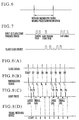
- a light release device disclosed in Japanese Laid-Open Utility Model Application No. SHO 55-99529 is arranged to control a shutter release action by emitting flash light from a signal transmitting side at intervals as shown in Fig. 6, and by receiving the flash light on the side of a photo-taking apparatus such as a camera or the like.
- a camera system disclosed in Japanese Laid-Open Patent Application No. HEI 4-343336 also uses a flash light emission tube as a light emitting device.
- This camera system is arranged, as shown in Fig. 7, to cause the flash light emission tube of a built-in flash light emission device of the camera to emit two control pulses at a predetermined interval and, upon lapse of a predetermined period of time after emission of the two control pulses, to emit one light emission start pulse for a slave flash device (a wireless flash device) in synchronism with the full open of the shutter.
- a slave flash device a wireless flash device
- the arrangement for using a flash light emission tube as a light emitting device is capable of emitting a light signal (the control pulses and the light emission start pulse shown in Fig. 7) which has light emission energy per pulse several hundred or several thousand times as much as the light emission energy of the conventional arrangement and can reach a very far distance.
- the flash device In a case where the flash device is caused to continuously emit light at time intervals of one hundred microseconds or thereabout, on the other hand, the ions of gas such as Xe (xenon) gas sealed in the flash light emission tube still remain in a sufficient quantity within the flash light emission tube.
- a trigger signal When a trigger signal is applied to the flash light emission tube under such a condition, light emission immediately begins.
- the time lag before actual light emission after application of a trigger signal is long in the case of a long interval between the first light emission or previous light emission and the next light emission, and is short while light emission is continuously made. Under such a condition, the intervals of light emission pulses become uneven to make accurate communication impossible.
- Figs. 8(A) to 8(D) show in a timing chart, by way of example, how accurate information communication is caused to become impossible by the delays, or time lags, of light emission from a flash light emission tube.
- Fig. 8(A) shows a synchronizing clock signal which is a reference signal to be used for conducting optical communication. An optical information signal is sent out at intervals which coincide with the synchronizing clock signal.
- Fig. 8(B) shows the information signal to be sent in synchronism with the synchronizing clock signal. For example, a signal of "10001111" is sent.
- reference symbol START denotes a signal which is added in front of information signal data transmitted to give information of the start of signal transmission to a signal receiving device.
- Fig. 8(C) shows light pulses actually emitted from the flash light emission tube when a trigger signal is applied to the flash light emission tube in synchronism with the information signal shown in Fig. 8(B).
- the first light pulse P1 synchronized with the START signal and the intermediate light pulse P3, each of which is emitted after the lapse of a long interval from the preceding light emission, lag and delay to a great extent from their corresponding parts of the information signal shown in Fig. 8(B).
- the light pulse P2 and the light pulses P4 to P6, each of which is emitted continuously from the preceding light emission do not show much lagging. Therefore, the intervals of light pulse emission become uneven.
- the signal receiving device since the signal receiving device is arranged to make checks for the presence or absence of the light pulses at intervals of a fixed period of time and only during a short period of time, after receipt of the light pulse P1 emitted in synchronism with the START signal, the information signal transmitted as "10001111" from the signal transmitting side would be received as "00001000" because only the light pulse P3 which is emitted after about the same extent of lag (delay) as the light pulse P1 can be recognized. Under such a condition, it is hardly possible to accurately conduct communication.
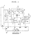
- Fig. 1 shows the circuit arrangement of an information transmitting apparatus according to the embodiment of the invention.
- a flash device is used as the information transmitting apparatus.
- reference numeral 1 denotes a known DC-DC converter (power supply means).
- a main capacitor 2 which is electric energy accumulating means is connected between the output terminals of the DC-DC converter 1.
- a series circuit which is composed of resistors 3 and 4 and is provided for detecting the output voltage of the DC-DC converter 1, is connected in parallel with the main capacitor 2.
- the emitter of a transistor 5 is connected to the positive terminal of the DC-DC converter 1.
- a resistor 6 is connected between the base and emitter of the transistor 5.
- a series circuit composed of resistors 8 and 9 is connected between the collector of the transistor 5 and the ground.
- the collector and emitter of a transistor 10 are connected between the juncture of the resistors 8 and 9 and the ground.
- a resistor 11 is connected between the base of the transistor 10 and the ground.
- One end of a resistor 12 is connected to the base of the transistor 10.
- One end of a voltage doubling capacitor 13 is connected to the collector of the transistor 5.
- a circuit which is formed by series-connecting a resistor 14, a capacitor 15 and the primary winding of a trigger transformer 16 is connected between the positive terminal of the DC-DC converter 1 and the ground.
- a coil 17 for controlling a light emission current is connected to the positive terminal of the DC-DC converter 1.
- a diode 18 is parallel-connected to the coil 17 in a direction opposite to the polarity of the output of the DC-DC converter 1.
- a diode 19 is connected to the output terminal of the coil 17 to have a forward output.
- the output terminal of the diode 19 is connected to one end of a xenon tube (flash light emission tube) 20.
- the trigger electrode of the xenon tube 20 is connected to the secondary winding of the trigger transformer 16.
- the other end of the xenon tube 20 is connected to other ends of the resistors 7 and 14 and the collector of an IGBT 21 (light emission control means).
- the emitter of the IGBT 21 is grounded.
- a resistor 22 is connected to the gate of the IGBT 21 and the ground.
- One end of a resistor 23 is connected to the gate of the IGBT 21.
- a series circuit composed of a photodiode 25 and a resistor 26 and another series circuit composed of resistors 27 and 28 are connected in parallel.
- Input terminals of a comparator 29 are connected respectively to the intermediate connection nodes of these parallel-connected series circuits.
- a microcomputer 30 which is arranged to control the whole information transmitting apparatus, there are connected the output terminal of the comparator 29, the terminal CNT of the DC-DC converter 1, the juncture of the resistors 3 and 4 and other ends of the resistors 12 and 23.
- a light emission amount control circuit is formed jointly by the reference voltage generating circuit 24, the photodiode 25, the comparator 29 and the circuits arranged around them.
- the microcomputer 30 is provided with terminals of varied kinds including terminals CNT, HV, QC, GATE and STOP. In addition to these terminals, the microcomputer 30 also has terminals X, DI, CHG, etc., connected to a connector 31 which is provided for connection with terminals provided on a camera (not shown).
- the DC-DC converter 1 is capable of controlling a charging action through the terminal CNT.
- the DC-DC converter 1 is arranged to boost the voltage of the power supply battery up to several hundred volts and to charge the main capacitor 2 with the voltage.
- the voltage of the main capacitor 2 is divided by the resistors 3 and 4 which are connected in parallel with the main capacitor 2.
- the voltage thus obtained is detected by the microcomputer 30.
- the microcomputer 30 controls the terminal CNT of the DC-DC converter 1 in such a way as to charge the main capacitor 2 with a voltage suited for light emission.
- a voltage doubling circuit for doubling the voltage of the main capacitor 2 is formed jointly by the transistor 5, the resistors 6 to 9, the transistor 20, the resistors 11 and 12 and the voltage doubling capacitor 13.
- a voltage which is obtained by adding the voltage of the voltage doubling capacitor 13 to the voltage of the main capacitor 2 is thus arranged to be applied to the xenon tube 20.
- the diode 18 is a flywheel diode which is arranged to absorb a voltage generated at the coil 17 when light emission is bought to a stop.
- the diode 19 is arranged to hold a voltage in such a way as to cause the doubled voltage applied from the voltage doubling capacitor 13 to be applied only to the anode of the xenon tube 20 at the time of light emission from the xenon tube 20.
- the connector 31 is provided for serial communication with the camera.
- the terminal CNT is an output terminal for control over the charging action of the DC-DC converter 1.
- the terminal HV is an analog-to-digital (A/D) conversion input terminal which is provided for monitoring the voltage of the main capacitor 2.
- the terminal QC is an output terminal for control over a charging action on the voltage doubling capacitor 13 to have the voltage doubling capacitor 13 quickly charged.
- the terminal GATE is an output terminal for control over the gate of the IGBT 21.
- the terminal STOP is an input terminal provided for inputting a light emission stop signal.
- the terminal X is an input terminal for inputting a light emission instruction signal from the camera.
- the terminal CLK is an input terminal for inputting a serial clock signal to be used for serial communication with the camera in a known manner.
- the terminal DI is a serial data input terminal.
- the terminal DO is a serial data output terminal.
- the terminal CHG is a current output terminal for transmitting information to the camera as to whether or not the light emission by the flash device can be made.
- the microcomputer 30 begins to constantly monitor the terminal voltage of the main capacitor 2 through the terminal HV. To make the voltage sufficient for light emission from the xenon tube 20, the microcomputer 30 causes the DC-DC converter 1 to act, through the terminal CNT, if the voltage is low, and stops the DC-DC converter 1 from acting if the voltage is high.
- the main capacitor 2 thus can be controlled to have a predetermined voltage.
- the microcomputer 30 When the voltage of the main capacitor 2 reaches a voltage level sufficient for light emission from the xenon tube 20, the microcomputer 30 causes a predetermined amount of current to flow from the terminal CHG to inform the camera (not shown) that information using the light emission has become communicable. Then, to transmit the information using the light emission through the information transmitting apparatus to a data receiving apparatus (not shown), the camera sends information on transmission data to the microcomputer 30 by known serial communication through the serial clock signal input terminal CLK, the serial data input terminal DI and the serial data output terminal DO.
- this information may include an amount of light emission, the mode of light emission such as flash light emission or a long-time light emission mode called the focal plane (FP) light emission, a length of time of light emission, or the like.
- this information may be any information that relates to a shutter speed, an aperture value, shutter release start timing, or the like.
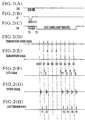
- Figs. 2(A) to 2(H) are timing charts showing the operation to be performed when the above-stated information is received from the camera.
- Reference symbol CLK in Fig. 2(A), reference symbol DI in Fig. 2(B) and reference symbol DO in Fig. 2(C) indicate known serial communication conducted between the camera and the microcomputer 30. Data is sent from the camera to the microcomputer 30 in synchronism with the synchronizing clock signal CLK through the terminal DI. In replay to the data, data is sent from the microcomputer 30 to the camera through the terminal DO.
- the serial communication begins at a point of time T0.
- Data to be transmitted (transmission data) is outputted from the camera to the terminal DI of the information transmitting apparatus, as shown in Fig. 2(B).
- the terminal DO is set at a low level to indicate that the information transmitting apparatus is in process of light emission.
- data "10001111" which indicates the timing of light emission, is assumed to be communicated from the microcomputer 30.
- the transmission timing signal is formed as a clock signal having a predetermined period within the microcomputer 30.
- the microcomputer 30 forms a transmission signal as shown in Fig. 2(E).
- the transmission signal is formed by adding a start bit indicative of the start of the optical communication to the transmission data. Data which follows the start bit is a signal for causing light emission when the data is "1" in accordance with the MSB first rule.
- the transmission signal shown in Fig. 2(E) is formed by adding the start bit to the above-stated data "10001111" sent to the microcomputer 30.
- the time lag (delay) of light emission from the xenon tube 20 causes the light emission pulses to be actually emitted to have uneven intervals between them (see Fig. 8(C)).
- the light emission start timing is corrected so as to make light emission intervals of the Xe tube 20 almost constant, by the steps of operation procedures described below with reference to Figs. 3 and 4, which are flow charts.
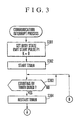
- a communication interruption takes place at the microcomputer 30.
- a communication interrupt process shown in Fig. 3 starts.
- the microcomputer 30 sets the terminal DO to a low level to indicate that the information transmitting apparatus is performing a process for light emission.
- the terminal GATE is set to a high level to generate a gate signal as shown in Fig. 2(F).
- the xenon tube 20 is then caused to emit a start pulse P1. This light emitting process will be described later with reference to the flow chart of Fig. 5.
- the microcomputer 30 sets the terminal GATE to a high level to execute a light emission process.
- the microcomputer 30 sets a light emission interval counter K set in a RAM (not shown) disposed within the microcomputer 30 to "0".
- a timer disposed within the microcomputer 30 to decide the light emission time of the next pulse is started.
- the flow of operation loops around the step S303 until arrival of the light emission time of the next pulse.
- the flow proceeds from the step S303 to a step S304.
- the timer is restarted, in the same manner as at the step S302, for the next light emission.
- the flow of operation proceeds from the step S304 of Fig.
- step S305 of Fig. 4 light emission data received from the camera is checked to find if the bit thereof currently received is "1" thus indicating that light emission is to be made this time. If so, the flow proceeds to a step S307. If not, i.e., if the bit of the light emission data is found to be "0", the flow proceeds from the step S305 to a step S306. At the step S306, "1" is added to the count value of the light emission interval counter K. The flow then proceeds from the step S306 to a step S311.
- the waiting time is set to be shorter accordingly as the time interval from the preceding light emission to the current light emission is longer, and the waiting time is set to be longer accordingly as the time interval from the preceding light emission to the current light emission is shorter.
- the microcomputer 30 causes each pulse of the gate signal to rise after the lapse of the waiting time obtained by referring to the "waiting time table" (Table 1) on the basis of the transmission signal (Fig. 2(E)). Then, the microcomputer 30 brings the light emission of the xenon tube 20 to a stop, by rendering the level of the terminal GATE low to cause each pulse of the gate signal to fall, either when the level of the terminal STOP is detected to have become low or after the . lapse of a predetermined period of time even if the terminal STOP is at a low level.
- a trigger signal shown in Fig. 2(G) is generated at the trigger transformer 16 with the IGBT 25 rendered conductive when the level of the terminal GATE becomes high, as will be described later.
- Fig. 2(H) shows light emission pulses generated by the xenon tube 20.
- step S311 a check is made to find if light emission for a predetermined number of bits has been completed. If not, the flow returns to the step S303 to repeat light emission processes until the last bit D0 is obtained. Upon completion of the light emission, the flow proceeds to a step S312. At the step S312, the light emission time measuring timer is stopped, and the busy state is canceled. The flow of light emission processes thus comes to an end.
- steps S305 to S307 which relate to the waiting time computing process, etc., are described as arranged, for simplifying the description, to be sequentially executed after the count of the timer is incremented. To eliminate the processing time lag, however, it is preferable to have a preparatory process executed for the next light emission before completion of time count by the timer at the step S303.
- the start pulse P1 emitted at the step S301 at the point of time D7 shown in Fig. 2(E) after the lapse of a predetermined time (the period of the transmission timing signal shown in Fig. 2(D)) for the steps S302 and S303, the light emission data is "1".
- the flow therefore, proceeds from the step S305 to the step S307.
- the lapse of the waiting time t4 of Table 1 corresponding to the value "0" of the counter K is awaited, and, after that, the light emission corresponding to the transmission signal is performed at the step S310 (the light emission for the pulse P2 is performed by setting the terminal GATE to the high level).
- the counter K is set to "0", and the flow returns to the step S303.
- the flow proceeds to the step S306.
- the flow then returns to the step S303 through the step S311. After that, these steps are repeated until data "1" is detected at a transmission point of time D3, i.e., until data D3(1) is detected. Since, in this instance, the step S306 is executed three times before detection of the data "1", the count value of the counter K becomes "3".
- the light emission for the pulse P3 is performed after the lapse of the time t1. Then, the counter K is set to "0", and the flow returns to the step S303. After that, since the data of each of the transmission points of time D2, D1 and D0 is "1", the light emission for each of the pulses P4, P5 and P6 is performed at the corresponding transmission point of time when the waiting time t4 lapses after the period of the transmission signal.
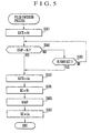
- the microcomputer 30 sets the terminal GATE to a high level. Then, the IGBT 21 becomes conductive. The electric charge in the trigger capacitor 15 flows through the collector and emitter of the IGBT 21 and the trigger transformer 16. A voltage of one thousand and several hundred volts is then generated on the secondary side of the trigger transformer 16. As a result, the xenon tube 20 is excited by this voltage and the discharge current of the xenon tube 20 flows through the IGBT 21, so that light emission from the xenon tube 20 begins. When the xenon tube 20 beings to emit light, the light is received by the photodiode 25 which is light receiving means. A current flows through the photodiode 25 according to the amount of light emission.
- a voltage corresponding to the amount of light emission is generated.
- This voltage of the resistor 26 becomes higher than a voltage obtained by the voltage division by the resistors 27 and 28.
- the output voltage of the comparator 29 is thus inverted from a low level to a high level.
- the microcomputer 30 makes a check to find if a voltage applied to the terminal STOP is at a high level. If so, the flow proceeds to a step S504 to bring the light emission of the xenon tube 20 to a stop. If not, the flow proceeds to a step S503.
- the flow proceeds from the step S503 to the step S504 to forcibly terminate the light emission, even when the level of the terminal STOP is low. If not, the flow returns to the step S502.
- the microcomputer 30 sets the terminal GATE to a low level. By this process, the IGBT 21 is turned off to cut off the light emission current of the xenon tube 20. Then, the light emission comes to a stop.
- the microcomputer 30 sets the terminal QC to a high level. The high level of the terminal QC renders the transistor 10 conductive to quickly charge the voltage doubling capacitor 13 only through the resistor 8.
- a waiting time (WAIT) before the light emission is set.
- WAIT waiting time
- the microcomputer 30 sets the terminal QC to a low level, so that the transistor 10 is turned off to bring the flow of pulse emitting processes to an end.
- the xenon tube 20 has a low impedance of only several ohms to bring the potential on the cathode side thereof up to about the same level as the potential on the anode side thereof.
- the trigger capacitor 15 is, therefore, automatically charged with a voltage thus obtained, so that preparation for the next light emission can be completed.
- the delay (lag) correction is arranged to be short when the light emission pulse interval is long, and is arranged to be long when the light emission pulse interval is short.
- the object of the invention can be likewise attained by arranging a negative lag correction time to be long to have light emission made earlier than the reference time, when the interval between the preceding light emission pulse and the current light emission pulse is long, and by arranging the negative lag correction timing to be short to have light emission made immediately before the reference time when the interval between the preceding light emission pulse and the current light emission pulse is short.
- the embodiment is arranged to count the time intervals between pulses.
- the arrangement may be changed to have predetermined transmission data decoded beforehand, and to make a schedule of light emission timing on the basis of information on the light emission pulse train.
- the timing of exciting and causing light emission by the light emission control means is corrected on the basis of the value of time count of the light emission intervals in such a way as to make the light emission intervals almost constant. Therefore, even in a case where lagging of the actual light emission signal with respect to the information signal is anticipated, the timing of excited light emission can be adequately corrected, so that the light emission pulse intervals can be prevented from becoming uneven, thereby ensuring accurate transmission of optical information.
- the timing of excited light emission is decided on the basis of the time intervals of light emission pulses, the intervals between the light emission pulses can be prevented from becoming uneven.
- the arrangement for causing the timing of excited light emission to be short when the light emission interval is long and to be long when the light emission interval is short makes the intervals of the light emission pulses constant, so that the intervals between the light emission pulses are prevented from becoming uneven.
Landscapes
- Physics & Mathematics (AREA)
- General Physics & Mathematics (AREA)
- Stroboscope Apparatuses (AREA)
- Optical Communication System (AREA)
- Discharge-Lamp Control Circuits And Pulse- Feed Circuits (AREA)
- Details Of Television Systems (AREA)
Applications Claiming Priority (2)
| Application Number | Priority Date | Filing Date | Title |
|---|---|---|---|
| JP26103598 | 1998-09-01 | ||
| JP26103598A JP4100774B2 (ja) | 1998-09-01 | 1998-09-01 | 光情報通信装置 |
Publications (2)
| Publication Number | Publication Date |
|---|---|
| EP0984320A1 EP0984320A1 (en) | 2000-03-08 |
| EP0984320B1 true EP0984320B1 (en) | 2004-10-27 |
Family
ID=17356157
Family Applications (1)
| Application Number | Title | Priority Date | Filing Date |
|---|---|---|---|
| EP99117140A Expired - Lifetime EP0984320B1 (en) | 1998-09-01 | 1999-08-31 | Information transmitting apparatus using flash light emission |
Country Status (4)
| Country | Link |
|---|---|
| US (1) | US6167199A (enExample) |
| EP (1) | EP0984320B1 (enExample) |
| JP (1) | JP4100774B2 (enExample) |
| DE (1) | DE69921408T2 (enExample) |
Cited By (1)
| Publication number | Priority date | Publication date | Assignee | Title |
|---|---|---|---|---|
| US8351774B2 (en) | 2002-11-26 | 2013-01-08 | Lab Partners Associates, Inc. | Wireless communication system and method for photographic flash synchronization |
Families Citing this family (18)
| Publication number | Priority date | Publication date | Assignee | Title |
|---|---|---|---|---|
| JP4656465B2 (ja) * | 2000-05-30 | 2011-03-23 | キヤノン株式会社 | 光情報送信装置および光情報通信システム |
| JP2002162671A (ja) * | 2000-11-27 | 2002-06-07 | Olympus Optical Co Ltd | 複数の撮影手段と光源の同期装置 |
| JP4872170B2 (ja) * | 2001-07-31 | 2012-02-08 | 株式会社ニコン | カメラシステム |
| JP4637520B2 (ja) * | 2004-07-14 | 2011-02-23 | 中国電力株式会社 | 同時処理システム |
| WO2007012041A2 (en) | 2005-07-20 | 2007-01-25 | Lab Partners Associates, Inc. | Wireless photographic communication system and method |
| JP4337814B2 (ja) * | 2005-12-27 | 2009-09-30 | 日本電気株式会社 | 可視光通信装置、可視光通信システム、可視光通信方法及び可視光通信プログラム |
| US7437063B2 (en) * | 2006-04-07 | 2008-10-14 | Lab Partners Associates, Inc. | Wireless camera flash synchronizer system and method |
| US7664387B2 (en) * | 2006-09-01 | 2010-02-16 | Nokia Corporation | Exposure time selection in a transmission apparatus with a camera |
| JP5220104B2 (ja) | 2007-05-29 | 2013-06-26 | ラブ・パートナーズ・アソシエイツ・インコーポレーテッド | カメラとワイヤレスデバイスとの間のホットシュー通信を維持するためのシステムおよび方法 |
| JP5184819B2 (ja) * | 2007-05-31 | 2013-04-17 | 日清紡ホールディングス株式会社 | ソーラシミュレータ |
| US8326136B1 (en) | 2009-02-12 | 2012-12-04 | Lab Partners Associates, Inc. | Systems and methods for communicating with a device using one or more camera body controls |
| US8326141B1 (en) | 2009-02-12 | 2012-12-04 | Lab Partners Associates, Inc. | Systems and methods for changing power states of a remote device using one or more camera body controls and a preset delay |
| US8718461B2 (en) | 2009-02-12 | 2014-05-06 | Lab Partners Associates, Inc. | Photographic synchronization optimization system and method |
| US8614766B1 (en) | 2009-02-12 | 2013-12-24 | Lab Partners Associates, Inc. | Systems and methods for controlling a power state of a remote device using camera body backlighting control signaling |
| EP2396699A4 (en) | 2009-02-12 | 2012-10-03 | Lab Partners Associates Inc | SYSTEM AND METHOD FOR EARLY PHOTOGRAPHIC SYNCHRONIZATION |
| US8600224B2 (en) | 2010-07-14 | 2013-12-03 | Lab Partners Associates, Inc. | Photographic wireless communication protocol system and method |
| US9690169B2 (en) | 2013-11-04 | 2017-06-27 | Lab Partners Associates, Inc. | Photographic lighting system and method |
| US11674865B2 (en) * | 2018-06-22 | 2023-06-13 | Danfoss Power Solutions Ii Technology A/S | System and method utilizing a light transfer protocol for sensor monitoring hose assembly degradation |
Family Cites Families (8)
| Publication number | Priority date | Publication date | Assignee | Title |
|---|---|---|---|---|
| JPS622597Y2 (enExample) * | 1975-01-27 | 1987-01-21 | ||
| JP3173043B2 (ja) * | 1991-05-20 | 2001-06-04 | ミノルタ株式会社 | ワイヤレスフラッシュ撮影可能なカメラシステム及びワイヤレスフラッシュ |
| US5384611A (en) * | 1991-05-20 | 1995-01-24 | Minolta Camera Kabushiki Kaisha | Camera system capable of wireless flash photographing |
| JPH0519336A (ja) * | 1991-07-16 | 1993-01-29 | Olympus Optical Co Ltd | リモートコントロール兼用ストロボ装置 |
| JP2587890Y2 (ja) * | 1992-11-10 | 1998-12-24 | 株式会社ニコン | 電子閃光装置 |
| US5446512A (en) * | 1992-12-18 | 1995-08-29 | Asahi Kogaku Kogyo Kabushiki Kaisha | Camera system having remote controller |
| JP3259447B2 (ja) * | 1993-06-29 | 2002-02-25 | 株式会社ニコン | 電子閃光制御システム |
| US6034486A (en) * | 1996-12-25 | 2000-03-07 | Canon Kabushiki Kaisha | Electronic flash device |
-
1998
- 1998-09-01 JP JP26103598A patent/JP4100774B2/ja not_active Expired - Fee Related
-
1999
- 1999-08-30 US US09/386,045 patent/US6167199A/en not_active Expired - Lifetime
- 1999-08-31 DE DE69921408T patent/DE69921408T2/de not_active Expired - Lifetime
- 1999-08-31 EP EP99117140A patent/EP0984320B1/en not_active Expired - Lifetime
Cited By (1)
| Publication number | Priority date | Publication date | Assignee | Title |
|---|---|---|---|---|
| US8351774B2 (en) | 2002-11-26 | 2013-01-08 | Lab Partners Associates, Inc. | Wireless communication system and method for photographic flash synchronization |
Also Published As
| Publication number | Publication date |
|---|---|
| DE69921408T2 (de) | 2006-02-02 |
| JP4100774B2 (ja) | 2008-06-11 |
| DE69921408D1 (de) | 2004-12-02 |
| JP2000078089A (ja) | 2000-03-14 |
| EP0984320A1 (en) | 2000-03-08 |
| US6167199A (en) | 2000-12-26 |
Similar Documents
| Publication | Publication Date | Title |
|---|---|---|
| EP0984320B1 (en) | Information transmitting apparatus using flash light emission | |
| GB2201052A (en) | Electronic flash | |
| JP2000047308A (ja) | カメラ付属品の取付検出装置 | |
| US9807853B2 (en) | Lighting device, lighting system, and external power source device | |
| US6828803B2 (en) | Strobe charge apparatus | |
| US6571061B2 (en) | Uniform flash-emission controller | |
| JP5340639B2 (ja) | キャパシタ充電装置およびその制御回路、制御方法、ならびにそれらを用いた発光装置および電子機器 | |
| US20020048457A1 (en) | Electric flash device and camera | |
| US6516153B2 (en) | Capacitor charging apparatus and electronic flash and apparatus containing same | |
| US4595267A (en) | Method of sending and receiving signals in photography with camera and camera flash device for that method | |
| CN119815626A (zh) | 闪光灯高速同步闪光的控制方法及控制系统 | |
| US4500190A (en) | Camera system including flash and status indicating control circuit | |
| CN117411305A (zh) | 一种多路错相功率因数校正电路、电源电路和显示设备 | |
| US4223367A (en) | Circuit for driving saw-tooth current in a coil | |
| JP4656465B2 (ja) | 光情報送信装置および光情報通信システム | |
| EP0851717B1 (en) | Electronic flash device | |
| JP2001209093A (ja) | カメラのストロボ制御装置 | |
| JP2017121029A (ja) | 制御装置、電子機器、および制御システム | |
| JP3338160B2 (ja) | フラッシュ光通信装置 | |
| JP2010237428A (ja) | 光情報通信装置、ストロボ装置および撮像装置 | |
| US4389596A (en) | Photometry power supply for automatic electronic flash | |
| JP2013162283A (ja) | 光情報通信装置、その制御方法、および制御プログラム | |
| JPS61156245A (ja) | カメラの受信確認装置 | |
| CN103167241A (zh) | 通信装置及其通信控制方法 | |
| JP2907287B2 (ja) | 閃光発光装置 |
Legal Events
| Date | Code | Title | Description |
|---|---|---|---|
| PUAI | Public reference made under article 153(3) epc to a published international application that has entered the european phase |
Free format text: ORIGINAL CODE: 0009012 |
|
| AK | Designated contracting states |
Kind code of ref document: A1 Designated state(s): DE FR GB |
|
| AX | Request for extension of the european patent |
Free format text: AL;LT;LV;MK;RO;SI |
|
| 17P | Request for examination filed |
Effective date: 20000720 |
|
| AKX | Designation fees paid |
Free format text: DE FR GB |
|
| GRAP | Despatch of communication of intention to grant a patent |
Free format text: ORIGINAL CODE: EPIDOSNIGR1 |
|
| GRAS | Grant fee paid |
Free format text: ORIGINAL CODE: EPIDOSNIGR3 |
|
| GRAA | (expected) grant |
Free format text: ORIGINAL CODE: 0009210 |
|
| AK | Designated contracting states |
Kind code of ref document: B1 Designated state(s): DE FR GB |
|
| REG | Reference to a national code |
Ref country code: GB Ref legal event code: FG4D |
|
| REF | Corresponds to: |
Ref document number: 69921408 Country of ref document: DE Date of ref document: 20041202 Kind code of ref document: P |
|
| PLBE | No opposition filed within time limit |
Free format text: ORIGINAL CODE: 0009261 |
|
| STAA | Information on the status of an ep patent application or granted ep patent |
Free format text: STATUS: NO OPPOSITION FILED WITHIN TIME LIMIT |
|
| ET | Fr: translation filed | ||
| 26N | No opposition filed |
Effective date: 20050728 |
|
| PGFP | Annual fee paid to national office [announced via postgrant information from national office to epo] |
Ref country code: FR Payment date: 20140827 Year of fee payment: 16 |
|
| REG | Reference to a national code |
Ref country code: FR Ref legal event code: ST Effective date: 20160429 |
|
| PG25 | Lapsed in a contracting state [announced via postgrant information from national office to epo] |
Ref country code: FR Free format text: LAPSE BECAUSE OF NON-PAYMENT OF DUE FEES Effective date: 20150831 |
|
| PGFP | Annual fee paid to national office [announced via postgrant information from national office to epo] |
Ref country code: GB Payment date: 20170830 Year of fee payment: 19 |
|
| PGFP | Annual fee paid to national office [announced via postgrant information from national office to epo] |
Ref country code: DE Payment date: 20171030 Year of fee payment: 19 |
|
| REG | Reference to a national code |
Ref country code: DE Ref legal event code: R119 Ref document number: 69921408 Country of ref document: DE |
|
| GBPC | Gb: european patent ceased through non-payment of renewal fee |
Effective date: 20180831 |
|
| PG25 | Lapsed in a contracting state [announced via postgrant information from national office to epo] |
Ref country code: DE Free format text: LAPSE BECAUSE OF NON-PAYMENT OF DUE FEES Effective date: 20190301 |
|
| PG25 | Lapsed in a contracting state [announced via postgrant information from national office to epo] |
Ref country code: GB Free format text: LAPSE BECAUSE OF NON-PAYMENT OF DUE FEES Effective date: 20180831 |