EP0981199A2 - Circuit électronique actif de filtrage - Google Patents
Circuit électronique actif de filtrage Download PDFInfo
- Publication number
- EP0981199A2 EP0981199A2 EP99202613A EP99202613A EP0981199A2 EP 0981199 A2 EP0981199 A2 EP 0981199A2 EP 99202613 A EP99202613 A EP 99202613A EP 99202613 A EP99202613 A EP 99202613A EP 0981199 A2 EP0981199 A2 EP 0981199A2
- Authority
- EP
- European Patent Office
- Prior art keywords
- filter
- input
- impedance
- amplifier
- active electronic
- Prior art date
- Legal status (The legal status is an assumption and is not a legal conclusion. Google has not performed a legal analysis and makes no representation as to the accuracy of the status listed.)
- Withdrawn
Links
Images
Classifications
-
- H—ELECTRICITY
- H03—ELECTRONIC CIRCUITRY
- H03H—IMPEDANCE NETWORKS, e.g. RESONANT CIRCUITS; RESONATORS
- H03H11/00—Networks using active elements
- H03H11/02—Multiple-port networks
- H03H11/04—Frequency selective two-port networks
- H03H11/12—Frequency selective two-port networks using amplifiers with feedback
- H03H11/126—Frequency selective two-port networks using amplifiers with feedback using a single operational amplifier
Definitions
- a tunable high-pass or low-pass filter is known from US Pat. No. 4,509,019, which comprises a push-pull amplifier, the electronically controllable elements either in the two input branches or the two feedback branches (or both in the input branches and the feedback branches). Is a reactance element each arranged in the other of the branches. This arrangement is said to be low Distortion can be achieved using a simple integration on a semiconductor body a nonlinear element, for example a MOS transistor, as voltage controllable element enables.
- this known filter circuit has the disadvantage that the Time constant that can be achieved with such a filter circuit, only over a relative low modulation range is adjustable, since the resistance values of the as controllable Elements used MOS transistors only over a comparatively small Control range can be varied.
- a filter arrangement is known from US Pat. No. 4,780,690, the time constant of which is about a comparatively wide range should be adjustable.
- This filter arrangement includes a push-pull amplifier that has an inverting input, a non-inverting Input, an inverting output, a non-inverting output, a first Input terminal and a second input terminal, a first feedback circuit, which comprises a first capacitor and between the non-inverting output and the inverting input is arranged, and a second feedback circuit, the comprises a second capacitor which is substantially identical to the first Capacitor and between the inverting output and the non-inverting Entrance is arranged contains.
- This known filter arrangement also contains one Transconductance circuit with variable transconductance, which comprises two inputs, the with are connected to the input connections of the filter arrangement, and two outputs which connected to the inverting and the non-inverting input of the amplifier are.
- a transconductance circuit is a voltage-controlled current source, through which a push-pull input voltage into a push-pull output current is converted. The proportionality factor between the output current and the The input voltage is determined by the transconductance. Generally can this transconductance can be varied over a comparatively wide range, whereby the time constant of the known filter arrangement over a comparative wide range should be able to be varied.
- the transconductance circuit according to the filter arrangement according to US Pat. No. 4,780,690 contains one A plurality of active elements, each of which has a control input and a first and has a second output terminal.
- the control inputs of at least two of the Active elements mentioned are with the input connections of the named Filter arrangement connected.
- the first output connections of the above, at least two active elements are directly connected to each other and the second output connections of these two active elements are the inverting and the non-inverting amplifier input connected.
- the filter arrangement known from US Pat. No. 4,780,690 also contains a load circuit for loading the transconductance circuit.
- This load circuit comprises a first and a second current source transistor, the interconnected base terminals of a diode connected to a junction of two resistors that are arranged between the outputs of the transconductance circuit.
- the invention has the task of an active electronic filter circuit To create input impedance arrangement with a high impedance value, which is based on a Semiconductor crystal with high accuracy and low consumption of crystal area can be made.
- the input impedance arrangement at least comprises a T-member with at least three impedance branches, a first of which Impedance branch with the filter input, a second impedance branch with the Amplifier input and a third impedance branch with a switching point Recording a current from the filter input is connected.
- a Provided impedance branch through which a part of the filter input or signal current supplied to the filter inputs at the associated amplifier input or on is routed past the associated amplifier inputs. This makes this part of the Signal current in the network determining the filter characteristic no further And the effective effective input impedance at the filter input or at the Filter inputs increase accordingly.
- a circuit point to include this Current from the filter input or the filter inputs can be a common of the circuit Serve ground connection.
- the input impedance arrangement comprises at least one T-member, in each of which a first, second, third or fourth Impedance branch with the first or second of the filter inputs or the first or second of the amplifier inputs is connected and the first and third impedance branches on the one hand with the second and fourth impedance branch on the other hand via a fifth Impedance branch are connected.
- Such an active electronic filter circuit is preferably used as a push-pull circuit a push-pull amplifier element. The is to the Part of the signal stream passed by amplifier inputs from one of the filter inputs derived to the other filter input via the fifth impedance branch, so that a separate circuit point for receiving this current is not required. Much more one of the filter inputs serves as such a node, and the Input impedance arrangement of the active electronic filter circuit in this Training can preferably be operated potential-free.
- the input impedance arrangement comprises at least two T-elements in Derailleur. With little circuitry, another important one can be created Achieve an increase in the impedance value of the input impedance arrangement.
- the T-link is or are the T-links constructed symmetrically with respect to the filter inputs and / or the amplifier inputs. This symmetrical structure is particularly indicated in push-pull circuits.
- the impedance branches are essentially formed from ohmic elements; in particular, at least some of the Controllable impedance branches, essentially include ohmic elements.
- the controllable, essentially ohmic elements within each T-member arranged symmetrically.
- controllable, essentially ohmic elements preferably formed with MOS transistors, the filter characteristic of the active electronic filter circuit according to the invention in an advantageous manner adjusted and precisely adjusted. When using MOS transistors this is possible in a manner known per se with control voltages.
- a preferred embodiment of an active electronic filter circuit according to the Invention represents the case that the network determining the filter characteristic as Integration stage - in cooperation with the amplifier element - is formed. At In such an integration stage, the input impedance arrangement is preferably purely ohmic educated.
- Active electronic filter circuits according to the invention are in all devices of the electronic communications technology can be used advantageously because of its integrability serve to miniaturize these devices on a semiconductor body. At the same time, yours Fiter characteristics can be set so precisely that a high quality of the Signal processing is achievable.
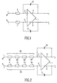
- the present invention is based on the example of a two-pole push-pull integrator filter are explained in more detail.
- Such an integrator filter is shown in FIG. 1.
- This integrator filter comprises an amplifier element 1 with a non-inverting amplifier input 2, one inverting amplifier input 3, an inverting amplifier output 4 and one non-inverting amplifier output 5.
- a the filter characteristic of the push-pull integrator filter determining network has an input impedance arrangement; the comprises a first ohmic resistor 6 and a second ohmic resistor 7.
- the first ohmic resistor 6 connects a first filter input 8 to the non-inverting amplifier input 2
- the second ohmic resistor 7 connects a second filter input 9 with the inverting amplifier input 3.
- the Filter characteristic of the push-pull integrator filter determining network further two capacities, a first one with the reference number 10 Feedback branch between the inverting amplifier output 4 and the forms non-inverting amplifier input 2, whereas the second capacitance 11 a feedback branch between the non-inverting amplifier output 5 and the inverting amplifier input 3 is formed.
- the amplifier outputs 4, 5 form also outputs of the push-pull integrator filter according to FIG. 1.
- a push-pull integrator filter When using controlled components, a push-pull integrator filter can be used as shown in FIG build with high precision, which also completely on one Semiconductor body can be integrated.
- regulated components i.e. in your Characteristic data controllable circuit elements, MOS transistors are preferred, with which the ohmic resistors 6, 7 can be built. This is basically known from US-PS 4,509,019.
- an active electronic filter circuit constructed in this way for example a push-pull integrator filter
- the procedure is in principle such that a so-called prototype filter from the specified specification for the filter to be created is developed.
- This is an ideal filter variant, in the present example an ideal variant of a push-pull integrator filter, implemented, with the assumption ideal Circuit elements.
- the input impedance arrangement comprises as the first or second ohmic resistor 60 or 70 each have a series connection of the shown in Example four resistance elements 61, 62, 63, 64 and 71, 72, 73, 74, each of which have a standardized value of the base resistance. So the first and the second ohmic resistance 60 or 70 in the exemplary embodiment according to FIG. 2 each four times Resistance value of a resistance element 61, 62, 63, 64, 71, 72, 73, or 74. For the Increasing the input contradiction fourfold is therefore a fourfold Circuitry required.
- This type of implementation is due to the large number of circuit elements that proportional to the desired resistance value in the input impedance arrangement increases, very expensive. It also increases with the number of circuit elements the number of parasitic capacitances effective therein, especially if the Resistor elements can be designed in the form of MOS transistors. Such Parasitic capacitances have a very negative effect on the desired filter characteristic especially in the higher frequency range. It is therefore a structure of the To strive for input impedance arrangement, which enables high resistance values with build up relatively few resistance elements.
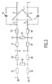
- FIG. 3 An exemplary embodiment of the solution to this problem according to the invention is shown in FIG. 3.
- the structure of the input impedance arrangement used in this filter circuit is based on the basic idea, the filter inputs 8, 9 currents supplied to the for the To pass filter characteristic effective amplifier inputs 2, 3 past. this will achieved in that the input impedance arrangement in the present Embodiment includes a T-member with five impedance branches.
- a first of these Impedance branches with the reference symbol 21 are on the one hand with the first filter input 8 and on the other hand connected to a first connection point 12.
- a second of the Impedance branches with the reference numeral 22 is between this first Connection point 12 and the non-inverting (first) amplifier input 2 arranged.
- a third of these impedance branches is identified by the reference symbol 23 between the second filter input 9 and a second connection point 13 arranged, of which via a fourth of the impedance branches with the reference numeral 24 there is a connection to the inverting (second) amplifier input 3.
- a fifth of the impedance branches with the Reference number 25 inserted is identified by the reference symbol 23 between the second filter input 9 and a second connection point 13 arranged, of which via a fourth of the impedance branches with the reference numeral 24 there is a connection to the inverting (second) amplifier input 3.
- Between two connection points 12, 13 is a fifth of the impedance branches with the Reference number 25 inserted.
- the input impedance arrangement formed in this way has a T-structure which ensures that part of a signal current flowing via the filter inputs 8, 9 is conducted past the virtual zero point of the amplifier element 1. As a result, this part of the signal current is not available for charging or discharging the capacitances 10, 11 and the effective input resistance of the push-pull integrator filter shown increases accordingly.
- the calculation of the effectively effective value for the input resistance at the filter inputs 8 and 9 with the aid of the network analysis yields the value of the ohmic resistance 6, 7, 60 and 70 for a filter circuit according to FIGS.
- the resistance elements 61 to 64 and 71 to 74 in FIG. 2 and the ohmic forming the impedance branches 21 to 25 of the T-element in FIG. 3 Dimensioned resistors with matching resistance values, it turns out that the effectively effective input resistances with respect to the filter inputs 8 and 9 in the 2 and 3 match filter circuits.
- three Opposing elements can be saved.
- the resistance values for the impedance branches 21 to 25 3 can also be used for others, in particular for higher effective effective resistance values of the input resistance with respect to the Filter inputs 8, 9 are dimensioned. It is advantageously possible to Impedance branches largely with the resistance value of the base resistance or less To multiply the same.
- the impedance branches 21 to 25 can then are at least largely composed of identical opposing elements. For some of the impedance branches 21 to 25, some dimensioning examples can be used from an integer multiple of the resistance value of the base resistor deviating resistance values become necessary, which, however, differ in their Distinguish dimensioning only relatively little from the base resistance.
- FIG. 3 An extension of the exemplary embodiment of the invention according to FIG. 3 is shown in broken lines there shown.
- This expansion includes a further T-link, each with a first, second, third, fourth and fifth impedance branches 31, 32, 33, 34 and 35 respectively the first T-link 21 to 25 is constructed.
- As filter inputs of the expanded Filter circuit serve connections 36 and 37.
- the further T-element 31 to 35 is to the first T-link 21 to 25 arranged in derailleur.
- the first, second, third and fourth can preferably be in the T-members Impedance branches as controllable, ohmic elements, preferably as MOS transistors, be trained. In particular, they can be controlled in pairs.
- the invention can also be based on asymmetrical Filter circuits are used.
- a simple example would be one Filter circuit with only one filter input, which is an amplifier element with only one Includes amplifier input and only one amplifier output.
- Integrator filter could be such a known filter circuit in a modification of FIG. 1 for example, only the first ohmic resistor 6 and the first capacitance 10 exhibit.
- the input impedance arrangement could have a first Impedance branch between the single filter input and a connection point, one second impedance branch between this connection point and the only one Amplifier input and a third impedance branch between the connection point and have mass. Part of the signal current supplied to the filter input is then derived to ground via the third impedance branch and reaches the Amplifier input not.
- filter circuits can also be used in addition to integrator filters other filter characteristics according to the invention.
- the difficulty in integrator filters can in particular be large values for the RC time constants to dimension with sufficient accuracy, on simple and dealt with effectively.
- With reduced circuitry and The smaller, required crystal surface is therefore a higher dimensioning accuracy and less influence of parasitic elements can be achieved.
Landscapes
- Networks Using Active Elements (AREA)
Applications Claiming Priority (2)
| Application Number | Priority Date | Filing Date | Title |
|---|---|---|---|
| DE19837574 | 1998-08-19 | ||
| DE19837574A DE19837574A1 (de) | 1998-08-19 | 1998-08-19 | Aktive elektronische Filterschaltung |
Publications (2)
| Publication Number | Publication Date |
|---|---|
| EP0981199A2 true EP0981199A2 (fr) | 2000-02-23 |
| EP0981199A3 EP0981199A3 (fr) | 2001-05-16 |
Family
ID=7877999
Family Applications (1)
| Application Number | Title | Priority Date | Filing Date |
|---|---|---|---|
| EP99202613A Withdrawn EP0981199A3 (fr) | 1998-08-19 | 1999-08-10 | Circuit électronique actif de filtrage |
Country Status (4)
| Country | Link |
|---|---|
| US (1) | US6255905B1 (fr) |
| EP (1) | EP0981199A3 (fr) |
| JP (1) | JP2000077976A (fr) |
| DE (1) | DE19837574A1 (fr) |
Families Citing this family (7)
| Publication number | Priority date | Publication date | Assignee | Title |
|---|---|---|---|---|
| US6897704B2 (en) * | 2001-05-25 | 2005-05-24 | Thunder Creative Technologies, Inc. | Electronic isolator |
| WO2006046294A1 (fr) * | 2004-10-28 | 2006-05-04 | Mitsubishi Denki Kabushiki Kaisha | Dispositif de linearisation |
| JP4755502B2 (ja) * | 2006-02-02 | 2011-08-24 | 日本オプネクスト株式会社 | 光受信機 |
| US20100127796A1 (en) * | 2006-03-22 | 2010-05-27 | C10 Communications Pty Ltd | Electronic filter and an electronic circuit for use in a switching application |
| JP2011158296A (ja) * | 2010-01-29 | 2011-08-18 | Asahi Kasei Electronics Co Ltd | π/2位相シフト回路、角速度検出回路 |
| CN102611411B (zh) * | 2011-12-20 | 2015-09-23 | 华为技术有限公司 | 一种跟踪补偿积分器、宽带滤波器及宽带模拟芯片 |
| US8970292B2 (en) | 2012-02-01 | 2015-03-03 | Texas Instruments Incorporated | Universal filter implementing second-order transfer function |
Citations (1)
| Publication number | Priority date | Publication date | Assignee | Title |
|---|---|---|---|---|
| US5424675A (en) * | 1992-05-29 | 1995-06-13 | Nec Corporation | Full differential type analog circuit having parallel oppositely connected capacitors to eliminate unbalanced parasitic capacitances |
Family Cites Families (5)
| Publication number | Priority date | Publication date | Assignee | Title |
|---|---|---|---|---|
| US3571761A (en) * | 1969-05-01 | 1971-03-23 | Hughues Aircraft Co | Transistorized amplitude modulation circuit with current control |
| US3715680A (en) * | 1971-07-29 | 1973-02-06 | Bell Telephone Labor Inc | Active rc loss equalizer |
| US4509019A (en) | 1983-01-27 | 1985-04-02 | At&T Bell Laboratories | Tunable active filter |
| NL8602894A (nl) | 1986-11-14 | 1988-06-01 | Philips Nv | Filterschakeling. |
| US5049831A (en) * | 1990-03-29 | 1991-09-17 | Motorola, Inc. | Single-ended input to differential output amplifier with integral two-pole filter |
-
1998
- 1998-08-19 DE DE19837574A patent/DE19837574A1/de not_active Withdrawn
-
1999
- 1999-08-10 EP EP99202613A patent/EP0981199A3/fr not_active Withdrawn
- 1999-08-16 US US09/374,693 patent/US6255905B1/en not_active Expired - Fee Related
- 1999-08-16 JP JP11229757A patent/JP2000077976A/ja active Pending
Patent Citations (1)
| Publication number | Priority date | Publication date | Assignee | Title |
|---|---|---|---|---|
| US5424675A (en) * | 1992-05-29 | 1995-06-13 | Nec Corporation | Full differential type analog circuit having parallel oppositely connected capacitors to eliminate unbalanced parasitic capacitances |
Non-Patent Citations (1)
| Title |
|---|
| BANU M ET TSIVIDIS Y: "AN ELLIPTIC CONTINUOUS-TIME CMOS FILTER WITH ON-CHIP AUTOMATIC TUNING" IEEE JOURNAL OF SOLID-STATE CIRCUITS, Bd. SC-20, Nr. 6, 1. - 1. Dezember 1985, Seiten 1114-1121, XP002163471 NEW YORK * |
Also Published As
| Publication number | Publication date |
|---|---|
| JP2000077976A (ja) | 2000-03-14 |
| EP0981199A3 (fr) | 2001-05-16 |
| US6255905B1 (en) | 2001-07-03 |
| DE19837574A1 (de) | 2000-02-24 |
Similar Documents
| Publication | Publication Date | Title |
|---|---|---|
| EP0559684B1 (fr) | Filtre universel | |
| DE69615300T2 (de) | Zeitkontinuierlich programmierbare analoge blockarchitektur | |
| DE68922139T2 (de) | Symmetrische Integratorfilterschaltungen. | |
| DE69727785T2 (de) | Filterschaltung | |
| DE69226862T2 (de) | Frequenzabstimmungssystem für ein Paar C-Transkonduktanzoperationsverstärker | |
| DE69222161T2 (de) | System zur Abstimmung eines Qualitätsfaktors | |
| EP0716783B1 (fr) | Etage amplificateur a tension de sortie lineaire en db | |
| DE3329820A1 (de) | Schaltungsanordnung mit einem gegenwirkleitwertelement | |
| DE3743603C2 (fr) | ||
| DE3309897C2 (fr) | ||
| EP0981199A2 (fr) | Circuit électronique actif de filtrage | |
| EP0755116B1 (fr) | Circuit pour le lissage d'une tension | |
| DE4213357C1 (en) | Wideband power amplifier using parallel transistors - has input circuit between successive input line sections and respective transistors for distributing input load | |
| DE4306511C2 (de) | Filterschaltung mit einem in Serienresonanz betriebenen Resonator | |
| DE3109375C2 (fr) | ||
| DE4306512C2 (de) | Filterschaltung mit einem in Serienresonanz betriebenen Resonator | |
| DE3323649C2 (de) | Schaltungsanordnung zur Erhöhung der Induktivität einer Spule | |
| DE69108424T2 (de) | Spannungsgesteuerter Widerstand. | |
| DE19628255C2 (de) | Filterschaltung | |
| DE2300285C3 (de) | Übertragungsnetzwerk | |
| EP0390076B1 (fr) | Filtre passe-bande pouvant être constitué sous forme de circuit intégré | |
| DE4101892C2 (fr) | ||
| DE2165745B1 (de) | Abstimmbarer Quarzoszillator | |
| DE1928515C3 (de) | Integrierbarer RC-Filtervierpol für Geräte und Einrichtungen der elektrischen Nachrichten-, MeB- und Datenverarbeitungstechnik | |
| DE3109375C3 (fr) |
Legal Events
| Date | Code | Title | Description |
|---|---|---|---|
| PUAI | Public reference made under article 153(3) epc to a published international application that has entered the european phase |
Free format text: ORIGINAL CODE: 0009012 |
|
| AK | Designated contracting states |
Kind code of ref document: A2 Designated state(s): DE FI FR GB IT |
|
| AX | Request for extension of the european patent |
Free format text: AL;LT;LV;MK;RO;SI |
|
| PUAL | Search report despatched |
Free format text: ORIGINAL CODE: 0009013 |
|
| AK | Designated contracting states |
Kind code of ref document: A3 Designated state(s): AT BE CH CY DE DK ES FI FR GB GR IE IT LI LU MC NL PT SE |
|
| AX | Request for extension of the european patent |
Free format text: AL;LT;LV;MK;RO;SI |
|
| 17P | Request for examination filed |
Effective date: 20011116 |
|
| STAA | Information on the status of an ep patent application or granted ep patent |
Free format text: STATUS: THE APPLICATION HAS BEEN WITHDRAWN |
|
| AKX | Designation fees paid |
Free format text: DE FI FR GB IT |
|
| 18W | Application withdrawn |
Withdrawal date: 20020125 |