EP0980113A2 - Antenne - Google Patents
Antenne Download PDFInfo
- Publication number
- EP0980113A2 EP0980113A2 EP99306272A EP99306272A EP0980113A2 EP 0980113 A2 EP0980113 A2 EP 0980113A2 EP 99306272 A EP99306272 A EP 99306272A EP 99306272 A EP99306272 A EP 99306272A EP 0980113 A2 EP0980113 A2 EP 0980113A2
- Authority
- EP
- European Patent Office
- Prior art keywords
- antenna
- conductor
- short
- circuited
- ground conductor
- Prior art date
- Legal status (The legal status is an assumption and is not a legal conclusion. Google has not performed a legal analysis and makes no representation as to the accuracy of the status listed.)
- Withdrawn
Links
Images


Classifications
-
- H—ELECTRICITY
- H01—ELECTRIC ELEMENTS
- H01Q—ANTENNAS, i.e. RADIO AERIALS
- H01Q13/00—Waveguide horns or mouths; Slot antennas; Leaky-waveguide antennas; Equivalent structures causing radiation along the transmission path of a guided wave
- H01Q13/08—Radiating ends of two-conductor microwave transmission lines, e.g. of coaxial lines, of microstrip lines
-
- H—ELECTRICITY
- H01—ELECTRIC ELEMENTS
- H01Q—ANTENNAS, i.e. RADIO AERIALS
- H01Q19/00—Combinations of primary active antenna elements and units with secondary devices, e.g. with quasi-optical devices, for giving the antenna a desired directional characteristic
- H01Q19/005—Patch antenna using one or more coplanar parasitic elements
-
- H—ELECTRICITY
- H01—ELECTRIC ELEMENTS
- H01Q—ANTENNAS, i.e. RADIO AERIALS
- H01Q1/00—Details of, or arrangements associated with, antennas
- H01Q1/12—Supports; Mounting means
- H01Q1/22—Supports; Mounting means by structural association with other equipment or articles
- H01Q1/24—Supports; Mounting means by structural association with other equipment or articles with receiving set
- H01Q1/241—Supports; Mounting means by structural association with other equipment or articles with receiving set used in mobile communications, e.g. GSM
- H01Q1/242—Supports; Mounting means by structural association with other equipment or articles with receiving set used in mobile communications, e.g. GSM specially adapted for hand-held use
- H01Q1/243—Supports; Mounting means by structural association with other equipment or articles with receiving set used in mobile communications, e.g. GSM specially adapted for hand-held use with built-in antennas
-
- H—ELECTRICITY
- H01—ELECTRIC ELEMENTS
- H01Q—ANTENNAS, i.e. RADIO AERIALS
- H01Q5/00—Arrangements for simultaneous operation of antennas on two or more different wavebands, e.g. dual-band or multi-band arrangements
- H01Q5/10—Resonant antennas
-
- H—ELECTRICITY
- H01—ELECTRIC ELEMENTS
- H01Q—ANTENNAS, i.e. RADIO AERIALS
- H01Q9/00—Electrically-short antennas having dimensions not more than twice the operating wavelength and consisting of conductive active radiating elements
- H01Q9/04—Resonant antennas
- H01Q9/0407—Substantially flat resonant element parallel to ground plane, e.g. patch antenna
- H01Q9/0421—Substantially flat resonant element parallel to ground plane, e.g. patch antenna with a shorting wall or a shorting pin at one end of the element
Definitions
- the present invention relates to an antenna device, and more particularly, is suitably applied to a portable telephone which is reduced in size.
- an antenna equipped in such a small portable radio apparatus is a micro-strip antenna (hereinafter referred to as the "MS antenna").
- MS antennas which are further reduced in size than the MS antennas, are a single-side short-circuited MS antenna having a short-circuit surface for short-circuiting a zero-potential surface at the center of a radiation conductor to a ground conductor, a laminar inverted-F antenna having a further reduced width of its short-circuit surface, and so on.
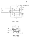
- a conventional MS antenna 1 comprises a ground conductor 2 disposed on one side of a dielectric substrate 3 having a height h , and a rectangular radiation conductor 4 (length a ⁇ width b ) formed on the other side of the substrate 3 using an etching technique or the like.
- This MS antenna 1 is provided with a power supply point 5 at a predetermined position on the radiation conductor 4 so that the input impedance thereof is equal to the characteristic impedance of a power supply system.
- the MS antenna 1 operates as an antenna with power supplied thereto through the power supply point 5.
- a single-side short-circuited MS antenna 6 comprises a short-circuit conductor 10 having a width Ws1 identical to the width b of a radiation conductor 8 and a height h , disposed between the radiation conductor 8 and a ground conductor 7, so as to short-circuit a zero-potential surface of the radiation conductor 8 to the ground conductor 7.
- the zero-potential surface, at which an electric field is at "0,” is at a position corresponding to one half a/2 of the length a of the radiation conductor 4 in the normal MS antenna 1.
- the single-side short-circuited MS antenna 6 only requires the radiation conductor 8 having a length dimension approximately one half of the length dimension of the radiation conductor 4 of the MS antenna 1, and still operates as an antenna at the same resonant frequency as the MS antenna 1.
- a laminar inverted-F antenna 10 is composed of a rectangular radiation conductor 12 (length c ⁇ width d ) and a ground conductor 11 which are short-circuited by a laminar inverted-F short-circuit conductor 14 having a width Ws2 smaller than the width Ws1 of the short-circuit conductor 10 of the single-side short-circuited MS antenna 6.
- the laminar inverted-F antenna 10 can reduce the resonant frequency fr by virtue of the laminar inverted-F short-circuit conductor 14 having the width Ws2 chosen to be smaller than the width Ws1 of the short-circuit conductor 8 of the single-side short-circuited MS antenna 6, and can further reduce the resonant frequency fr by virtue of the power supply point 5 defined at a position offset from the center line of the radiation conductor 12 by an offset amount Wx2, as compared with the power supply point 5 defined at the center of the radiation conductor 12.
- the laminar inverted-F antenna 10 is designed to reduce the resonant frequency fr more than the MS antenna 1, it can be configured using the radiation conductor 12 (length c ⁇ width d ) smaller than the radiation conductor 4 (length a ⁇ width b ), when it is operated at the same frequency as the MS antenna 1.
- the single-side short-circuited MS antenna 6 and the laminar inverted-F antenna 10, configured as described above, are required to be further reduced in size in response to the demand for increasingly smaller portable telephones in recent years.
- an object of this invention is to provide an antenna device which is capable of realizing a further reduction in size and weight.
- an antenna device which comprises a flat ground conductor; a first flat radiation conductor disposed against the flat ground conductor interposing a first dielectric layer; a first short-circuit conductor connecting an end of the first flat radiation conductor and the flat ground conductor; a second flat radiation conductor disposed partly against an opposite side of the first flat radiation conductor to its other side facing the ground conductor interposing a second dielectric layer; a second short-circuit conductor connecting an end of the second flat radiation conductor and the flat ground conductor; and a supply point disposed on the first flat radiation conductor.
- the first flat radiation conductor and the second flat radiation conductor are disposed partly against each other, which enables more size reduction than that of conventional antennas in operating at the same resonant frequency with a conventional antenna.
- a portable radio apparatus sends a voice signal S21 collected through a microphone 21 to an encoder circuit 22 upon transmission.
- the encoder circuit 22 encodes the voice signal S21 to generate audio data S22 which is sent to a modulator circuit 23.
- the modulator circuit 23 performs predetermined modulation processing based on the audio data S22 to generate a modulation signal S23 which is sent to a transmitter circuit 24.
- the transmitter circuit 24 digital-to-analog converts the modulation signal S23 to generate an analog signal which is then frequency converted to generate a transmission signal S25.
- the transmission signal S25 is amplified to a predetermined power level, and transmitted through a power supply line 25 and an external antenna 26 which comprises, for instance, an externally attached whip antenna.
- the portable radio apparatus 20 Upon reception, the portable radio apparatus 20 receives a reception signal S27 through the external antenna 26 and a planar antenna 27, and sends the reception signal S27 to a receiver circuit 27 through the power supply line 25 and a power supply line 28.
- the receiver circuit 29 amplifies the reception signal S29 to a predetermined power level, and then frequency converts the amplified signal to extract a baseband signal. Subsequently, the receiver circuit 29 analog-to-digital converts the baseband signal to a digital signal to generate a received data S29 which is sent to a demodulator circuit 30.
- the demodulator circuit 30 performs predetermined demodulation processing on the received data S29 to generate a demodulated signal S30 which is sent to a decoder circuit 31.
- the decoder circuit 31 decodes the demodulated signal S30 to generate an analog signal, thus recovering a voice signal S31 identical to an original voice signal 21 which is outputted through a speaker 32 as a voice.
- the portable radio apparatus 20 when in use, transmits a transmission signal S24 and receives a reception signal S27 with the external antenna 26 for both transmission and reception, which is drawn out from a housing 33 for use and otherwise can be retracted inside the housing 33.
- the portable radio apparatus 20 also receives the reception signal S27 through the planar antenna 27, implemented by the laminar inverted-F antenna 27 dedicated to reception which is always accommodated within the housing 33. In this way, the portable radio apparatus 20 conducts diversity reception, during reception, to improve the reception performance.
- the structure of the laminar inverted-F antenna 27, constituting the planar antenna 27, will be described in detail.
- a laminar inverted-F antenna according to the present invention, generally designated by 27.
- a radiation conductor 52 having a length (e-L) and a width f
- a ground conductor 51 having a width Ws2 and a height h , these to form a normal laminar inverted-F antenna.
- the laminar inverted-F antenna 27 is designed to act as a first antenna with a lower dielectric layer 56 formed of an air layer between the radiation conductor 52 and the ground conductor 51, as well as to act as a second antenna with an upper dielectric layer 55 formed of an air layer between the radiation conductor 52 and the upper ground conductor 53.
- the laminar inverted-F antenna 27 also has a power supply point 5 defined at a position spaced by a distance l from an end of the upper ground conductor 53 overlying the radiation conductor 52, and offset from the center line of the radiation conductor 52 by an offset amount Wx2, so that the input impedance of the radiation conductor 52 is equal to the characteristic impedance of a power supply system, thus achieving the impedance matching.
- the laminar inverted-F antenna device 27 has a first area S1 on one side of the radiation conductor 52 which acts as a first antenna in combination of the ground conductor 51 short-circuited by the laminar inverted-F short-circuit conductor 14, and an additional second area S2 on the other side of the radiation conductor 52 which acts as a second antenna in combination of the upper ground conductor 53 short-circuited by the side ground conductor 54.
- the laminar inverted-F antenna device 27 has an increased area (S1+S2), as a whole, for the radiation conductor 52, which acts as the overall antenna, resulting in a correspondingly increased capacitance to further reduce the resonant frequency fr.
- the second area S2 is reduced, resulting in a correspondingly reduced capacitance to increase the resonant frequency fr.
- the second area S2 is increased, resulting in a correspondingly increased capacitance to reduce the resonant frequency fr.
- the second area S2 is reduced, resulting in a correspondingly reduced capacitance to increase the resonant frequency fr.
- the second area S2 is increased, resulting in a correspondingly increased capacitance to reduce the resonant frequency fr.
- the laminar inverted-F antenna 27 can provide a desired resonant frequency by changing the length g of the upper ground conductor 53 and the length (e-L) of the radiation conductor 52 to adjust the area of the radiation conductor 52 which acts as the first and second antennas.
- the resonant frequency resulting from the use of the laminar inverted-F antenna 27 according to the present invention is at approximately 790MHz, whereas the resonant frequency resulting from the use of the conventional laminar inverted-F antenna 10 is at approximately 960MHz.
- the resonant frequency is significantly reduced by approximately 170 MHz.
- the laminar inverted-F antenna 27 employs a double-layer structure which includes a first antenna formed of a combination of the radiation conductor 52 and the ground conductor 51 short-circuited by the laminar inverted-F short-circuit conductor 14, and a second antenna formed of a combination of the radiation conductor 52 and the upper ground conductor 53 short-circuited by the side ground conductor 54.
- the first area S1 on the one side of the radiation conductor 52 acting as the first antenna and the second area S2 on the other side of the radiation conductor 52 acting as the second antenna are added to increase the area of the radiation conductor 52 acting as the overall antenna, so that the capacitance of the antenna can be increased as a whole.
- the laminar inverted-F antenna 27 can reduce the resonant frequency fr without causing increased dimensions (length e ⁇ width f ), as compared with the dimensions (length c ⁇ width d ) of the conventional laminar inverted-F antenna 10.
- the laminar inverted-F antenna 27 can further reduce the overall size thereof by an amount corresponding to a reduction in the resonant frequency fr, when operated at the same frequency as the conventional laminar inverted-F antenna 10, thereby making it possible to reduce the area of the antenna equipped in the portable radio apparatus 20 and hence the entire size of the portable radio apparatus 20.
- the laminar inverted-F antenna 27 employs the upper dielectric layer 55 and the lower dielectric layer 56 formed of air layers, the laminar inverted-F antenna 27 can be reduced in weight as compared with the conventional laminar inverted-F antenna 10 which employs the dielectric substrate 3.
- the laminar inverted-F antenna 27 in the first embodiment employs the double-layer structure which includes the first antenna formed of a combination of the radiation conductor 52 and the ground conductor 51 short-circuited by the laminar inverted-F short-circuit conductor 14, and the second antenna formed of a combination of the radiation conductor 52 and the upper ground conductor 53 short-circuited by the side ground conductor 54, thereby making it possible to further reduce the resonant frequency fr and the size of the overall antenna.
- a second embodiment has the same circuit configuration as the first embodiment except for a circuit associated with a laminar inverted-F antenna 60, later described, which is employed instead of the laminar inverted-F antenna 27 of the portable radio apparatus 20 (Fig. 4), description will be made herein only on the structure of the laminar inverted-F antenna 60.
- the laminar inverted-F antenna 60 comprises a side ground conductor 61 disposed on the side of an upper ground conductor 53 orthogonal to an open end side, on which a laminar inverted-F short-circuit conductor 14 is not disposed, so as to short-circuit the upper ground conductor 53 to a ground conductor 51 in place of the side ground conductor 54 of the laminar inverted-F antenna 27 in the first embodiment.
- a radiation conductor 62 has a width f', and is spaced apart from the side ground conductor 61 by a distance L' to avoid short-circuiting.
- the upper ground conductor 53 and the ground conductor 51 are short-circuited by the side ground conductor 61 in a manner similar to the laminar inverted-F antenna 27, so that a first antenna can be formed of a combination of the radiation conductor 62 and the ground conductor 51 short-circuited by the laminar inverted-F short-circuit conductor 14, and a second antenna can be formed of a combination of the radiation conductor 62 and the upper ground conductor 53 short-circuited by the side ground conductor 61.
- the first area S1 on one side of the radiation conductor 62 acting as the first antenna and the second area S2 on the other side of the radiation conductor 62 acting as the second antenna are added to increase the area of the radiation conductor 62 acting as the overall antenna, so that the capacitance of the antenna device can be increased. Consequently, the laminar inverted-F antenna 60 can reduce the resonant frequency fr without causing increased dimensions (length e ⁇ width f ), as compared with the dimensions (length c ⁇ width d ) of the conventional laminar inverted-F antenna 10.
- the laminar inverted-F antenna 60 can further reduce the overall size thereof by an amount corresponding to a reduction in the resonant frequency fr, when operated at the same frequency as the conventional laminar inverted-F antenna 10, thereby making it possible to reduce the area of the antenna equipped in the portable radio apparatus 20 and hence the entire size of the portable radio apparatus 20.
- the laminar inverted-F antenna 60 employs an upper dielectric layer 55 and a lower dielectric layer 56 formed of air layers, the laminar inverted-F antenna 60 can be reduced in weight as compared with the conventional laminar inverted-F antenna 10 which employs the dielectric substrate 3.
- the laminar inverted-F antenna 60 in the second embodiment employs the double-layer structure which includes the first antenna formed of a combination of the radiation conductor 62 and the ground conductor 51 short-circuited by the laminar inverted-F short-circuit conductor 14, and the second antenna formed of a combination of the radiation conductor 62 and the upper ground conductor 53 short-circuited by the side ground conductor 61, thereby making it possible to further reduce the resonant frequency fr and the size of the overall antenna.
- a third embodiment has the same circuit configuration as the first embodiment except for a circuit associated with a laminar inverted-F antenna 70, later described, which is employed instead of the laminar inverted-F antenna 27 of the portable radio apparatus 20 (Fig. 4), description will be made herein only on the structure of the laminar inverted-F antenna 70.
- the laminar inverted-F antenna 70 comprises both the side ground conductor 54 of the laminar inverted-F antenna 27 in the first embodiment, and the side ground conductor 61 of the laminar inverted-F antenna 60 in the second embodiment.
- an upper ground conductor 53 and a ground conductor 51 are short-circuited by the side ground conductors 54, 61 in a manner similar to the laminar inverted-F antennas 27, 60, so that a first antenna can be formed of a combination of a radiation conductor 62 and the ground conductor 51 short-circuited by the laminar inverted-F short-circuit conductor 14, and a second antenna can be formed of a combination of the radiation conductor 62 and the upper ground conductor 53 short-circuited by the side ground conductors 54, 61.
- the laminar inverted-F antenna 70 is such that a first area S1 on one side of the radiation conductor 62 acting as the first antenna and a second area S2 on the other side of the radiation conductor 62 acting as the second antenna are added to increase the area of the radiation conductor 62 acting as the overall antenna, so that the capacitance of the antenna can be increased as a whole. Consequently, the laminar inverted-F antenna 70 can reduce the resonant frequency fr without causing increased dimensions (length e ⁇ width f ), as compared with the dimensions (length c ⁇ width d ) of the conventional laminar inverted-F antenna 10.
- the laminar inverted-F antenna 70 can further reduce the overall size thereof by an amount corresponding to a reduction in the resonant frequency fr, when operated at the same frequency as the conventional laminar inverted-F antenna 10, thereby making it possible to reduce the area of the antenna equipped in the portable radio apparatus 20 and hence the entire size of the portable radio apparatus 20.
- the laminar inverted-F antenna 70 employs an upper dielectric layer 55 and a lower dielectric layer 56 formed of air layers, the laminar inverted-F antenna 70 can be reduced in weight as compared with the conventional laminar inverted-F antenna 10 which employs the dielectric substrate 3.
- the laminar inverted-F antenna 70 in the third embodiment employs the double-layer structure which includes the first antenna formed of a combination of the radiation conductor 62 and the ground conductor 51 short-circuited by the laminar inverted-F short-circuit conductor 14, and the second antenna formed of a combination of the radiation conductor 62 and the upper ground conductor 53 short-circuited by the side ground conductors 54, 61, thereby making it possible to further reduce the resonant frequency fr and the size of the overall antenna.
- a fourth embodiment has the same circuit configuration as the first embodiment except for a circuit associated with a single-side short-circuited MS antenna 80, later described, which is employed instead of the laminar inverted-F antenna 27 of the portable radio apparatus 20 (Fig. 4), description will be made herein only on the structure of the single-side short-circuited MS antenna 80.
- the single-side short-circuited MS antenna 80 comprises a radiation conductor 82 having a length (e-L) and a width f , and a ground conductor 81, short-circuited by a short-circuit conductor 10 having a width f and a height h to form a normal single-side short-circuited antenna.
- the antenna 80 also comprises an upper ground conductor 83 disposed at a position spaced from the radiation conductor 82 by a height h and having a length g and a width f , which is short-circuited to the ground conductor 81 by a side ground conductor 84 having a width f , which is disposed on an open end side on which the short-circuit conductor 10 is not disposed.
- the single-side short-circuited MS antenna 80 is designed to operate as a first antenna with a lower dielectric layer 86 formed of an air layer between the radiation conductor 82 and the ground conductor 81, as well as to operate as a second antenna with an upper dielectric layer 85 formed of an air layer between the radiation conductor 82 and the upper ground conductor 83.
- the single-side short-circuited MS antenna 80 also has a power supply point 5 defined at a position on the center line of the radiation conductor 82 spaced by a distance l from an end of the upper ground conductor 83 overlying the radiation conductor 82, so that the input impedance of the radiation conductor 82 is equal to the characteristic impedance of a power supply system, thus achieving the impedance matching.
- the single-side short-circuited MS antenna 80 has a first area S1 on one side of the radiation conductor 82 which acts as the first antenna in combination of the ground conductor 81 short-circuited by the short-circuit conductor 10, and an additional second area S2 on the other side of the radiation conductor 82 which acts as the second antenna in combination of the upper ground conductor 83 short-circuited by the side ground conductor 84.
- the single-side short-circuited MS antenna 80 has an increased area (S1+S2), as a whole, for the radiation conductor 82, which acts as the overall antenna, resulting in an increased capacitance to further reduce the resonant frequency fr.
- the second area S2 is reduced, resulting in a correspondingly reduced capacitance to increase the resonant frequency fr.
- the second area S2 is increased, resulting in a correspondingly increased capacitance to reduce the resonant frequency fr.
- the second area S2 is reduced, resulting in a correspondingly reduced capacitance to increase the resonant frequency fr.
- the second area S2 is increased, resulting in a correspondingly increased capacitance to reduce the resonant frequency fr.
- the single-side short-circuited MS antenna 80 can provide a desired resonant frequency by changing the length g of the upper ground conductor 83 and the length (e-L) of the radiation conductor 82 to adjust the area of the radiation conductor 82 which acts as the first and second antennas.
- the single-side short-circuited MS antenna 80 employs a double-layer structure which includes the first antenna formed of a combination of the radiation conductor 82 and the ground conductor 81 short-circuited by the short-circuit conductor 10, and the second antenna formed of a combination of the radiation conductor 82 and the upper ground conductor 83 short-circuited by the side ground conductor 84.
- the first area S1 on the one side of the radiation conductor 82 acting as the first antenna and the second area S2 on the other side of the radiation conductor 82 acting as the second antenna are added to increase the area of the radiation conductor 82 acting as the overall antenna, so that the capacitance of the antenna can be increased as a whole. Consequently, the single-side short-circuited MS antenna 80 can reduce the resonant frequency fr without causing increased dimensions (length e ⁇ width f ), as compared with those of the conventional single-side short-circuited MS antenna 6.
- the single-side short-circuited MS antenna 80 can further reduce the overall size thereof by an amount corresponding to a reduction in the resonant frequency fr, when operated at the same frequency as the conventional single-side short-circuited MS antenna 6, thereby making it possible to reduce the area of the antenna equipped in the portable radio apparatus 20 and hence the entire size of the portable radio apparatus 20.
- the single-side short-circuited MS antenna 80 employs the upper dielectric layer 85 and the lower dielectric layer 86 formed of air layers, the single-side short-circuited MS antenna 80 can be reduced in weight as compared with the conventional single-side short-circuited MS antenna 6 which employs the dielectric substrate 9.
- the single-side short-circuited MS antenna 80 in the fourth embodiment employs the double-layer structure which includes the first antenna formed of a combination of the radiation conductor 82 and the ground conductor 81 short-circuited by the short-circuit conductor 10, and the second antenna formed of a combination of the radiation conductor 82 and the upper ground conductor 83 short-circuited by the side ground conductor 84, thereby making it possible to further reduce the resonant frequency fr and the size of the overall antenna.
- a fifth embodiment has the same circuit configuration as the first embodiment except for a circuit associated with a single-side short-circuited MS antenna 90, later described, which is employed instead of the single-side short-circuited MS antenna 80 of the portable radio apparatus 20 (Fig. 4), description will be made herein only on the structure of the single-side short-circuited MS antenna 90.
- the single-side short-circuited MS antenna 90 comprises a side ground conductor 91 disposed on a side of an upper ground conductor 83 orthogonal to an open end side, on which a short-circuit conductor 10 is not disposed, so as to short-circuit the upper ground conductor 83 and a ground conductor 81, instead of the side ground conductor 84 of the single-side short-circuited MS antenna 80 in the fourth embodiment.
- a radiation conductor 92 has a width f' and is spaced apart from a side ground conductor 91 by a distance L' to avoid short-circuiting.
- the upper ground conductor 83 and the ground conductor 81 are short-circuited by the side ground conductor 91 in a manner similar to the single-side short-circuited MS antenna 80, so that a first antenna can be formed of a combination of the radiation conductor 92 and the ground conductor 81 short-circuited by the short-circuit conductor 10, and a second antenna can be formed of a combination of the radiation conductor 92 and the upper ground conductor 83 short-circuited by the side ground conductor 91.
- the single-side short-circuited MS antenna 90 is such that a first area S1 on one side of the radiation conductor 92 acting as the first antenna and a second area S2 on the other side of the radiation conductor 92 acting as the second antenna are added to increase the area of the radiation conductor 92 acting as the overall antenna, so that the capacitance of the antenna can be increased as a whole. Consequently, the single-side short-circuited MS antenna 90 can reduce the resonant frequency fr without causing increased dimensions (length e ⁇ width f ), as compared with those of the conventional single-side short-circuited MS antenna 6.
- the single-side short-circuited MS antenna 90 can further reduce the overall size thereof by an amount corresponding to a reduction in the resonant frequency fr, when operated at the same frequency as the conventional single-side short-circuited MS antenna 6, thereby making it possible to reduce the area of the antenna equipped in the portable radio apparatus 20 and hence the entire size of the portable radio apparatus 20.
- the single-side short-circuited MS antenna 90 employs an upper dielectric layer 85 and a lower dielectric layer 86 formed of air layers, the single-side short-circuited MS antenna 90 can be reduced in weight as compared with the conventional single-side short-circuited MS antenna 6 which employs the dielectric substrate 9.
- the single-side short-circuited MS antenna 90 in the fifth embodiment employs the double-layer structure which includes the first antenna formed of a combination of the radiation conductor 92 and the ground conductor 81 short-circuited by the short-circuit conductor 10, and the second antenna formed of a combination of the radiation conductor 92 and the upper ground conductor 83 short-circuited by the side ground conductor 91, thereby making it possible to further reduce the resonant frequency fr and the size of the overall antenna.
- a sixth embodiment has the same circuit configuration as the first embodiment except for a circuit associated with a single-side short-circuited MS antenna 100, later described, which is employed instead of the single-side short-circuited MS antenna 80 of the portable radio apparatus 20 (Fig. 4), description will be made herein only on the structure of the single-side short-circuited MS antenna 100.
- the single-side short-circuited MS antenna 100 comprises both the side ground conductor 84 of the single-side short-circuited MS antenna 80 in the fourth embodiment, and the side ground conductor 91 of the single-side short-circuited MS antenna 90 in the fifth embodiment.
- an upper ground conductor 83 and a ground conductor 81 are short-circuited by the side ground conductors 84, 91 in a manner similar to the single-side short-circuited MS antennas 80, 90, so that a first antenna can be formed of a combination of a radiation conductor 92 and the ground conductor 81 short-circuited by a short-circuit conductor 10, and a second antenna can be formed of a combination of the radiation conductor 92 and the upper ground conductor 83 short-circuited by the side ground conductors 84, 91.
- the single-side short-circuited MS antenna 100 is such that a first area S1 on one side of the radiation conductor 92 acting as the first antenna and a second area S2 on the other side of the radiation conductor 92 acting as the second antenna are added to increase the area of the radiation conductor 92 acting as the overall antenna, so that the capacitance of the antenna can be increased as a whole. Consequently, the single-side short-circuited MS antenna 100 can reduce the resonant frequency fr without causing increased dimensions (length e ⁇ width f ), as compared with those of the conventional single-side short-circuited MS antenna 6.
- the single-side short-circuited MS antenna 100 can further reduce the overall size thereof by an amount corresponding to a reduction in the resonant frequency fr, when operated at the same frequency as the conventional single-side short-circuited MS antenna 6, thereby making it possible to reduce the area of the antenna equipped in the portable radio apparatus 20 and hence the entire size of the portable radio apparatus 20.
- the single-side short-circuited MS antenna 100 employs an upper dielectric layer 85 and a lower dielectric layer 86 formed of air layers, the single-side short-circuited MS antenna 100 can be reduced in weight as compared with the conventional single-side short-circuited MS antenna 6 which employs the dielectric substrate 9.
- the single-side short-circuited MS antenna 100 in the sixth embodiment employs the double-layer structure which includes the first antenna formed of a combination of the radiation conductor 92 and the ground conductor 81 short-circuited by the short-circuit conductor 10, and the second antenna formed of a combination of the radiation conductor 92 and the upper ground conductor 83 short-circuited by the side ground conductors 84, 91, thereby making it possible to further reduce the resonant frequency fr and the size of the overall antenna.
- the present invention is not limited to such particular dielectric layers as disclosed.
- a laminar inverted-F antenna 110 illustrated in Figs. 13A and 13B a dielectric substrate 111 having a predetermined width Ws3 and a height h and made, for example, of glass fiber can be used instead of the upper dielectric layer 55.
- a variety of other materials can also be used for the dielectric substrate 111 other than glass fiber.
- the resonant frequency can be manipulated by adjusting the predetermined width Ws3 of the dielectric substrate 111.
- the present invention is not limited to such particular dielectric layers as disclosed.
- a dielectric substrate 121 having a predetermined width Ws4 and a height h and made, for example, of glass fiber can be used instead of the upper dielectric layer 85.
- a variety of other materials can also be used for the dielectric substrate 121 other than glass fiber.
- the resonant frequency can be manipulated by adjusting the predetermined width Ws4 of the dielectric substrate 121.
- the present invention is not limited to such a structure.
- the upper dielectric layer and the lower dielectric layer can be integrally formed.
- the upper ground conductor 53 or 83 and the ground conductor 51 or 81 are short-circuited by the side ground conductor 54, 61, 84 or 91.
- the present invention is not limited to such a structure, and in the alternative, the upper ground conductor and the ground conductor can be formed by bending an integrated conductor.
- the antenna device according to the present invention is applied to laminar inverted-F antennas and single-side short-circuited MS antennas.
- the present invention is not limited to these particular types of antennas, but can be applied to a variety of other planar antennas which exhibit a varying resonant frequency depending on the area of a radiation conductor.
Landscapes
- Engineering & Computer Science (AREA)
- Computer Networks & Wireless Communication (AREA)
- Waveguide Aerials (AREA)
- Variable-Direction Aerials And Aerial Arrays (AREA)
- Transceivers (AREA)
Applications Claiming Priority (2)
| Application Number | Priority Date | Filing Date | Title |
|---|---|---|---|
| JP10226341A JP2000059132A (ja) | 1998-08-10 | 1998-08-10 | アンテナ装置及び携帯無線機 |
| JP22634198 | 1998-08-10 |
Publications (2)
| Publication Number | Publication Date |
|---|---|
| EP0980113A2 true EP0980113A2 (de) | 2000-02-16 |
| EP0980113A3 EP0980113A3 (de) | 2001-03-07 |
Family
ID=16843660
Family Applications (1)
| Application Number | Title | Priority Date | Filing Date |
|---|---|---|---|
| EP99306272A Withdrawn EP0980113A3 (de) | 1998-08-10 | 1999-08-06 | Antenne |
Country Status (5)
| Country | Link |
|---|---|
| US (1) | US6229485B1 (de) |
| EP (1) | EP0980113A3 (de) |
| JP (1) | JP2000059132A (de) |
| KR (1) | KR20000017083A (de) |
| CN (1) | CN1244737A (de) |
Cited By (4)
| Publication number | Priority date | Publication date | Assignee | Title |
|---|---|---|---|---|
| EP1148581A1 (de) * | 2000-04-17 | 2001-10-24 | Kosan I & T Co., Ltd. | Mikrostreifenleiterantenne |
| GB2363002A (en) * | 2000-03-07 | 2001-12-05 | Nec Corp | Portable wireless unit including an antenna formed from two plane antennae |
| WO2002039547A1 (de) * | 2000-11-07 | 2002-05-16 | Siemens Aktiengesellschaft | Inverted-f-antenne |
| FR2825517A1 (fr) * | 2001-06-01 | 2002-12-06 | Socapex Amphenol | Antenne a plaque |
Families Citing this family (9)
| Publication number | Priority date | Publication date | Assignee | Title |
|---|---|---|---|---|
| JP2001257522A (ja) * | 2000-03-09 | 2001-09-21 | Sony Corp | アンテナ装置及び携帯無線機 |
| JP3640595B2 (ja) | 2000-05-18 | 2005-04-20 | シャープ株式会社 | 積層パターンアンテナ及びそれを備えた無線通信装置 |
| JP3630622B2 (ja) | 2000-08-31 | 2005-03-16 | シャープ株式会社 | パターンアンテナ及びそれを備えた無線通信装置 |
| US6943730B2 (en) * | 2002-04-25 | 2005-09-13 | Ethertronics Inc. | Low-profile, multi-frequency, multi-band, capacitively loaded magnetic dipole antenna |
| TW563274B (en) * | 2002-10-08 | 2003-11-21 | Wistron Neweb Corp | Dual-band antenna |
| GB2396484A (en) * | 2002-12-19 | 2004-06-23 | Nokia Corp | Reducing coupling between different antennas |
| JP4108660B2 (ja) * | 2004-09-15 | 2008-06-25 | Necアクセステクニカ株式会社 | 携帯電話機 |
| US8108517B2 (en) * | 2007-11-27 | 2012-01-31 | Umber Systems | System and method for collecting, reporting and analyzing data on application-level activity and other user information on a mobile data network |
| KR200482416Y1 (ko) | 2012-09-11 | 2017-01-20 | 대우조선해양 주식회사 | 선박엔진 벤트라인의 플러싱 기구 |
Family Cites Families (5)
| Publication number | Priority date | Publication date | Assignee | Title |
|---|---|---|---|---|
| US4749996A (en) * | 1983-08-29 | 1988-06-07 | Allied-Signal Inc. | Double tuned, coupled microstrip antenna |
| US5041838A (en) * | 1990-03-06 | 1991-08-20 | Liimatainen William J | Cellular telephone antenna |
| US5307075A (en) * | 1991-12-12 | 1994-04-26 | Allen Telecom Group, Inc. | Directional microstrip antenna with stacked planar elements |
| JPH08222940A (ja) * | 1995-02-14 | 1996-08-30 | Mitsubishi Electric Corp | アンテナ装置 |
| SE507077C2 (sv) * | 1996-05-17 | 1998-03-23 | Allgon Ab | Antennanordning för en portabel radiokommunikationsanordning |
-
1998
- 1998-08-10 JP JP10226341A patent/JP2000059132A/ja not_active Abandoned
-
1999
- 1999-08-04 KR KR1019990031987A patent/KR20000017083A/ko not_active Withdrawn
- 1999-08-06 EP EP99306272A patent/EP0980113A3/de not_active Withdrawn
- 1999-08-09 US US09/370,176 patent/US6229485B1/en not_active Expired - Fee Related
- 1999-08-10 CN CN99117787A patent/CN1244737A/zh active Pending
Cited By (6)
| Publication number | Priority date | Publication date | Assignee | Title |
|---|---|---|---|---|
| GB2363002A (en) * | 2000-03-07 | 2001-12-05 | Nec Corp | Portable wireless unit including an antenna formed from two plane antennae |
| GB2363002B (en) * | 2000-03-07 | 2002-09-11 | Nec Corp | Portable wireless unit |
| US6856819B2 (en) | 2000-03-07 | 2005-02-15 | Nec Corporation | Portable wireless unit |
| EP1148581A1 (de) * | 2000-04-17 | 2001-10-24 | Kosan I & T Co., Ltd. | Mikrostreifenleiterantenne |
| WO2002039547A1 (de) * | 2000-11-07 | 2002-05-16 | Siemens Aktiengesellschaft | Inverted-f-antenne |
| FR2825517A1 (fr) * | 2001-06-01 | 2002-12-06 | Socapex Amphenol | Antenne a plaque |
Also Published As
| Publication number | Publication date |
|---|---|
| EP0980113A3 (de) | 2001-03-07 |
| US6229485B1 (en) | 2001-05-08 |
| CN1244737A (zh) | 2000-02-16 |
| JP2000059132A (ja) | 2000-02-25 |
| KR20000017083A (ko) | 2000-03-25 |
Similar Documents
| Publication | Publication Date | Title |
|---|---|---|
| JP4301034B2 (ja) | アンテナが搭載された無線装置 | |
| US6268831B1 (en) | Inverted-f antennas with multiple planar radiating elements and wireless communicators incorporating same | |
| US6204819B1 (en) | Convertible loop/inverted-f antennas and wireless communicators incorporating the same | |
| US6529749B1 (en) | Convertible dipole/inverted-F antennas and wireless communicators incorporating the same | |
| CN101443957B (zh) | 用于无线通信的改进倒f形天线 | |
| EP1263079B1 (de) | Antenne für mobiles Telefon | |
| US6774849B2 (en) | Invented-F plate antenna and wireless communication device | |
| JPH11243318A (ja) | アンテナ | |
| US6229485B1 (en) | Antenna device | |
| KR20010075231A (ko) | 용량성으로 튜닝된 광대역 안테나 구조 | |
| EP1012904A4 (de) | Auf glas montierte zweibandantenne und flexibles gehäuse dafür | |
| JP3430140B2 (ja) | 逆fアンテナおよびそれを用いた無線装置 | |
| JP2003505964A (ja) | 無線通信機のための折りたたみデュアル周波数バンドアンテナ | |
| US8155607B2 (en) | Antenna apparatus of portable terminal | |
| US20030058168A1 (en) | Multi-frequency band inverted-F antennas with coupled branches and wireless communicators incorporating same | |
| CN1210837C (zh) | 细长形个人通信设备 | |
| JP2005526434A (ja) | アレイアプリケーションのアンテナ | |
| US6753818B2 (en) | Concealed antenna for mobile communication device | |
| JP2003101340A (ja) | ダイバーシティアンテナ及び無線通信装置 | |
| JPS6048626A (ja) | 携帯無線機 | |
| JP2005094499A (ja) | アンテナ装置、アンテナ素子製造方法及び通信装置 | |
| US6697021B2 (en) | Double F antenna | |
| US7193580B2 (en) | Antenna device | |
| JP3113460B2 (ja) | 移動体通信装置 | |
| JPH01222502A (ja) | 移動通信端末 |
Legal Events
| Date | Code | Title | Description |
|---|---|---|---|
| PUAI | Public reference made under article 153(3) epc to a published international application that has entered the european phase |
Free format text: ORIGINAL CODE: 0009012 |
|
| AK | Designated contracting states |
Kind code of ref document: A2 Designated state(s): DE FR GB |
|
| AX | Request for extension of the european patent |
Free format text: AL;LT;LV;MK;RO;SI |
|
| PUAL | Search report despatched |
Free format text: ORIGINAL CODE: 0009013 |
|
| AK | Designated contracting states |
Kind code of ref document: A3 Designated state(s): AT BE CH CY DE DK ES FI FR GB GR IE IT LI LU MC NL PT SE |
|
| AX | Request for extension of the european patent |
Free format text: AL;LT;LV;MK;RO;SI |
|
| 17P | Request for examination filed |
Effective date: 20010810 |
|
| AKX | Designation fees paid |
Free format text: DE FR GB |
|
| STAA | Information on the status of an ep patent application or granted ep patent |
Free format text: STATUS: THE APPLICATION HAS BEEN WITHDRAWN |
|
| 18W | Application withdrawn |
Withdrawal date: 20020314 |