EP0975979B1 - Verfahren zur herstellung von karten mit mehreren kontaktspitzen zum testen von halbleiterchips - Google Patents
Verfahren zur herstellung von karten mit mehreren kontaktspitzen zum testen von halbleiterchips Download PDFInfo
- Publication number
- EP0975979B1 EP0975979B1 EP98920596A EP98920596A EP0975979B1 EP 0975979 B1 EP0975979 B1 EP 0975979B1 EP 98920596 A EP98920596 A EP 98920596A EP 98920596 A EP98920596 A EP 98920596A EP 0975979 B1 EP0975979 B1 EP 0975979B1
- Authority
- EP
- European Patent Office
- Prior art keywords
- tips
- substrate
- layer
- card
- tip
- Prior art date
- Legal status (The legal status is an assumption and is not a legal conclusion. Google has not performed a legal analysis and makes no representation as to the accuracy of the status listed.)
- Expired - Lifetime
Links
- 238000000034 method Methods 0.000 title claims abstract description 14
- 239000004065 semiconductor Substances 0.000 title claims abstract description 6
- 239000000758 substrate Substances 0.000 claims abstract description 43
- 239000011347 resin Substances 0.000 claims abstract description 19
- 229920005989 resin Polymers 0.000 claims abstract description 19
- 238000004519 manufacturing process Methods 0.000 claims abstract description 16
- 238000005530 etching Methods 0.000 claims abstract description 15
- 238000000206 photolithography Methods 0.000 claims abstract description 14
- 229910052751 metal Inorganic materials 0.000 claims abstract description 13
- 239000002184 metal Substances 0.000 claims abstract description 13
- XUIMIQQOPSSXEZ-UHFFFAOYSA-N Silicon Chemical compound [Si] XUIMIQQOPSSXEZ-UHFFFAOYSA-N 0.000 claims abstract description 10
- 229910052710 silicon Inorganic materials 0.000 claims abstract description 9
- 239000010703 silicon Substances 0.000 claims abstract description 9
- 238000000151 deposition Methods 0.000 claims abstract description 7
- 238000005323 electroforming Methods 0.000 claims abstract description 6
- 238000005538 encapsulation Methods 0.000 claims abstract description 4
- 238000004544 sputter deposition Methods 0.000 claims abstract description 4
- 229910021645 metal ion Inorganic materials 0.000 claims abstract description 3
- 230000008021 deposition Effects 0.000 claims abstract 3
- KWYUFKZDYYNOTN-UHFFFAOYSA-M Potassium hydroxide Chemical compound [OH-].[K+] KWYUFKZDYYNOTN-UHFFFAOYSA-M 0.000 claims description 12
- 239000000463 material Substances 0.000 claims description 10
- VYPSYNLAJGMNEJ-UHFFFAOYSA-N silicon dioxide Inorganic materials O=[Si]=O VYPSYNLAJGMNEJ-UHFFFAOYSA-N 0.000 claims description 7
- 239000002904 solvent Substances 0.000 claims description 6
- PXHVJJICTQNCMI-UHFFFAOYSA-N Nickel Chemical compound [Ni] PXHVJJICTQNCMI-UHFFFAOYSA-N 0.000 claims description 5
- 238000002513 implantation Methods 0.000 claims description 4
- 229910052782 aluminium Inorganic materials 0.000 claims description 3
- XAGFODPZIPBFFR-UHFFFAOYSA-N aluminium Chemical compound [Al] XAGFODPZIPBFFR-UHFFFAOYSA-N 0.000 claims description 3
- 238000007654 immersion Methods 0.000 claims description 3
- 238000013016 damping Methods 0.000 claims description 2
- 239000011521 glass Substances 0.000 claims description 2
- 239000010453 quartz Substances 0.000 claims description 2
- JBRZTFJDHDCESZ-UHFFFAOYSA-N AsGa Chemical compound [As]#[Ga] JBRZTFJDHDCESZ-UHFFFAOYSA-N 0.000 claims 1
- 229910001218 Gallium arsenide Inorganic materials 0.000 claims 1
- 239000004411 aluminium Substances 0.000 claims 1
- 238000009413 insulation Methods 0.000 claims 1
- KERTUBUCQCSNJU-UHFFFAOYSA-L nickel(2+);disulfamate Chemical compound [Ni+2].NS([O-])(=O)=O.NS([O-])(=O)=O KERTUBUCQCSNJU-UHFFFAOYSA-L 0.000 claims 1
- 239000004020 conductor Substances 0.000 description 4
- 229910052814 silicon oxide Inorganic materials 0.000 description 3
- 238000005516 engineering process Methods 0.000 description 2
- PCHJSUWPFVWCPO-UHFFFAOYSA-N gold Chemical compound [Au] PCHJSUWPFVWCPO-UHFFFAOYSA-N 0.000 description 2
- 229910052737 gold Inorganic materials 0.000 description 2
- 239000010931 gold Substances 0.000 description 2
- 229910052759 nickel Inorganic materials 0.000 description 2
- 229940072033 potash Drugs 0.000 description 2
- BWHMMNNQKKPAPP-UHFFFAOYSA-L potassium carbonate Substances [K+].[K+].[O-]C([O-])=O BWHMMNNQKKPAPP-UHFFFAOYSA-L 0.000 description 2
- 235000015320 potassium carbonate Nutrition 0.000 description 2
- 235000012239 silicon dioxide Nutrition 0.000 description 2
- GNFTZDOKVXKIBK-UHFFFAOYSA-N 3-(2-methoxyethoxy)benzohydrazide Chemical compound COCCOC1=CC=CC(C(=O)NN)=C1 GNFTZDOKVXKIBK-UHFFFAOYSA-N 0.000 description 1
- FGUUSXIOTUKUDN-IBGZPJMESA-N C1(=CC=CC=C1)N1C2=C(NC([C@H](C1)NC=1OC(=NN=1)C1=CC=CC=C1)=O)C=CC=C2 Chemical compound C1(=CC=CC=C1)N1C2=C(NC([C@H](C1)NC=1OC(=NN=1)C1=CC=CC=C1)=O)C=CC=C2 FGUUSXIOTUKUDN-IBGZPJMESA-N 0.000 description 1
- 239000004593 Epoxy Substances 0.000 description 1
- 241001101998 Galium Species 0.000 description 1
- YTAHJIFKAKIKAV-XNMGPUDCSA-N [(1R)-3-morpholin-4-yl-1-phenylpropyl] N-[(3S)-2-oxo-5-phenyl-1,3-dihydro-1,4-benzodiazepin-3-yl]carbamate Chemical compound O=C1[C@H](N=C(C2=C(N1)C=CC=C2)C1=CC=CC=C1)NC(O[C@H](CCN1CCOCC1)C1=CC=CC=C1)=O YTAHJIFKAKIKAV-XNMGPUDCSA-N 0.000 description 1
- 239000006096 absorbing agent Substances 0.000 description 1
- 238000004873 anchoring Methods 0.000 description 1
- 238000000347 anisotropic wet etching Methods 0.000 description 1
- 229910052681 coesite Inorganic materials 0.000 description 1
- 229910052906 cristobalite Inorganic materials 0.000 description 1
- 230000003247 decreasing effect Effects 0.000 description 1
- 238000010586 diagram Methods 0.000 description 1
- 238000001704 evaporation Methods 0.000 description 1
- 230000008020 evaporation Effects 0.000 description 1
- 230000010354 integration Effects 0.000 description 1
- 150000002500 ions Chemical class 0.000 description 1
- 239000012528 membrane Substances 0.000 description 1
- 230000003647 oxidation Effects 0.000 description 1
- 238000007254 oxidation reaction Methods 0.000 description 1
- 230000005855 radiation Effects 0.000 description 1
- 230000035939 shock Effects 0.000 description 1
- 239000000377 silicon dioxide Substances 0.000 description 1
- 229910052682 stishovite Inorganic materials 0.000 description 1
- 229910052905 tridymite Inorganic materials 0.000 description 1
- 238000007738 vacuum evaporation Methods 0.000 description 1
Images


Classifications
-
- G—PHYSICS
- G01—MEASURING; TESTING
- G01R—MEASURING ELECTRIC VARIABLES; MEASURING MAGNETIC VARIABLES
- G01R1/00—Details of instruments or arrangements of the types included in groups G01R5/00 - G01R13/00 and G01R31/00
- G01R1/02—General constructional details
- G01R1/06—Measuring leads; Measuring probes
- G01R1/067—Measuring probes
- G01R1/073—Multiple probes
- G01R1/07307—Multiple probes with individual probe elements, e.g. needles, cantilever beams or bump contacts, fixed in relation to each other, e.g. bed of nails fixture or probe card
- G01R1/07342—Multiple probes with individual probe elements, e.g. needles, cantilever beams or bump contacts, fixed in relation to each other, e.g. bed of nails fixture or probe card the body of the probe being at an angle other than perpendicular to test object, e.g. probe card
-
- G—PHYSICS
- G01—MEASURING; TESTING
- G01R—MEASURING ELECTRIC VARIABLES; MEASURING MAGNETIC VARIABLES
- G01R3/00—Apparatus or processes specially adapted for the manufacture or maintenance of measuring instruments, e.g. of probe tips
-
- G—PHYSICS
- G01—MEASURING; TESTING
- G01R—MEASURING ELECTRIC VARIABLES; MEASURING MAGNETIC VARIABLES
- G01R1/00—Details of instruments or arrangements of the types included in groups G01R5/00 - G01R13/00 and G01R31/00
- G01R1/02—General constructional details
- G01R1/06—Measuring leads; Measuring probes
- G01R1/067—Measuring probes
- G01R1/06711—Probe needles; Cantilever beams; "Bump" contacts; Replaceable probe pins
- G01R1/06733—Geometry aspects
-
- Y—GENERAL TAGGING OF NEW TECHNOLOGICAL DEVELOPMENTS; GENERAL TAGGING OF CROSS-SECTIONAL TECHNOLOGIES SPANNING OVER SEVERAL SECTIONS OF THE IPC; TECHNICAL SUBJECTS COVERED BY FORMER USPC CROSS-REFERENCE ART COLLECTIONS [XRACs] AND DIGESTS
- Y10—TECHNICAL SUBJECTS COVERED BY FORMER USPC
- Y10T—TECHNICAL SUBJECTS COVERED BY FORMER US CLASSIFICATION
- Y10T29/00—Metal working
- Y10T29/49—Method of mechanical manufacture
- Y10T29/49002—Electrical device making
- Y10T29/49117—Conductor or circuit manufacturing
Definitions
- the invention relates to a method for manufacturing a spike card multiple, intended in particular to test semiconductor chips or integrated circuits before their encapsulation, and comprising a substrate of which one of the faces is provided with conductive tracks connected to contacts in shape of spikes.
- Spike cards are used to control chips or circuits integrated after manufacture, and before their encapsulation.
- the cards known to today generally use different types of technology, namely soldered tip cards, epoxy ring cards, and membranes, as described in documents EP-A-0475050, WO9409374, and EP-0646800.
- the placement of spikes on these cards known is however limited to a given number of tips, which is not more suited to the evolution of the integration of semiconductor chips.
- WO 96/36884 describes a method of manufacturing a card pre-cut to obtain a slat system flexible. Connection tracks are not monolayers, and do not use of an anisotropic etching of a monolithic substrate.
- a first object of the invention consists in developing a manufacturing process a multi-point card to increase the precision and density of contacts.
- Anisotropic etching is advantageously obtained by immersion of the silicon substrate in KOH potash.
- the anisotropic etching of the substrate comes after a first UV photolithography consisting in producing through a mask local exposure to a layer of resin photosensitive previously coated on one side of the substrate.
- the metallic thin layer can be formed, for example, by a material based on nickel, gold, or aluminum. Any other material conductive metal can of course be used.
- a second object of the invention also consists in making a card for multiple points, in which the pitch between the different points is reduced to minimum, so as to obtain a high density of contacts.
- the tips obtained by thick UV photolithography and a electroforming are formed by metal pads from 10 to 100 microns in diameter, and from 10 to a few tens of microns thick.
- the sections of the studs can also be square sections or polygonal.
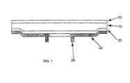
- Each tip is deposited on the thin conductive layer, with or without anchoring in the substrate.
- the substrate can be equipped with a material shock absorber arranged under the thin conductive layer opposite the tip corresponding.
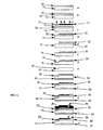
- Step a We start from a monolithic substrate 10 of oxidized silicon by forming an insulating layer 20.
- the substrate is compatible with the UV photolithography technique making it possible to obtain the required precision, in particular less than one micron.
- Other materials can of course be used to make the substrate 10, in particular Arsenium Galium As Ga, quartz, glass.
- Step b A photosensitive resin 12 is coated on the substrate 10, so as to obtain a uniform layer.
- Step c A first UV photolithography operation is then carried out, consisting in producing a local exposure of the resin 12 of the upper layer through a mask 14 having a hole 16 of a predetermined shape. UV radiation is generated by means of an ultraviolet lamp placed above the mask 14.
- Step d the insolated resin 12 is dissolved using a solvent.
- Step e the silicon oxide of the layer 20 is dissolved at the locations released by the resin 12.
- Step f The resin 12 is dissolved using a solvent.
- Step g An anisotropic wet etching of the silicon 10 is then carried out after immersion of the substrate in KOH potash. This results in a non-emerging etching 18 of the substrate which can reach a depth of around 200 microns, and which subsequently constitutes a socket for an electrical contact.
- Step h The silicon oxide 20 remaining on the substrate 10 is eliminated in a solvent bath. There remains the substrate 10 with its etching 18.
- Step i A thermal oxidation of the silicon substrate 10 is carried out, so as to obtain two insulating layers 20 of silicon oxide SiO2 on the two faces of the substrate 10.
- Step j A thin metallic layer 22, for example nickel, gold or aluminum, is then deposited over the entire surface of the upper insulating layer 20. This metal layer 22 is deposited by evaporation under vacuum, or by sputtering.
- Step k This step includes a second UV photolithography operation according to the principle set out in steps b and c, and an etching of the metal layer 22 depending on the location and the shape of the tips to be produced.
- Step I A third UV photolithography operation is then carried out after having deposited on the etched metal layer 22, a thick layer 24 of photosensitive resin, which is revealed with the design of the tips.
- the photolithography operation is followed by an electroforming operation consisting in manufacturing the tips 26 in the form of metal studs 30 microns in diameter, and 60 to 100 microns thick.
- the material of the electroformed pads here is identical to that of the etched metal layer 22.
- Step m The resin layer 24 is finally dissolved in a solvent bath, and the final shape of the implantation of the tip 26 on the monolithic substrate 10 is obtained.
- the multi-point card 28 has a density high peaks 26 thanks to photolithography technology, the pitch between the various tips 26 electrodeposited can be a few tens microns.
- the tips 26 can have different shapes cylindrical with any base, in particular a straight section cylinder constant (figure 4), two superimposed cylinders (figure 5) having possibly different materials, a superposition of cylinders to decreasing diameters in the direction of the height (figure 6), and a shape coaxial (Figure 7) for a frequency test.
- Other sections square, polygonal are also possible.
- FIGS. 8 to 10 The various means of electrical and mechanical connection of the tips 26 on the substrate 10 are illustrated in FIGS. 8 to 10.
- the tip 26 is deposited directly on the thin layer of the conductor 22, extending in a direction perpendicular to the substrate 10.
- the base of the tip 26 is anchored in the substrate 10 in crossing the conductor 22.
- a damping material 30 is arranged in the substrate 10 and under the conductor 22.
- the base of the tip 26 is fixed on the opposite face outside of the conductor 22 as in FIG. 8.
Landscapes
- Physics & Mathematics (AREA)
- General Physics & Mathematics (AREA)
- Testing Or Measuring Of Semiconductors Or The Like (AREA)
- Measuring Leads Or Probes (AREA)
Claims (9)
- Verfahren zur Herstellung einer Karte mit mehreren Spitzen, die insbesondere zum Testen eines oder mehrerer Halbleiterchips oder integrierter Schaltungen vor ihrer Einkapselung bestimmt ist und ein Substrat (10) umfasst, wobei eine der Seiten mit führenden Spuren versehen ist, die mit Kontakten in Form von Spitzen (26) verbunden sind, welches Verfahren durch folgende Schritte gekennzeichnet ist:eine dünne Metallschicht (22) wird durch Aufdampfen im Vakuum oder Kathodenzerstäubung auf eine einzelne Seite des monolithischen Substrats (10) aufgebracht, wobei vor dem Aufbringen der dünnen Metallschicht (22) ein anisotropes Ätzen des Silizium-Substrats (10) erfolgt, welche Ätzung nicht durch das Substrat durchgeht, um eine elektrische Kontaktstelle zu bilden,die leitenden Spuren werden mittels eines UV-Fotolithografie-Arbeitsschritts unter Verwendung eines lichtempfindlichen Harzes hergestellt, woraufhin das Ätzen der dünnen Metallschicht (22) entsprechend den Stellen und der Form der Spitzen (26) erfolgt,anschließend wird ein weiterer UV-Fotolithografie-Arbeitsschritt durchgeführt, der in dem Aufbringen einer dicken Schicht (24) aus lichtempfindlichem Harz auf die geätzte dünne Schicht besteht, wobei in das Harz anschließend das Muster (25) der Spitzen eingeprägt wird,die Spitzen (26) werden durch Galvanoformung mittels eines Metallionenbades hergestellt, wodurch galvanogeformte Höcker entstehen, die der Form der Muster (25) entsprechen,und die verbleibende Harzschicht (24) wird anschließend in einem Lösungsmittelbad aufgelöst, damit die Spitzen (26) endgültig in dem monolithischen Substrat (10) eingearbeitet sind.
- Verfahren zur Herstellung einer Karte mit mehreren Spitzen nach Anspruch 1, dadurch gekennzeichnet, dass das Substrat (10) aus einem Ausgangsmaterial besteht, das unter anderen Silizium, Galliumarsenid, Glas oder Quarz sein kann.
- Verfahren zur Herstellung einer Karte mit mehreren Spitzen nach Anspruch 1 oder 2, dadurch gekennzeichnet, dass die anisotrope Ätzung des Substrats (10) nach einem ersten UV-Fotolithographie-Schritt erfolgt, der darin besteht, durch eine Maske (14) hindurch örtlich begrenzt eine Isolierung einer lichtempfindlichen Harzschicht (12) herzustellen, die vorab auf eine der Seiten des Substrats (10) aufgebracht wurde, und dass die anisotrope Ätzung durch Eintauchen des Siliziumsubstrats (10) in Kaliumhydroxid KOH erhalten wird.
- Verfahren zur Herstellung einer Karte mit mehreren Spitzen nach Anspruch 1, dadurch gekennzeichnet, dass die dünne Metallschicht (22) aus einem Material auf Basis von entweder Nickel, Gold oder Aluminium hergestellt wird.
- Verfahren zur Herstellung einer Karte mit mehreren Spitzen nach Anspruch 4, dadurch gekennzeichnet, dass die Galvanoformung der Spitzen (26) in einem Nickelsulfamatbad erfolgt, und zwar mit einer Stromdichte von 1A/dm2.
- Karte mit mehreren Spitzen zum Testen von Halbleiterchips, die ein Substrat (10) umfasst, das nach dem Verfahren eines der Ansprüche 1 bis 5 behandelt wurde, zum Erreichen einer hohen Dichte von Spitzen (26), wobei der Abstand zwischen den einzelnen Spitzen maximal 100 Mikron beträgt.
- Karte mit mehreren Spitzen nach Anspruch 6, dadurch gekennzeichnet, dass die Höcker der Spitzen (26) einen kreisförmigen oder polygonalen Querschnitt aufweisen.
- Karte mit mehreren Spitzen nach Anspruch 6 oder 7, dadurch gekennzeichnet, dass jede Spitze (26) auf die dünne, leitende Schicht (22) mit oder ohne Verankerung im Substrat (10) aufgebracht wird.
- Karte mit mehreren Spitzen nach Anspruch 6 oder 7, dadurch gekennzeichnet, dass das Substrat (10) mit einem dämpfenden Material (30) versehen ist, das unter der dünnen, leitenden Schicht (22) gegenüber der jeweiligen Spitze (26) vorgesehen ist.
Applications Claiming Priority (3)
| Application Number | Priority Date | Filing Date | Title |
|---|---|---|---|
| FR9704635 | 1997-04-10 | ||
| FR9704635A FR2762140B1 (fr) | 1997-04-10 | 1997-04-10 | Procede de fabrication d'une carte a pointes de contact multiple pour le test des puces semiconductrices |
| PCT/FR1998/000718 WO1998045716A1 (fr) | 1997-04-10 | 1998-04-09 | Procede de fabrication d'une carte a pointes de contact multiple pour le test des puces semiconductrices |
Publications (2)
| Publication Number | Publication Date |
|---|---|
| EP0975979A1 EP0975979A1 (de) | 2000-02-02 |
| EP0975979B1 true EP0975979B1 (de) | 2001-08-22 |
Family
ID=9505938
Family Applications (1)
| Application Number | Title | Priority Date | Filing Date |
|---|---|---|---|
| EP98920596A Expired - Lifetime EP0975979B1 (de) | 1997-04-10 | 1998-04-09 | Verfahren zur herstellung von karten mit mehreren kontaktspitzen zum testen von halbleiterchips |
Country Status (8)
| Country | Link |
|---|---|
| US (1) | US6289583B1 (de) |
| EP (1) | EP0975979B1 (de) |
| JP (1) | JP2001521620A (de) |
| CN (1) | CN1174251C (de) |
| AT (1) | ATE204650T1 (de) |
| DE (1) | DE69801429T2 (de) |
| FR (1) | FR2762140B1 (de) |
| WO (1) | WO1998045716A1 (de) |
Families Citing this family (25)
| Publication number | Priority date | Publication date | Assignee | Title |
|---|---|---|---|---|
| US7063541B2 (en) | 1997-03-17 | 2006-06-20 | Formfactor, Inc. | Composite microelectronic spring structure and method for making same |
| US6420884B1 (en) * | 1999-01-29 | 2002-07-16 | Advantest Corp. | Contact structure formed by photolithography process |
| US6255727B1 (en) * | 1999-08-03 | 2001-07-03 | Advantest Corp. | Contact structure formed by microfabrication process |
| US6579804B1 (en) * | 1998-11-30 | 2003-06-17 | Advantest, Corp. | Contact structure and production method thereof and probe contact assembly using same |
| US6780001B2 (en) * | 1999-07-30 | 2004-08-24 | Formfactor, Inc. | Forming tool for forming a contoured microelectronic spring mold |
| US7189077B1 (en) | 1999-07-30 | 2007-03-13 | Formfactor, Inc. | Lithographic type microelectronic spring structures with improved contours |
| US6939474B2 (en) * | 1999-07-30 | 2005-09-06 | Formfactor, Inc. | Method for forming microelectronic spring structures on a substrate |
| US7435108B1 (en) | 1999-07-30 | 2008-10-14 | Formfactor, Inc. | Variable width resilient conductive contact structures |
| US6888362B2 (en) * | 2000-11-09 | 2005-05-03 | Formfactor, Inc. | Test head assembly for electronic components with plurality of contoured microelectronic spring contacts |
| US6713374B2 (en) | 1999-07-30 | 2004-03-30 | Formfactor, Inc. | Interconnect assemblies and methods |
| US6468098B1 (en) * | 1999-08-17 | 2002-10-22 | Formfactor, Inc. | Electrical contactor especially wafer level contactor using fluid pressure |
| FR2802000B1 (fr) * | 1999-12-01 | 2002-03-22 | Gemplus Card Int | Procede de realisation d'un circuit oscillant accorde et fabrication de dispositifs de radiocommunications de faibles dimensions comprenant un tel circuit |
| FR2812400B1 (fr) * | 2000-07-28 | 2002-09-27 | Mesatronic | Procede de fabrication d'une carte a pointes de contact multiple pour le test de circuits integres a microbilles, et dispositif de test utilisant la carte |
| US7396236B2 (en) | 2001-03-16 | 2008-07-08 | Formfactor, Inc. | Wafer level interposer |
| US6729019B2 (en) | 2001-07-11 | 2004-05-04 | Formfactor, Inc. | Method of manufacturing a probe card |
| WO2003007003A1 (en) * | 2001-07-11 | 2003-01-23 | Formfactor, Inc. | Method of manufacturing a probe card |
| JP4635395B2 (ja) * | 2001-08-28 | 2011-02-23 | 凸版印刷株式会社 | 半導体回路検査治具の製造方法 |
| JP2003078310A (ja) * | 2001-09-04 | 2003-03-14 | Murata Mfg Co Ltd | 高周波用線路変換器、部品、モジュールおよび通信装置 |
| US7122760B2 (en) * | 2002-11-25 | 2006-10-17 | Formfactor, Inc. | Using electric discharge machining to manufacture probes |
| US6945827B2 (en) * | 2002-12-23 | 2005-09-20 | Formfactor, Inc. | Microelectronic contact structure |
| JP2004356362A (ja) * | 2003-05-29 | 2004-12-16 | Dainippon Screen Mfg Co Ltd | プローブカード製造用基板、検査装置、3次元造形装置および3次元造形方法 |
| JP4107275B2 (ja) * | 2004-09-09 | 2008-06-25 | セイコーエプソン株式会社 | 検査用プローブ及び検査装置、検査用プローブの製造方法 |
| CN100348983C (zh) * | 2005-02-07 | 2007-11-14 | 董玟昌 | 一种微机电探针电路薄膜及其制法 |
| EP2360489B1 (de) | 2010-02-04 | 2013-04-17 | Nxp B.V. | Magnetfeldsensor |
| KR101101062B1 (ko) | 2010-08-19 | 2011-12-30 | 삼성에스디아이 주식회사 | 충방전 장치 |
Family Cites Families (13)
| Publication number | Priority date | Publication date | Assignee | Title |
|---|---|---|---|---|
| US5103557A (en) * | 1988-05-16 | 1992-04-14 | Leedy Glenn J | Making and testing an integrated circuit using high density probe points |
| US5323035A (en) * | 1992-10-13 | 1994-06-21 | Glenn Leedy | Interconnection structure for integrated circuits and method for making same |
| US4924589A (en) * | 1988-05-16 | 1990-05-15 | Leedy Glenn J | Method of making and testing an integrated circuit |
| JPH0817192B2 (ja) * | 1988-05-30 | 1996-02-21 | 株式会社日立製作所 | 半導体lsi検査装置用プローブヘッドの製造方法 |
| US5189363A (en) | 1990-09-14 | 1993-02-23 | Ibm Corporation | Integrated circuit testing system having a cantilevered contact lead probe pattern mounted on a flexible tape for interconnecting an integrated circuit to a tester |
| US5177438A (en) * | 1991-08-02 | 1993-01-05 | Motorola, Inc. | Low resistance probe for semiconductor |
| US5177439A (en) * | 1991-08-30 | 1993-01-05 | U.S. Philips Corporation | Probe card for testing unencapsulated semiconductor devices |
| JP2615381B2 (ja) | 1992-10-12 | 1997-05-28 | 株式会社神戸製鋼所 | プローブユニットの製造方法 |
| US5419807A (en) * | 1993-09-03 | 1995-05-30 | Micron Technology, Inc. | Method of providing electrical interconnect between two layers within a silicon substrate, semiconductor apparatus, and method of forming apparatus for testing semiconductor circuitry for operability |
| US5483741A (en) * | 1993-09-03 | 1996-01-16 | Micron Technology, Inc. | Method for fabricating a self limiting silicon based interconnect for testing bare semiconductor dice |
| JP2710544B2 (ja) | 1993-09-30 | 1998-02-10 | インターナショナル・ビジネス・マシーンズ・コーポレイション | プローブ構造、プローブ構造の形成方法 |
| US5475318A (en) * | 1993-10-29 | 1995-12-12 | Robert B. Marcus | Microprobe |
| US5621333A (en) * | 1995-05-19 | 1997-04-15 | Microconnect, Inc. | Contact device for making connection to an electronic circuit device |
-
1997
- 1997-04-10 FR FR9704635A patent/FR2762140B1/fr not_active Expired - Fee Related
-
1998
- 1998-04-09 CN CNB988038986A patent/CN1174251C/zh not_active Expired - Fee Related
- 1998-04-09 WO PCT/FR1998/000718 patent/WO1998045716A1/fr not_active Ceased
- 1998-04-09 JP JP54246698A patent/JP2001521620A/ja active Pending
- 1998-04-09 DE DE69801429T patent/DE69801429T2/de not_active Expired - Fee Related
- 1998-04-09 US US09/381,437 patent/US6289583B1/en not_active Expired - Fee Related
- 1998-04-09 EP EP98920596A patent/EP0975979B1/de not_active Expired - Lifetime
- 1998-04-09 AT AT98920596T patent/ATE204650T1/de not_active IP Right Cessation
Also Published As
| Publication number | Publication date |
|---|---|
| CN1174251C (zh) | 2004-11-03 |
| DE69801429T2 (de) | 2002-05-16 |
| WO1998045716A1 (fr) | 1998-10-15 |
| DE69801429D1 (de) | 2001-09-27 |
| EP0975979A1 (de) | 2000-02-02 |
| JP2001521620A (ja) | 2001-11-06 |
| CN1252129A (zh) | 2000-05-03 |
| FR2762140A1 (fr) | 1998-10-16 |
| FR2762140B1 (fr) | 2000-01-14 |
| ATE204650T1 (de) | 2001-09-15 |
| US6289583B1 (en) | 2001-09-18 |
Similar Documents
| Publication | Publication Date | Title |
|---|---|---|
| EP0975979B1 (de) | Verfahren zur herstellung von karten mit mehreren kontaktspitzen zum testen von halbleiterchips | |
| EP0688033B1 (de) | Magnetischer Mikroschalter und sein Herstellungsverfahren | |
| EP2053646B1 (de) | Verfahren zur vertikalen Verbindung durch Vias in dreidimensionallen elektronischen Modulen | |
| EP0596456A1 (de) | Methode zur Herstellung eines integrierten kapazitiven Transduktors | |
| EP1210733A1 (de) | Herstellung von durchkontakten durch ein substrat | |
| EP0254640A1 (de) | Realisierungsverfahren einer elektronischen Speicher-Karte und durch dieses Verfahren erhaltene Karte | |
| FR2992467A1 (fr) | Procede de realisation d'un composant a contact electrique traversant et composant obtenu | |
| EP2610907A1 (de) | Elektronische Stapelvorrichtung, und Herstellungsverfahren einer solchen elektronischen Vorrichtung | |
| EP2230206A1 (de) | Form für Galvanoplastik und ihr Herstellungsverfahren | |
| FR2596921A1 (fr) | Procede de formation d'un dessin conducteur sur la surface d'un semi-conducteur tel que notamment du silicium, germanium et l'arsenium de gallium | |
| EP3742478B1 (de) | Selbstassemblierungsverfahren mit hybrider molekülverbindung | |
| EP2772943A1 (de) | Herstellungsverfahren einer mikroelektronischen Vorrichtung und entsprechende Vorrichtung | |
| EP1890958B1 (de) | Mikromechanische komponente mit aktiven elementen und verfahren zur herstellung einer komponente dieser art | |
| EP0446112A1 (de) | Elastomer-Verbindung für integrierte Schaltungen oder ähnliche Anordnungen und Herstellungsverfahren dafür | |
| EP1719173A1 (de) | Mikroelektronische verbindungseinrichtung mit lokalisierten leitfähigen pins | |
| EP0864094B1 (de) | Struktur mit einem isolierten teil in einem massiven substrat und verfahren zu deren erzeugung | |
| EP0188946B1 (de) | Integriertes Kapazitätselement auf einer Scheibe einer integrierten Schaltung und Verfahren zum Herstellen dieses Kapazitätselementes | |
| WO2005015596A2 (fr) | Procede de croissance localisee de nanofils ou nanotubes | |
| KR100503983B1 (ko) | 반도체 칩 테스트용의 다수의 접촉팁들을 구비하는 카드의 제조방법 | |
| FR2779243A1 (fr) | Procede de realisation par photolithographie d'ouvertures auto-alignees sur une structure, en particulier pour ecran plat a micropointes | |
| FR3089016A1 (fr) | Procede de test electrique d’au moins un dispositif electronique destine a etre colle par collage direct | |
| EP1697783A1 (de) | Optische komponenten und herstellung dafür | |
| JPH11310497A (ja) | 導体又は半導体材料からなる単結晶層を製造する方法 | |
| EP4639628A1 (de) | Verfahren zur herstellung einer platte mit zwei zonen mit einem benetzbarkeitskontrast über 90 ° und so hergestellte platte | |
| FR2749974A1 (fr) | Procede de montage d'un circuit integre sur un support et support en resultant |
Legal Events
| Date | Code | Title | Description |
|---|---|---|---|
| PUAI | Public reference made under article 153(3) epc to a published international application that has entered the european phase |
Free format text: ORIGINAL CODE: 0009012 |
|
| 17P | Request for examination filed |
Effective date: 19991021 |
|
| AK | Designated contracting states |
Kind code of ref document: A1 Designated state(s): AT BE CH DE ES FI FR GB IE IT LI NL PT SE |
|
| GRAG | Despatch of communication of intention to grant |
Free format text: ORIGINAL CODE: EPIDOS AGRA |
|
| GRAG | Despatch of communication of intention to grant |
Free format text: ORIGINAL CODE: EPIDOS AGRA |
|
| GRAG | Despatch of communication of intention to grant |
Free format text: ORIGINAL CODE: EPIDOS AGRA |
|
| GRAH | Despatch of communication of intention to grant a patent |
Free format text: ORIGINAL CODE: EPIDOS IGRA |
|
| 17Q | First examination report despatched |
Effective date: 20010126 |
|
| GRAH | Despatch of communication of intention to grant a patent |
Free format text: ORIGINAL CODE: EPIDOS IGRA |
|
| GRAA | (expected) grant |
Free format text: ORIGINAL CODE: 0009210 |
|
| AK | Designated contracting states |
Kind code of ref document: B1 Designated state(s): AT BE CH DE ES FI FR GB IE IT LI NL PT SE |
|
| PG25 | Lapsed in a contracting state [announced via postgrant information from national office to epo] |
Ref country code: IE Free format text: LAPSE BECAUSE OF FAILURE TO SUBMIT A TRANSLATION OF THE DESCRIPTION OR TO PAY THE FEE WITHIN THE PRESCRIBED TIME-LIMIT Effective date: 20010822 Ref country code: FI Free format text: LAPSE BECAUSE OF FAILURE TO SUBMIT A TRANSLATION OF THE DESCRIPTION OR TO PAY THE FEE WITHIN THE PRESCRIBED TIME-LIMIT Effective date: 20010822 Ref country code: AT Free format text: LAPSE BECAUSE OF FAILURE TO SUBMIT A TRANSLATION OF THE DESCRIPTION OR TO PAY THE FEE WITHIN THE PRESCRIBED TIME-LIMIT Effective date: 20010822 |
|
| REF | Corresponds to: |
Ref document number: 204650 Country of ref document: AT Date of ref document: 20010915 Kind code of ref document: T |
|
| REG | Reference to a national code |
Ref country code: CH Ref legal event code: EP |
|
| REF | Corresponds to: |
Ref document number: 69801429 Country of ref document: DE Date of ref document: 20010927 |
|
| REG | Reference to a national code |
Ref country code: IE Ref legal event code: FG4D Free format text: FRENCH |
|
| PG25 | Lapsed in a contracting state [announced via postgrant information from national office to epo] |
Ref country code: SE Free format text: LAPSE BECAUSE OF FAILURE TO SUBMIT A TRANSLATION OF THE DESCRIPTION OR TO PAY THE FEE WITHIN THE PRESCRIBED TIME-LIMIT Effective date: 20011122 Ref country code: PT Free format text: LAPSE BECAUSE OF FAILURE TO SUBMIT A TRANSLATION OF THE DESCRIPTION OR TO PAY THE FEE WITHIN THE PRESCRIBED TIME-LIMIT Effective date: 20011122 |
|
| GBT | Gb: translation of ep patent filed (gb section 77(6)(a)/1977) |
Effective date: 20011117 |
|
| REG | Reference to a national code |
Ref country code: GB Ref legal event code: IF02 |
|
| PG25 | Lapsed in a contracting state [announced via postgrant information from national office to epo] |
Ref country code: ES Free format text: LAPSE BECAUSE OF FAILURE TO SUBMIT A TRANSLATION OF THE DESCRIPTION OR TO PAY THE FEE WITHIN THE PRESCRIBED TIME-LIMIT Effective date: 20020228 |
|
| PG25 | Lapsed in a contracting state [announced via postgrant information from national office to epo] |
Ref country code: LI Free format text: LAPSE BECAUSE OF NON-PAYMENT OF DUE FEES Effective date: 20020430 Ref country code: CH Free format text: LAPSE BECAUSE OF NON-PAYMENT OF DUE FEES Effective date: 20020430 Ref country code: BE Free format text: LAPSE BECAUSE OF NON-PAYMENT OF DUE FEES Effective date: 20020430 |
|
| REG | Reference to a national code |
Ref country code: IE Ref legal event code: FD4D |
|
| PLBE | No opposition filed within time limit |
Free format text: ORIGINAL CODE: 0009261 |
|
| STAA | Information on the status of an ep patent application or granted ep patent |
Free format text: STATUS: NO OPPOSITION FILED WITHIN TIME LIMIT |
|
| 26N | No opposition filed | ||
| REG | Reference to a national code |
Ref country code: CH Ref legal event code: PL |
|
| PG25 | Lapsed in a contracting state [announced via postgrant information from national office to epo] |
Ref country code: FR Free format text: LAPSE BECAUSE OF NON-PAYMENT OF DUE FEES Effective date: 20021231 |
|
| REG | Reference to a national code |
Ref country code: FR Ref legal event code: ST |
|
| PGFP | Annual fee paid to national office [announced via postgrant information from national office to epo] |
Ref country code: NL Payment date: 20070403 Year of fee payment: 10 |
|
| PGFP | Annual fee paid to national office [announced via postgrant information from national office to epo] |
Ref country code: DE Payment date: 20070405 Year of fee payment: 10 |
|
| PGFP | Annual fee paid to national office [announced via postgrant information from national office to epo] |
Ref country code: GB Payment date: 20070404 Year of fee payment: 10 |
|
| PGFP | Annual fee paid to national office [announced via postgrant information from national office to epo] |
Ref country code: IT Payment date: 20070523 Year of fee payment: 10 |
|
| GBPC | Gb: european patent ceased through non-payment of renewal fee |
Effective date: 20080409 |
|
| NLV4 | Nl: lapsed or anulled due to non-payment of the annual fee |
Effective date: 20081101 |
|
| PG25 | Lapsed in a contracting state [announced via postgrant information from national office to epo] |
Ref country code: NL Free format text: LAPSE BECAUSE OF NON-PAYMENT OF DUE FEES Effective date: 20081101 Ref country code: DE Free format text: LAPSE BECAUSE OF NON-PAYMENT OF DUE FEES Effective date: 20081101 |
|
| PG25 | Lapsed in a contracting state [announced via postgrant information from national office to epo] |
Ref country code: GB Free format text: LAPSE BECAUSE OF NON-PAYMENT OF DUE FEES Effective date: 20080409 |
|
| PG25 | Lapsed in a contracting state [announced via postgrant information from national office to epo] |
Ref country code: IT Free format text: LAPSE BECAUSE OF NON-PAYMENT OF DUE FEES Effective date: 20080409 |