EP0975979B1 - Method for making cards with multiple contact tips for testing semiconductor chips - Google Patents
Method for making cards with multiple contact tips for testing semiconductor chips Download PDFInfo
- Publication number
- EP0975979B1 EP0975979B1 EP98920596A EP98920596A EP0975979B1 EP 0975979 B1 EP0975979 B1 EP 0975979B1 EP 98920596 A EP98920596 A EP 98920596A EP 98920596 A EP98920596 A EP 98920596A EP 0975979 B1 EP0975979 B1 EP 0975979B1
- Authority
- EP
- European Patent Office
- Prior art keywords
- tips
- substrate
- layer
- card
- tip
- Prior art date
- Legal status (The legal status is an assumption and is not a legal conclusion. Google has not performed a legal analysis and makes no representation as to the accuracy of the status listed.)
- Expired - Lifetime
Links
Images


Classifications
-
- G—PHYSICS
- G01—MEASURING; TESTING
- G01R—MEASURING ELECTRIC VARIABLES; MEASURING MAGNETIC VARIABLES
- G01R1/00—Details of instruments or arrangements of the types included in groups G01R5/00 - G01R13/00 and G01R31/00
- G01R1/02—General constructional details
- G01R1/06—Measuring leads; Measuring probes
- G01R1/067—Measuring probes
- G01R1/073—Multiple probes
- G01R1/07307—Multiple probes with individual probe elements, e.g. needles, cantilever beams or bump contacts, fixed in relation to each other, e.g. bed of nails fixture or probe card
- G01R1/07342—Multiple probes with individual probe elements, e.g. needles, cantilever beams or bump contacts, fixed in relation to each other, e.g. bed of nails fixture or probe card the body of the probe being at an angle other than perpendicular to test object, e.g. probe card
-
- G—PHYSICS
- G01—MEASURING; TESTING
- G01R—MEASURING ELECTRIC VARIABLES; MEASURING MAGNETIC VARIABLES
- G01R3/00—Apparatus or processes specially adapted for the manufacture or maintenance of measuring instruments, e.g. of probe tips
-
- G—PHYSICS
- G01—MEASURING; TESTING
- G01R—MEASURING ELECTRIC VARIABLES; MEASURING MAGNETIC VARIABLES
- G01R1/00—Details of instruments or arrangements of the types included in groups G01R5/00 - G01R13/00 and G01R31/00
- G01R1/02—General constructional details
- G01R1/06—Measuring leads; Measuring probes
- G01R1/067—Measuring probes
- G01R1/06711—Probe needles; Cantilever beams; "Bump" contacts; Replaceable probe pins
- G01R1/06733—Geometry aspects
-
- Y—GENERAL TAGGING OF NEW TECHNOLOGICAL DEVELOPMENTS; GENERAL TAGGING OF CROSS-SECTIONAL TECHNOLOGIES SPANNING OVER SEVERAL SECTIONS OF THE IPC; TECHNICAL SUBJECTS COVERED BY FORMER USPC CROSS-REFERENCE ART COLLECTIONS [XRACs] AND DIGESTS
- Y10—TECHNICAL SUBJECTS COVERED BY FORMER USPC
- Y10T—TECHNICAL SUBJECTS COVERED BY FORMER US CLASSIFICATION
- Y10T29/00—Metal working
- Y10T29/49—Method of mechanical manufacture
- Y10T29/49002—Electrical device making
- Y10T29/49117—Conductor or circuit manufacturing
Landscapes
- Physics & Mathematics (AREA)
- General Physics & Mathematics (AREA)
- Testing Or Measuring Of Semiconductors Or The Like (AREA)
- Measuring Leads Or Probes (AREA)
Abstract
Description
L'invention est relative à un procédé de fabrication d'une carte à pointes multiple, destinée notamment à tester les puces semiconductrices ou des circuits intégrés avant leur encapsulation, et comprenant un substrat dont l'une des faces est dotée de pistes conductrices connectées à des contacts en forme de pointes.The invention relates to a method for manufacturing a spike card multiple, intended in particular to test semiconductor chips or integrated circuits before their encapsulation, and comprising a substrate of which one of the faces is provided with conductive tracks connected to contacts in shape of spikes.
Les cartes à pointes sont utilisées pour le contrôle des puces ou circuits intégrés après fabrication, et avant leur encapsulation. Les cartes connues à ce jour utilisent généralement différents types de technologies, à savoir les cartes à pointes à lames soudées, les cartes à anneaux époxy, et les cartes à membranes, telles que décrites dans les documents EP-A-0475050, WO9409374, et EP-0646800. La mise en place des pointes sur ces cartes connues est néanmoins limitée à un nombre donné de pointes, lequel n'est plus adapté à l'évolution de l'intégration des puces semiconductrices.Spike cards are used to control chips or circuits integrated after manufacture, and before their encapsulation. The cards known to today generally use different types of technology, namely soldered tip cards, epoxy ring cards, and membranes, as described in documents EP-A-0475050, WO9409374, and EP-0646800. The placement of spikes on these cards known is however limited to a given number of tips, which is not more suited to the evolution of the integration of semiconductor chips.
Le document WO 96/36884 décrit un procédé de fabrication d'une carte faisant l'objet d'une découpe préalable pour obtenir un système de lamelles flexibles. Les pistes de connexion ne sont pas monocouches, et ne fait pas usage d'une gravure anisotrope d'un substrat monolithique.WO 96/36884 describes a method of manufacturing a card pre-cut to obtain a slat system flexible. Connection tracks are not monolayers, and do not use of an anisotropic etching of a monolithic substrate.
Un premier objet de l'invention consiste à élaborer un procédé de fabrication d'une carte à pointes multiple permettant d'augmenter la précision et la densité d'implantation des contacts.A first object of the invention consists in developing a manufacturing process a multi-point card to increase the precision and density of contacts.
Le procédé de fabrication est caractérisé par les étapes suivantes :
- une couche mince métallique est déposée par évaporation sous vide ou par pulvérisation cathodique sur l'une des faces isolée du substrat monolithique, une gravure anisotrope du substrat de silicium étant réalisée avant l'obtention des pistes conductrices, ladite gravure étant non débouchante pour constituer une prise de contact électrique
- les pistes conductrices sont obtenues par gravure directe,
- on réalise par la suite une opération de photolithographie UV consistant à déposer une couche épaisse de résine photosensible sur la couche mince gravée, la résine étant ensuite révélée avec le dessin des pointes,
- on fabrique les pointes par électroformage au moyen d'un bain d'ions métalliques permettant d'obtenir des plots électroformés correspondant à la forme des dessins,
- et la couche restante de résine est finalement dissoute dans un bain de solvant pour obtenir l'implantation définitive des pointes sur le substrat monolithique.
- a thin metallic layer is deposited by vacuum evaporation or by sputtering on one of the insulated faces of the monolithic substrate, an anisotropic etching of the silicon substrate being carried out before the conductive tracks are obtained, said etching being non-emerging to constitute a electrical contact
- the conductive tracks are obtained by direct etching,
- a UV photolithography operation is subsequently carried out consisting of depositing a thick layer of photosensitive resin on the etched thin layer, the resin then being revealed with the design of the tips,
- the tips are manufactured by electroforming by means of a metal ion bath making it possible to obtain electroformed pads corresponding to the shape of the drawings,
- and the remaining layer of resin is finally dissolved in a solvent bath to obtain the final implantation of the tips on the monolithic substrate.
La gravure anisotrope est obtenue avantageusement par immersion du substrat de silicium dans de la potasse KOH.Anisotropic etching is advantageously obtained by immersion of the silicon substrate in KOH potash.
Selon une caractéristique du procédé, la gravure anisotrope du substrat intervient après une première photolithographie UV consistant à produire à travers un masque une insolation locale d'une couche de résine photosensible enduite préalablement sur une des faces du substrat.According to a characteristic of the process, the anisotropic etching of the substrate comes after a first UV photolithography consisting in producing through a mask local exposure to a layer of resin photosensitive previously coated on one side of the substrate.
La couche mince métallique peut être formée à titre d'exemple par un matériau à base de nickel, d'or, ou d'aluminium. Tout autre matériau métallique conducteur peut bien entendu être utilisé.The metallic thin layer can be formed, for example, by a material based on nickel, gold, or aluminum. Any other material conductive metal can of course be used.
Un deuxième objet de l'invention consiste également à réaliser une carte à pointes multiple, dans laquelle le pas entre les différentes pointes est réduit au minimum, de manière à obtenir une haute densité de contacts.A second object of the invention also consists in making a card for multiple points, in which the pitch between the different points is reduced to minimum, so as to obtain a high density of contacts.
Les pointes obtenues par une photolithographie UV épaisse et un électroformage, sont formées par des plots métalliques de 10 à 100 microns de diamètre, et de 10 à quelques dizaines de microns d'épaisseur. Les sections des plots peuvent également être de sections carrées ou polygonales. The tips obtained by thick UV photolithography and a electroforming, are formed by metal pads from 10 to 100 microns in diameter, and from 10 to a few tens of microns thick. The sections of the studs can also be square sections or polygonal.
Chaque pointe est déposée sur la couche mince conductrice, avec ou sans ancrage dans le substrat. Le substrat peut être équipé d'un matériau amortisseur agencé sous la couche mince conductrice à l'opposé de la pointe correspondante.Each tip is deposited on the thin conductive layer, with or without anchoring in the substrate. The substrate can be equipped with a material shock absorber arranged under the thin conductive layer opposite the tip corresponding.
D'autres avantages et caractéristiques ressortiront plus clairement de la description du procédé de fabrication qui va suivre, ainsi que des différentes formes de réalisation des pointes illustrées aux dessins annexés, dans lesquels
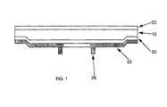
- la figure 1 montre une carte obtenue selon le procédé de l'invention ;
- la figure 2 représente une vue générale en coupe verticale du substrat équipé des pointes électroformées ;
- la figure 3 est une vue en plan de la figure 2 ;
- les figures 4 à 7 montrent différentes formes de pointes en fonction de l'application de la carte ;
- les figures 8 à 10 représentent différents moyens de liaison électrique et mécanique des pointes sur le substrat ;
- la figure 11 montre une variante de la figure 1, avec un substrat à trous métallisés pour ramener la connexion électrique sur la face opposée aux pointes.
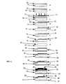
- la figure 12 montre un exemple des différentes étapes a-m chronologiques mises en oeuvre lors du procédé de fabrication selon l'invention;
- Figure 1 shows a map obtained according to the method of the invention;
- FIG. 2 represents a general view in vertical section of the substrate equipped with the electroformed tips;
- Figure 3 is a plan view of Figure 2;
- Figures 4 to 7 show different shapes of tips depending on the application of the card;
- Figures 8 to 10 show different means of electrical and mechanical connection of the tips on the substrate;
- FIG. 11 shows a variant of FIG. 1, with a substrate with metallized holes for bringing the electrical connection back to the face opposite the tips.
- FIG. 12 shows an example of the various chronological stages implemented during the manufacturing process according to the invention;
Les différentes étapes de l'exemple de procédé pour la mise en oeuvre de la carte à pointes multiple pour le contrôle des puces après fabrication, sont illustrées sur le schéma de la figure 12 à titre indicatif.The different stages of the example process for implementing the multiple point card for post-manufacturing chip control, are illustrated in the diagram in FIG. 12 for information.
Etape a : On part d'un substrat 10 monolithique en silicium oxydé en formant
une couche isolante 20. Le substrat est compatible avec la technique de
photolithographie UV permettant d'obtenir des précisions requises,
notamment inférieures au micron. D'autres matériaux peuvent bien entendu
être utilisés pour réaliser le substrat 10, notamment l'Arsenium Galium As Ga,
le quartz, le verre. Step a : We start from a
Etape b : Une résine 12 photosensible est enduite sur le substrat 10, de
manière à obtenir une couche uniforme. Step b : A
Etape c : On réalise ensuite une première opération de photolithographie UV,
consistant à produire une insolation locale de la résine 12 de la couche
supérieure à travers un masque 14 ayant un trou 16 d'une forme
prédéterminée. Le rayonnement UV est engendré au moyen d'une lampe à
ultra-violet disposée au dessus du masque 14.
Etape d : la résine 12 insolée est dissoute au moyen d'un solvant.
Etape e : l'oxyde de silicium de la couche 20 est dissout aux endroits dégagés
par la résine 12.
Etape f : La résine 12 est dissoute au moyen d'un solvant. Step c: A first UV photolithography operation is then carried out, consisting in producing a local exposure of the
Step d: the insolated
Step e: the silicon oxide of the
Step f: The
Etape g : On effectue ensuite une gravure humide anisotrope du silicium 10
après immersion du substrat dans de la potasse KOH. Il en résulte une
gravure 18 non débouchante du substrat pouvant atteindre une profondeur
d'environ 200 microns, et constituant par la suite une prise pour un contact
électrique. Step g: An anisotropic wet etching of the
Etape h : L'oxyde de silicium 20 restant sur le substrat 10 est éliminée dans un
bain de solvant. Il reste le substrat 10 avec sa gravure 18. Step h: The
Etape i : On réalise une oxydation thermique du substrat 10 de silicium, de
manière à obtenir deux couches 20 isolantes d'oxyde de silicium SiO2 sur les
deux faces du substrat 10. Step i: A thermal oxidation of the
Etape j : Une couche mince métallique 22, par exemple du nickel, de l'or ou
de l'aluminium, est ensuite déposée sur toute la surface de la couche isolante
20 supérieure. Le dépôt de cette couche 22 métallique s'effectue par
évaporation sous vide, ou par pulvérisation cathodique . Step j: A thin
Etape k : Cette étape comporte une deuxième opération de photolithographie
UV selon le principe exposé aux étapes b et c, et une gravure de la couche
métallique 22 suivant l'endroit et la forme des pointes à réaliser. Step k: This step includes a second UV photolithography operation according to the principle set out in steps b and c, and an etching of the
Etape I: On réalise ensuite une troisième opération de photolithographie UV
après avoir déposé sur la couche métallique 22 gravée, une épaisse couche
24 de résine photosensible, laquelle est révélée avec le dessin des pointes.
L'opération de photolithographie est suivie par une opération
d'électroformage consistant à fabriquer les pointes 26 sous la forme de plots
métalliques de 30 microns de diamètre, et de 60 à 100 microns d'épaisseur.
Le matériau des plots électroformés est ici identique à celui de la couche
métallique 22 gravée. Step I: A third UV photolithography operation is then carried out after having deposited on the etched
Etape m: La couche 24 de résine est finalement dissoute dans un bain de
solvant, et on obtient la forme définitive de l'implantation de la pointe 26 sur le
substrat 10 monolithique. Step m: The
Sur les figures 2 et 3, la carte 28 à pointes multiple comporte une densité
élevée de pointes 26 grâce à la technologie de photolithographie, le pas entre
les différentes pointes 26 électrodéposées pouvant être de quelques dizaines
de microns.In FIGS. 2 and 3, the
En référence aux figures 4 à 7, les pointes 26 peuvent avoir différentes formes
cylindriques à base quelconque, notamment un cylindre droit à section
constante (figure 4), deux cylindres superposés (figure 5) ayant
éventuellement des matériaux différents, une superposition de cylindres à
diamètres décroissants dans le sens de la hauteur (figure 6), et une forme
coaxiale (figure 7) pour un test en fréquence. D'autres sections (carrées,
polygonales) sont également possibles.With reference to FIGS. 4 to 7, the
Les divers moyens de liaison électrique et mécanique des pointes 26 sur le
substrat 10 sont illustrés sur les figures 8 à 10.The various means of electrical and mechanical connection of the
A la figure 8, la pointe 26 est déposée directement sur la couche mince du
conducteur 22, en s'étendant selon une direction perpendiculaire au substrat
10.In FIG. 8, the
A la figure 9, la base de la pointe 26 est ancrée dans le substrat 10 en
traversant le conducteur 22.In FIG. 9, the base of the
A la figure 10, un matériau amortisseur 30 est agencé dans le substrat 10 et
sous le conducteur 22. La base de la pointe 26 est fixée sur la face opposée
extérieure du conducteur 22 comme dans la figure 8. In FIG. 10, a damping material 30 is arranged in the
Au lieu de déposer des pistes conductrices en couches minces sur un substrat
gravé (comme dans le cas de la figure 1), il est également possible selon la
figure 11 de prévoir des trous métallisés 32 traversant le substrat 10 pour
ramener la connexion électrique sur la face opposée 34 aux pointes 26.Instead of depositing conductive tracks in thin layers on a substrate
engraved (as in the case of figure 1), it is also possible according to the
Figure 11 to provide metallized
Claims (9)
- A process for manufacturing a card with multiple tips designed in particular for testing one or more semiconductor chips or integrated circuits before encapsulation thereof, and comprising a substrate (10), one of the surfaces being provided with conducting strips connected to contacts in the form of tips (26), said process being characterized by the following stagesa thin metal layer (22) is deposited by vapour deposition in a vacuum or by cathode sputtering on one of the insulated surfaces of the monolithic substrate (10), anisotropic etching of the silicon substrate (10) being performed before deposition of the thin metal layer (22) is performed, said etching being non-emergent to constitute an electrical contact connection point,the conducting strips are obtained by means of a UV photolithography operation making use of a photosensitive resin, followed by etching of the thin metal layer (22) according to the location and shape of the tips (26),another UV photolithography operation is then performed consisting in depositing a thick layer (24) of photosensitive resin on the thin etched layer, the resin then being revealed with the drawing (25) of the tips,the tips (26) are manufactured by electroforming by means of a metal ion bath enabling electroformed pads corresponding to the shape of the drawings (25) to be obtained,and the remaining layer (24) of resin is finally dissolved in a solvent bath to obtain the final implantation of the tips (26) on the monolithic substrate (10).
- The process for manufacturing a card with multiple tips according to claim 1. characterized in that the substrate (10) is formed by a material with a base which may among others be silicon, Gallium Arsenide, glass or quartz.
- The process for manufacturing a card with multiple tips according to claim 1 or 2, characterized in that anisotropic etching of the substrate (10) takes place after a first UV photolithography consisting in producing through a mask (14) a local insulation of a layer of photosensitive resin (12) previously deposited on one of the surfaces of the substrate (10). and that anisotropic etching is achieved by immersion of the silicon substrate (10) in potassium hydroxide KOH.
- The process for manufacturing a card with multiple tips according to claim 1, characterized in that the thin metal layer (22) is formed by a nickel-, gold- or aluminium-based material.
- The process for manufacturing a card with multiple tips according to claim 4, characterized in that electroforming of the tips (26) is performed in a nickel sulfamate bath with a current density of about 1A/dm2.
- A multiple-tip card for testing semiconductor chips, and comprising a substrate (10) processed according to the process of one of the claims 1 to 5 to obtain a high density of tips (26), the pitch between the different tips being a maximum of 100 microns.
- The multiple-tip card according to claim 6, characterized in that the pads of the tips (26) have circular or polygonal cross sections.
- The multiple-tip card according to claim 6 or 7, characterized in that each tip (26) is deposited on the thin conducting layer (22), with or without securing in the substrate (10).
- The multiple-tip card according to claim 6 or 7, characterized in that the substrate (10) is equipped with a damping material (30) arranged under the thin conducting layer (22) opposite the corresponding tip (26).
Applications Claiming Priority (3)
| Application Number | Priority Date | Filing Date | Title |
|---|---|---|---|
| FR9704635 | 1997-04-10 | ||
| FR9704635A FR2762140B1 (en) | 1997-04-10 | 1997-04-10 | METHOD FOR MANUFACTURING A MULTIPLE CONTACT POINT CARD FOR TESTING SEMICONDUCTOR CHIPS |
| PCT/FR1998/000718 WO1998045716A1 (en) | 1997-04-10 | 1998-04-09 | Method for making cards with multiple contact tips for testing semiconductor chips |
Publications (2)
| Publication Number | Publication Date |
|---|---|
| EP0975979A1 EP0975979A1 (en) | 2000-02-02 |
| EP0975979B1 true EP0975979B1 (en) | 2001-08-22 |
Family
ID=9505938
Family Applications (1)
| Application Number | Title | Priority Date | Filing Date |
|---|---|---|---|
| EP98920596A Expired - Lifetime EP0975979B1 (en) | 1997-04-10 | 1998-04-09 | Method for making cards with multiple contact tips for testing semiconductor chips |
Country Status (8)
| Country | Link |
|---|---|
| US (1) | US6289583B1 (en) |
| EP (1) | EP0975979B1 (en) |
| JP (1) | JP2001521620A (en) |
| CN (1) | CN1174251C (en) |
| AT (1) | ATE204650T1 (en) |
| DE (1) | DE69801429T2 (en) |
| FR (1) | FR2762140B1 (en) |
| WO (1) | WO1998045716A1 (en) |
Families Citing this family (25)
| Publication number | Priority date | Publication date | Assignee | Title |
|---|---|---|---|---|
| US7063541B2 (en) | 1997-03-17 | 2006-06-20 | Formfactor, Inc. | Composite microelectronic spring structure and method for making same |
| US6579804B1 (en) * | 1998-11-30 | 2003-06-17 | Advantest, Corp. | Contact structure and production method thereof and probe contact assembly using same |
| US6420884B1 (en) * | 1999-01-29 | 2002-07-16 | Advantest Corp. | Contact structure formed by photolithography process |
| US6255727B1 (en) * | 1999-08-03 | 2001-07-03 | Advantest Corp. | Contact structure formed by microfabrication process |
| US6939474B2 (en) * | 1999-07-30 | 2005-09-06 | Formfactor, Inc. | Method for forming microelectronic spring structures on a substrate |
| US7435108B1 (en) * | 1999-07-30 | 2008-10-14 | Formfactor, Inc. | Variable width resilient conductive contact structures |
| US6713374B2 (en) | 1999-07-30 | 2004-03-30 | Formfactor, Inc. | Interconnect assemblies and methods |
| US6780001B2 (en) * | 1999-07-30 | 2004-08-24 | Formfactor, Inc. | Forming tool for forming a contoured microelectronic spring mold |
| US6888362B2 (en) * | 2000-11-09 | 2005-05-03 | Formfactor, Inc. | Test head assembly for electronic components with plurality of contoured microelectronic spring contacts |
| US7189077B1 (en) | 1999-07-30 | 2007-03-13 | Formfactor, Inc. | Lithographic type microelectronic spring structures with improved contours |
| US6468098B1 (en) * | 1999-08-17 | 2002-10-22 | Formfactor, Inc. | Electrical contactor especially wafer level contactor using fluid pressure |
| FR2802000B1 (en) * | 1999-12-01 | 2002-03-22 | Gemplus Card Int | METHOD FOR PRODUCING A TUNED OSCILLATING CIRCUIT AND MANUFACTURING LOW-DIMENSIONAL RADIOCOMMUNICATIONS DEVICES COMPRISING SUCH A CIRCUIT |
| FR2812400B1 (en) | 2000-07-28 | 2002-09-27 | Mesatronic | METHOD FOR MANUFACTURING A MULTIPLE CONTACT POINT CARD FOR TESTING MICROBALL INTEGRATED CIRCUITS, AND TEST DEVICE USING THE CARD |
| US7396236B2 (en) | 2001-03-16 | 2008-07-08 | Formfactor, Inc. | Wafer level interposer |
| CN1288450C (en) * | 2001-07-11 | 2006-12-06 | 佛姆法克特股份有限公司 | Method of manufacturing a probe card |
| US6729019B2 (en) | 2001-07-11 | 2004-05-04 | Formfactor, Inc. | Method of manufacturing a probe card |
| JP4635395B2 (en) * | 2001-08-28 | 2011-02-23 | 凸版印刷株式会社 | Manufacturing method of semiconductor circuit inspection jig |
| JP2003078310A (en) * | 2001-09-04 | 2003-03-14 | Murata Mfg Co Ltd | Line converter for high frequency, component, module, and communication apparatus |
| US7122760B2 (en) * | 2002-11-25 | 2006-10-17 | Formfactor, Inc. | Using electric discharge machining to manufacture probes |
| US6945827B2 (en) * | 2002-12-23 | 2005-09-20 | Formfactor, Inc. | Microelectronic contact structure |
| JP2004356362A (en) * | 2003-05-29 | 2004-12-16 | Dainippon Screen Mfg Co Ltd | Substrate for manufacturing probe card, testing device, device, and method for three-dimensional molding |
| JP4107275B2 (en) | 2004-09-09 | 2008-06-25 | セイコーエプソン株式会社 | Inspection probe and inspection apparatus, and inspection probe manufacturing method |
| CN100348983C (en) * | 2005-02-07 | 2007-11-14 | 董玟昌 | Circuit film for micro electromechanical probe and fabricating method thereof |
| EP2360489B1 (en) * | 2010-02-04 | 2013-04-17 | Nxp B.V. | Magnetic field sensor |
| KR101101062B1 (en) | 2010-08-19 | 2011-12-30 | 삼성에스디아이 주식회사 | Apparatus for charging and discharging |
Family Cites Families (13)
| Publication number | Priority date | Publication date | Assignee | Title |
|---|---|---|---|---|
| US5103557A (en) * | 1988-05-16 | 1992-04-14 | Leedy Glenn J | Making and testing an integrated circuit using high density probe points |
| US4924589A (en) * | 1988-05-16 | 1990-05-15 | Leedy Glenn J | Method of making and testing an integrated circuit |
| US5323035A (en) * | 1992-10-13 | 1994-06-21 | Glenn Leedy | Interconnection structure for integrated circuits and method for making same |
| JPH0817192B2 (en) * | 1988-05-30 | 1996-02-21 | 株式会社日立製作所 | Method for manufacturing probe head for semiconductor LSI inspection device |
| US5189363A (en) | 1990-09-14 | 1993-02-23 | Ibm Corporation | Integrated circuit testing system having a cantilevered contact lead probe pattern mounted on a flexible tape for interconnecting an integrated circuit to a tester |
| US5177438A (en) * | 1991-08-02 | 1993-01-05 | Motorola, Inc. | Low resistance probe for semiconductor |
| US5177439A (en) * | 1991-08-30 | 1993-01-05 | U.S. Philips Corporation | Probe card for testing unencapsulated semiconductor devices |
| JP2615381B2 (en) | 1992-10-12 | 1997-05-28 | 株式会社神戸製鋼所 | Method of manufacturing probe unit |
| US5419807A (en) * | 1993-09-03 | 1995-05-30 | Micron Technology, Inc. | Method of providing electrical interconnect between two layers within a silicon substrate, semiconductor apparatus, and method of forming apparatus for testing semiconductor circuitry for operability |
| US5483741A (en) * | 1993-09-03 | 1996-01-16 | Micron Technology, Inc. | Method for fabricating a self limiting silicon based interconnect for testing bare semiconductor dice |
| JP2710544B2 (en) | 1993-09-30 | 1998-02-10 | インターナショナル・ビジネス・マシーンズ・コーポレイション | Probe structure, method of forming probe structure |
| US5475318A (en) * | 1993-10-29 | 1995-12-12 | Robert B. Marcus | Microprobe |
| US5621333A (en) * | 1995-05-19 | 1997-04-15 | Microconnect, Inc. | Contact device for making connection to an electronic circuit device |
-
1997
- 1997-04-10 FR FR9704635A patent/FR2762140B1/en not_active Expired - Fee Related
-
1998
- 1998-04-09 WO PCT/FR1998/000718 patent/WO1998045716A1/en active IP Right Grant
- 1998-04-09 EP EP98920596A patent/EP0975979B1/en not_active Expired - Lifetime
- 1998-04-09 JP JP54246698A patent/JP2001521620A/en active Pending
- 1998-04-09 DE DE69801429T patent/DE69801429T2/en not_active Expired - Fee Related
- 1998-04-09 AT AT98920596T patent/ATE204650T1/en not_active IP Right Cessation
- 1998-04-09 CN CNB988038986A patent/CN1174251C/en not_active Expired - Fee Related
- 1998-04-09 US US09/381,437 patent/US6289583B1/en not_active Expired - Fee Related
Also Published As
| Publication number | Publication date |
|---|---|
| WO1998045716A1 (en) | 1998-10-15 |
| CN1174251C (en) | 2004-11-03 |
| ATE204650T1 (en) | 2001-09-15 |
| FR2762140A1 (en) | 1998-10-16 |
| FR2762140B1 (en) | 2000-01-14 |
| EP0975979A1 (en) | 2000-02-02 |
| DE69801429D1 (en) | 2001-09-27 |
| CN1252129A (en) | 2000-05-03 |
| DE69801429T2 (en) | 2002-05-16 |
| US6289583B1 (en) | 2001-09-18 |
| JP2001521620A (en) | 2001-11-06 |
Similar Documents
| Publication | Publication Date | Title |
|---|---|---|
| EP0975979B1 (en) | Method for making cards with multiple contact tips for testing semiconductor chips | |
| EP2053646B1 (en) | Method for vertical interconnection inside 3D electronic modules using vias | |
| EP1328000A2 (en) | Planar electron emitter device | |
| WO2001009944A1 (en) | Method for producing via-connections in a substrate and substrate equipped with same | |
| FR2721435A1 (en) | Magnetic microswitch and its manufacturing process. | |
| EP0254640A1 (en) | Realization method of an electronic memory card and card obtained by this method | |
| FR2992467A1 (en) | METHOD FOR MAKING A COMPONENT WITH A THROUGH ELECTRIC CONTACT AND COMPONENT OBTAINED | |
| EP1890958B1 (en) | Micromechanical component with active elements and method for producing a component of this type | |
| EP2230206B1 (en) | Electroplating mould and method for manufacturing same | |
| EP2294612A1 (en) | Stacked electronic device and process for fabricating such an electronic device | |
| WO2005086232A1 (en) | Microelectronic interconnect device comprising localised conductive pins | |
| FR2596921A1 (en) | METHOD OF FORMING A CONDUCTIVE DESIGN ON THE SURFACE OF A SEMICONDUCTOR AS IN PARTICULAR SILICON, GERMANIUM AND GALLIUM ARSENIUM | |
| EP2772943A1 (en) | Method for producing a microelectronic device and corresponding device | |
| EP0266266B1 (en) | Process for the production of a flat, wound magnetic read and write head support, and a support obtained by this process | |
| EP1421622A1 (en) | Colour image sensor on transparent substrate and method for making same | |
| FR2829291A1 (en) | METHOD OF MANUFACTURING COLOR IMAGE SENSOR WITH HOLLOW CONTACT OPENINGS BEFORE THINNING | |
| EP0446112A1 (en) | Elastomer connector for integrated circuits of analogous devices, and its fabrication method | |
| EP3742478B1 (en) | Self-assembly method with hybrid molecular bonding | |
| EP0864094B1 (en) | Structure comprising an insulated part in a solid substrate and method for producing same | |
| FR3089016A1 (en) | METHOD OF ELECTRICALLY TESTING AT LEAST ONE ELECTRONIC DEVICE TO BE ADHESIVE BY DIRECT BONDING | |
| KR100503983B1 (en) | Method for making cards with multiple contact tips for testing semiconductor chips | |
| WO1999062094A1 (en) | Method for obtaining self-aligned openings, in particular for microtip flat display focusing electrode | |
| WO2005069057A1 (en) | Optical components and production therof | |
| EP1641709A2 (en) | Method for separating a useful layer and component obtained by said method | |
| FR2575335A1 (en) | CAPACITIVE ELEMENT INTEGRATED INTO AN INTEGRATED CIRCUIT PASTILLE, AND METHOD OF MAKING THE CAPACITIVE ELEMENT |
Legal Events
| Date | Code | Title | Description |
|---|---|---|---|
| PUAI | Public reference made under article 153(3) epc to a published international application that has entered the european phase |
Free format text: ORIGINAL CODE: 0009012 |
|
| 17P | Request for examination filed |
Effective date: 19991021 |
|
| AK | Designated contracting states |
Kind code of ref document: A1 Designated state(s): AT BE CH DE ES FI FR GB IE IT LI NL PT SE |
|
| GRAG | Despatch of communication of intention to grant |
Free format text: ORIGINAL CODE: EPIDOS AGRA |
|
| GRAG | Despatch of communication of intention to grant |
Free format text: ORIGINAL CODE: EPIDOS AGRA |
|
| GRAG | Despatch of communication of intention to grant |
Free format text: ORIGINAL CODE: EPIDOS AGRA |
|
| GRAH | Despatch of communication of intention to grant a patent |
Free format text: ORIGINAL CODE: EPIDOS IGRA |
|
| 17Q | First examination report despatched |
Effective date: 20010126 |
|
| GRAH | Despatch of communication of intention to grant a patent |
Free format text: ORIGINAL CODE: EPIDOS IGRA |
|
| GRAA | (expected) grant |
Free format text: ORIGINAL CODE: 0009210 |
|
| AK | Designated contracting states |
Kind code of ref document: B1 Designated state(s): AT BE CH DE ES FI FR GB IE IT LI NL PT SE |
|
| PG25 | Lapsed in a contracting state [announced via postgrant information from national office to epo] |
Ref country code: IE Free format text: LAPSE BECAUSE OF FAILURE TO SUBMIT A TRANSLATION OF THE DESCRIPTION OR TO PAY THE FEE WITHIN THE PRESCRIBED TIME-LIMIT Effective date: 20010822 Ref country code: FI Free format text: LAPSE BECAUSE OF FAILURE TO SUBMIT A TRANSLATION OF THE DESCRIPTION OR TO PAY THE FEE WITHIN THE PRESCRIBED TIME-LIMIT Effective date: 20010822 Ref country code: AT Free format text: LAPSE BECAUSE OF FAILURE TO SUBMIT A TRANSLATION OF THE DESCRIPTION OR TO PAY THE FEE WITHIN THE PRESCRIBED TIME-LIMIT Effective date: 20010822 |
|
| REF | Corresponds to: |
Ref document number: 204650 Country of ref document: AT Date of ref document: 20010915 Kind code of ref document: T |
|
| REG | Reference to a national code |
Ref country code: CH Ref legal event code: EP |
|
| REF | Corresponds to: |
Ref document number: 69801429 Country of ref document: DE Date of ref document: 20010927 |
|
| REG | Reference to a national code |
Ref country code: IE Ref legal event code: FG4D Free format text: FRENCH |
|
| PG25 | Lapsed in a contracting state [announced via postgrant information from national office to epo] |
Ref country code: SE Free format text: LAPSE BECAUSE OF FAILURE TO SUBMIT A TRANSLATION OF THE DESCRIPTION OR TO PAY THE FEE WITHIN THE PRESCRIBED TIME-LIMIT Effective date: 20011122 Ref country code: PT Free format text: LAPSE BECAUSE OF FAILURE TO SUBMIT A TRANSLATION OF THE DESCRIPTION OR TO PAY THE FEE WITHIN THE PRESCRIBED TIME-LIMIT Effective date: 20011122 |
|
| GBT | Gb: translation of ep patent filed (gb section 77(6)(a)/1977) |
Effective date: 20011117 |
|
| REG | Reference to a national code |
Ref country code: GB Ref legal event code: IF02 |
|
| PG25 | Lapsed in a contracting state [announced via postgrant information from national office to epo] |
Ref country code: ES Free format text: LAPSE BECAUSE OF FAILURE TO SUBMIT A TRANSLATION OF THE DESCRIPTION OR TO PAY THE FEE WITHIN THE PRESCRIBED TIME-LIMIT Effective date: 20020228 |
|
| PG25 | Lapsed in a contracting state [announced via postgrant information from national office to epo] |
Ref country code: LI Free format text: LAPSE BECAUSE OF NON-PAYMENT OF DUE FEES Effective date: 20020430 Ref country code: CH Free format text: LAPSE BECAUSE OF NON-PAYMENT OF DUE FEES Effective date: 20020430 Ref country code: BE Free format text: LAPSE BECAUSE OF NON-PAYMENT OF DUE FEES Effective date: 20020430 |
|
| REG | Reference to a national code |
Ref country code: IE Ref legal event code: FD4D |
|
| PLBE | No opposition filed within time limit |
Free format text: ORIGINAL CODE: 0009261 |
|
| STAA | Information on the status of an ep patent application or granted ep patent |
Free format text: STATUS: NO OPPOSITION FILED WITHIN TIME LIMIT |
|
| 26N | No opposition filed | ||
| REG | Reference to a national code |
Ref country code: CH Ref legal event code: PL |
|
| PG25 | Lapsed in a contracting state [announced via postgrant information from national office to epo] |
Ref country code: FR Free format text: LAPSE BECAUSE OF NON-PAYMENT OF DUE FEES Effective date: 20021231 |
|
| REG | Reference to a national code |
Ref country code: FR Ref legal event code: ST |
|
| PGFP | Annual fee paid to national office [announced via postgrant information from national office to epo] |
Ref country code: NL Payment date: 20070403 Year of fee payment: 10 |
|
| PGFP | Annual fee paid to national office [announced via postgrant information from national office to epo] |
Ref country code: DE Payment date: 20070405 Year of fee payment: 10 |
|
| PGFP | Annual fee paid to national office [announced via postgrant information from national office to epo] |
Ref country code: GB Payment date: 20070404 Year of fee payment: 10 |
|
| PGFP | Annual fee paid to national office [announced via postgrant information from national office to epo] |
Ref country code: IT Payment date: 20070523 Year of fee payment: 10 |
|
| GBPC | Gb: european patent ceased through non-payment of renewal fee |
Effective date: 20080409 |
|
| NLV4 | Nl: lapsed or anulled due to non-payment of the annual fee |
Effective date: 20081101 |
|
| PG25 | Lapsed in a contracting state [announced via postgrant information from national office to epo] |
Ref country code: NL Free format text: LAPSE BECAUSE OF NON-PAYMENT OF DUE FEES Effective date: 20081101 Ref country code: DE Free format text: LAPSE BECAUSE OF NON-PAYMENT OF DUE FEES Effective date: 20081101 |
|
| PG25 | Lapsed in a contracting state [announced via postgrant information from national office to epo] |
Ref country code: GB Free format text: LAPSE BECAUSE OF NON-PAYMENT OF DUE FEES Effective date: 20080409 |
|
| PG25 | Lapsed in a contracting state [announced via postgrant information from national office to epo] |
Ref country code: IT Free format text: LAPSE BECAUSE OF NON-PAYMENT OF DUE FEES Effective date: 20080409 |