EP0973307A2 - Verzerrungskompensationssystem - Google Patents
Verzerrungskompensationssystem Download PDFInfo
- Publication number
- EP0973307A2 EP0973307A2 EP99113713A EP99113713A EP0973307A2 EP 0973307 A2 EP0973307 A2 EP 0973307A2 EP 99113713 A EP99113713 A EP 99113713A EP 99113713 A EP99113713 A EP 99113713A EP 0973307 A2 EP0973307 A2 EP 0973307A2
- Authority
- EP
- European Patent Office
- Prior art keywords
- address
- transmission power
- distortion compensation
- comparators
- address generator
- Prior art date
- Legal status (The legal status is an assumption and is not a legal conclusion. Google has not performed a legal analysis and makes no representation as to the accuracy of the status listed.)
- Withdrawn
Links
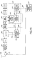
Images


Classifications
-
- H—ELECTRICITY
- H04—ELECTRIC COMMUNICATION TECHNIQUE
- H04L—TRANSMISSION OF DIGITAL INFORMATION, e.g. TELEGRAPHIC COMMUNICATION
- H04L27/00—Modulated-carrier systems
- H04L27/32—Carrier systems characterised by combinations of two or more of the types covered by groups H04L27/02, H04L27/10, H04L27/18 or H04L27/26
- H04L27/34—Amplitude- and phase-modulated carrier systems, e.g. quadrature-amplitude modulated carrier systems
- H04L27/36—Modulator circuits; Transmitter circuits
- H04L27/366—Arrangements for compensating undesirable properties of the transmission path between the modulator and the demodulator
- H04L27/367—Arrangements for compensating undesirable properties of the transmission path between the modulator and the demodulator using predistortion
Definitions
- the present invention relates to a distortion compensation address generator, a distortion compensating circuit, and a transmitter.
- a signal is radio transmitted from an antenna 503 through amplification due to an IF amplifier 501 and a transmitting amplifier 502.
- I/O (input/output) characteristic of the transmitting amplifier 502 it is ideal that a good linearity as shown in a dot-dash line of FIG. 17(b) is ensured.
- an amplification factor is reduced as input signal voltage increases higher because of a characteristic of a semiconductor element forming the transmitting amplifier 502, with the result that a non-linear distortion occurs. This distortion causes deterioration of communication quality.
- the distortion compensating circuit 500 compensates for transmitting data using compensation data having a characteristic opposite to the actual I/O characteristic of the transmitting amplifier (characteristic shown in the solid line of FIG. 17(b)), so that the linearity of transmitting amplifier 502 is improved.
- transmission power control is carried out for the purpose of reducing co-channel interference and power consumption of the mobile apparatus. If a gain of the transmitting amplifier is adjusted by the transmission power control, the compensation for the non-linear distortion must be carried out to follow the adjustment appropriately.
- transmission power of the transmitting amplifier varies over several tens of gradations (levels) by transmission power control. Therefore, the number of address generation tables corresponding to the number of gradations must be prepared. Moreover, in order to perform high-speed distortion compensation, it is necessary to operate the plurality of address generation tables. Therefore, in view of this point, there is difficulty in downsizing the communication apparatus and obtaining low power consumption.
- the present invention has been made in consideration of the above-mentioned problems, and an object of the present invention is to realize miniaturization of the circuit and low power consumption as ensuring high-speed distortion compensation of the transmitting amplifier.
- a distortion compensation address generator of the present invention in one preferred mode includes a plurality of comparators each for comparing a transmission power value with a respective predetermined reference value, a decoder for decoding an output of each of the plurality of comparators, and comparator control means for turning off a part of the plurality of comparators being not used in generation of the address, corresponding to a level of the transmission power value.
- comparator control means compares the transmission power value with an operation area coefficient prepared in advance so as to generate a control signal for turning off the part of the comparators.
- the comparison between the coefficient (operation area coefficient) prepared in advance and the transmission power value makes it possible to determine a comparator to be turned off in real time.
- the distortion compensation address generator of the present invention further comprises transmission power calculation means for calculating the transmission power value based on transmitting data.
- transmission power calculation means combines a plurality of transmitting signals to calculate transmission power.
- the address generator of the present invention can be used in not only a mobile apparatus for a cellular phone but also a base station apparatus.
- a distortion compensation address generator includes,
- the switching circuit turns on the address generation table when the transmission power is lower than a threshold value and turns on the address calculator when the transmission power is heigher than the threshold value.
- the address generation table In an address generation table with a comparator-off function, as the input power value is smaller, the effect of reduction in current consumption is brought to the fore. For this reason, the address generation table is used in an area where the input power value is smaller than the threshold value. Then, when the input power value exceeds the threshold value, the address calculator is used so as to restrain current consumption to be substantially constant regardless of an increase in the input power value. Thus, a synergistic effect therebetween makes it possible to restrain power consumption required in the address generation to a minimum. Also, the address generation table is not needed in an area where the input power value is great. For this reason, the number of comparators and that of decoders can be largely reduced, thereby achieving miniaturization of the apparatus.
- the address calculator has a function of executing an addition, a multiplication, and a division.
- the structure of the address calculator can be simplified.
- the address calculator performs the division by a bit shift operation. Since the division is performed by the bit shift operation, a divider can be basically formed by a shift register. Therefore, the structure of the address calculator can be further simplified.
- the distortion compensation address generator of the present invention further comprises transmission power calculation means for calculating the transmission power value based on transmitting data.
- transmission power calculation means combines a plurality of transmitting signals to calculate transmission power. Since transmission power can be calculated by combining the plurality of signals, the address generator of the present invention can be used in not only a mobile apparatus for a cellular phone but also a base station apparatus.
- a distortion compensation address generator includes,
- a plurality of address generation tables is prepared in response to transmission power control of the transmitting amplifier. Also, in a case where a plurality of pairs of calculation coefficient tables is built in the address calculator, only the table to be actually used is turned on in accordance with the level of transmission power and the other tables are turned off, thereby making it possible to largely reduce power consumption. After thus selecting the table to be used, the comparators unnecessary for the address generation table are turned off, and a change to the address calculator in a high transmission power area is carried out. As a result, power consumption necessary for the address generation can be further reduced, and the miniaturization of the apparatus can be achieved.
- transmission power calculation means combines a plurality of transmitting signals to calculate transmission power. Since transmission power can be calculated by combining the plurality of signals, the address generator of the present invention can be used in not only a mobile apparatus for a cellular phone but also a base station apparatus.
- the switching circuit turns on the address generation table when the transmission power is smaller than the threshold value and turns on the address calculator when the transmission power is larger than the threshold value.
- the address generation table In an address generation table with a comparator-off function, as the input power value is smaller, the effect of reduction in current consumption is brought to the fore. For this reason, the address generation table is used in an area where the input power value is smaller than the threshold value. Then, when the input power value exceeds the threshold value, the address calculator is used so as to restrain current consumption to be substantially constant regardless of an increase in the input power value. Thus, a synergistic effect therebetween makes it possible to restrain power consumption required in the address generation to a minimum. Also, the address generation table is not needed in an area where the input power value is large. For this reason, the number of comparators and that of decoders can be largely reduced, thereby achieving miniaturization of the apparatus.
- the address calculator has a function of executing an addition, a multiplication, and a division. Since the address is generated by a linear calculation, the structure of the address calculator can be simplified.
- the address calculator performs the division by a bit shift operation. Since the division is performed by the bit shift operation, a divider can be basically formed by a shift register. Therefore, the structure of the address calculator can be further simplified.
- a transmitter includes,
- a transmitter includes,
- a transmitter includes,
- the transmitter further comprises transmission power designating means for designating transmission power with respect to the transmitting amplifier and the distortion compensation address generator.
- transmission power designating means for designating transmission power with respect to the transmitting amplifier and the distortion compensation address generator.
- FIG. 1 is a circuit diagram showing the basic structure of a distortion compensation address generator according to this embodiment.
- the address generator comprises an input terminal 200 for transmission data, a power calculate section 201, a comparator control circuit 202, and an address generation table 203.
- the power calculate section 201 calculates a transmission power value.
- the calculation value of transmission power is one that is obtained by squaring each of input transmission data 1 to n and adding all resultant values or providing square root processing to the value of the addition.
- the comparator control circuit 202 determines a comparator to be operated based on the transmission power value, which is the calculation result of the power calculate section 201, and outputs a signal (comparator control signal), which is used to turn off an unnecessary comparator, to the address generation table 203.
- the address generation table 203 has numerous comparators, which are operable in parallel, built therein, and only necessary comparators are operated upon reception of the comparator control signal from the comparator control circuit 202. Then, the address generation table 203 performs operations such as comparison, decode, etc., using the transmission power value output from the power calculate section 201 as an input so as to generate an address for compensating distortion.
- the address for compensating distortion is output from an address output terminal 204.
- an address of a compensation data storing section 414 of FIG. 15 is designated, and non-linear distortion compensation data is output. Then, a compensation data multiply section 413 multiplies output data by transmission data, thereby obtaining corrected transmitting data. The entire system will be described later.
- transmitting signals of the respective channels Ich and Qch are input in parallel to the power calculate section 201.
- the input transmitting signals are squared by multipliers 111a and 111b, respectively, and added by an adder 112, respectively.
- Sequentially, these added signals are divided by a divider 114 using coefficient m of division stored in a register 113, and calculation results are output from a terminal 106.
- comparator control circuit 202 and address generation table 203 will be explained with reference to FIG. 3.
- the transmission power value is input to a terminal 205 provided at the comparator control circuit 202.
- the terminal 205 is a signal input terminal for a comparator 208.
- a coefficient storing section 207 a coefficient for selecting at least one comparator to be operated is stored.
- a decoder 209 generates control signals for comparators 221 to 228 of the address generation table 203 based on the comparison result of the comparator 208.
- the address generation table 203 has a comparison value group 211 including comparison value storing sections 212 to 219, which store comparison values "#0 to #7", respectively. Also, output terminals of comparison value storing sections 212 to 219 are connected to a comparator group 220 including comparators 221 to 228, respectively.
- the respective outputs of the comparator group 220 including comparators 221 to 228 are input to a decoder 229.
- the decoder 229 decodes input signals, and transmits the decoding result to an address storing section 230.
- the address storing section 230 is a memory, which stores an address showing an area where distortion compensation data of a transmitting amplifier is stored.
- the address storing section 230 is accessed by an output signal of the decoder 229, and outputs the address, which shows the area where distortion compensation data is stored, through an address output terminal 231.
- FIG. 4 shows an outline of the relationship between input power (transmission power calculation value) and current consumption of the address generator according to this embodiment.
- a characteristic A shown in a dash-single-dot line indicates a case (comparison) in which all comparators built in the address generation table 203 are always turned on, and a characteristic B shown in a solid line thereof indicates a case in which unnecessary comparators which do not substantially contribute to the address generation by control of the comparator control circuit 202.
- a characteristic B shown in a solid line thereof indicates a case in which unnecessary comparators which do not substantially contribute to the address generation by control of the comparator control circuit 202.
- FIG. 5(a) and FIG. 5(b) are views explaining the result of the effect of reduction in current consumption has been specifically examined by a computer simulation.
- FIG. 5(a) shows the results of which eight comparators #0 to #7 are turned on/off in accordance with the levels.
- comparators #0 to #7 are turned off, and current consumption corresponding to this range is reduced.
- a change in current consumption in this case is shown in FIG. 5(b).
- a noticeable reduction effect in consumption current is shown in an area where the transmission power calculation value is small.
- power consumption in the address generator can be reduced.
- the feature of this embodiment lies in the structure in which an address calculator is provided in addition to the address generation table as means for generating an address and both are switched in accordance with the transmission power value, whereby current consumption is reduced even in a higher transmission power area so as to realize higher reduction in power consumption than the previous embodiment.
- FIG. 6 is a block diagram showing the entire structure of a distortion compensation address generator.
- the address generator of this embodiment comprises a plurality (1 to n) of transmission data input terminals 240, a power calculate section 241, an address generation table (having comparator control circuit 202 shown in FIG. 3), an address calculator 243, an address generation switching device 244, an output selection circuit 245, and an address output terminal 246.
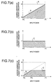
- FIGS. 7(a) to 7(c) are views explaining the principle of reduction in power consumption according to this embodiment.
- a characteristic A shows a case of the comparison
- a characteristic B shows a case of the address generation table with a comparator control function.
- an address generation table 242 with a comparator control function is used in a small input power area (characteristic B). Then, when input power exceeds a predetermined threshold value PC, the address calculator 243 is used (characteristic C). This controls an increase in current consumption even in an area where transmission power is high, so that current consumption can be more reduced as a whole in addition to the effect of reduction in current consumption obtained by turning off the comparator in the low power area.
- the occupation area of the circuit is suddenly increased even if the address calculator is newly added.
- the occupation area of the circuit forming the address generator can be reduced, and the apparatus can be downsized.
- transmission data n (1 to n) is input to the power calculate section 241.
- the calculation value of transmission power is one that is obtained by squaring each of input transmission data (1 to n) to n and adding all resultant values or providing square root processing to the value of the addition.
- the calculated transmission power values are input to the address generation table 242 and the address calculator 243 in parallel, respectively.
- the transmission power value is input to a switching device 244.
- the switching device 244 controls to operate either the address generation table 242 or the address calculator 243.
- An address generated by the address generation table 242 and an address generated by the address calculator 243 are sent to a selection circuit 245.
- the selection circuit 245 selects either the address supplied from the address generation table 242 or the address supplied from the address calculator 243 upon reception of a control signal from the switching device 244, and outputs the selected address to the address output terminal 246.
- a transmission power value which is input from an input terminal 250, is input to a comparator 251 provided in the switching device 244.
- a change-over threshold value memory 252 there is stored a transmission power value in a case where current consumption of the address generation table 242 exceeds current consumption of the address calculator 243.
- the transmission power value and a change-over threshold value 252 are input to the comparator 251, and a comparison result, serving as a change-over signal, is output from an output terminal 253.
- a change-over signal is input to a terminal 261 of the address calculator 243 from the switching device 244.
- the change-over signal functions as a control signal for turning on/off the address calculator 243. While, the transmission power is input to a terminal 260.
- a coefficient ⁇ for a multiplier is stored in a multiplication coefficient storing section 263.
- a coefficient ⁇ for an addition is stored in an adder coefficient storing section 265.
- a coefficient ⁇ for an addition is stored in an adder coefficient storing section 265.
- a coefficient ⁇ for an addition is stored in an adder coefficient storing section 265.
- a coefficient ⁇ for an addition is stored in a division coefficient storing section 267.
- a multiplier 262 multiplies the transmission power value by multiplication coefficient ⁇ .
- a signal showing the result is input to an adder 264, and coefficient ⁇ for an addition is added thereto.
- a signal showing the result is input to a divider 266, and a division using coefficient ⁇ for a division is executed here.
- a signal showing the result is input to a limiter circuit (LIM) 268, and a dynamic range for an output signal is limited here. Then, an address calculation result is output from an output terminal 269.
- LIM limiter circuit
- FIG. 9(b) shows the relationship between a transmission power value and an output address value.
- an address "#ad0" is output when the transmission power value is p0
- an address "#ad2" is output when the transmission power value is p2.
- FIG. 10(a) and FIG. 10(b) are views explaining the result of the reduction effect in current consumption of this embodiment, which has been specifically examined by a computer simulation.
- FIG. 10(a) shows the results of which eight comparators #0 to #7 are turned on/off in accordance with the levels and the result of "ON” and "OFF” determination of the address calculator 243.
- a part or all comparators #1 to #3 are turned on.
- the transmission power value exceeds "3”
- all comparators are turned off, and the address calculator 243 is turned on instead.
- FIG. 10(b) a change in current consumption is shown in FIG. 10(b).
- a diagonally shaded area which is enclosed with a characteristic line 270 (a characteristic due to the address generation table with a comparator address calculator) and a characteristic line 272 (a characteristic due to an address calculator), shows current consumption in this embodiment.
- the number of coparators, which are actually operated is small in the address generation table 242. For this reason, the number of built-in comparators can be reduced, and the occupation area of the circuit can be achieved at the same time.
- An address generator for compensating non-linear distortion is basically the same as the address generator explained in the second embodiment, and both are different from each other in a point that a division in the address calculator is carried out by use of a bit shift.
- FIG. 11 is a view showing the structure of the address calculator according to this embodiment.
- An address calculator 283 comprises signal input terminals 290, 291, a multiplier 292, an adder 294, coefficient storing sections 293, 295, 297, a bit shift circuit (shift register, etc.) 296, a limiter 298, and an address output terminal 299.
- bit shift circuit 296 Since digital data has a property in which a data value becomes 1/2 when being shift right by one bit, the bit shift circuit 296 easily performs the division through the use of this property.
- bit shift circuit 296 is basically structured by the shift register, there is an advantage in which the circuit can be simplified as compared with a case the divider is provided.
- the address for compensating distortion was only generated to follow transmission power, which instantaneously varied in accordance with the size of transmission data.
- an address for compensating distortion is generated in real time to follow a control value of transmission power control when the transmission power control is carried out for the purpose of reducing co-channel interference and power consumption of the mobile apparatus in a mobile communication system.
- transmission power control is carried out in the range of e.g., "-6dB” to "+24dB” by unit of 1dB, transmission power control of 31 levels in all is performed. Therefore, according to this embodiment, the address generation table and the calculation coefficient for an address calculator are prepared for each level. It should be noted that the basic structure is the same as the case of FIG. 6.
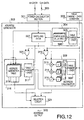
- FIG. 12 is a circuit diagram showing the structure of the address generator for compensating non-linear distortion according to this embodiment.
- one characteristic structure is that an address generation table 318 is provided in address generation table means 316 in accordance with each level (each gradation) of transmission power control and one of address generation tables is selected by a table change-over interface 317.
- the other characteristic structure is that a plurality of pairs of calculation coefficients ( ⁇ , ⁇ , ⁇ , etc.) are stored in coefficient storing sections 310 to 312 of an address calculator 308 and a pair of calculation coefficients (for example, ⁇ , ⁇ , ⁇ ) to be used is selected by a table change-over interface 309.
- the other characteristic structure is that there is provided a table change-over condition designating section 302 for outputting a control signal showing a table change-over condition based on a transmission power control value.
- a power calculate section 301 When transmission data (Ich, Qch) are input, a power calculate section 301 performs the calculation of the transmission power value. At this time, the calculation value of transmission power is one that is obtained by squaring each of input transmission data Ich and Qch and adding all resultant values or providing square root processing to the value of the addition.
- the table change-over condition designating section 302 stores a set value for transmission power control of a transmitting amplifier and outputs a control signal for performing a table change-over based on the set value.
- the control signal is input to an address generation change-over condition table 304, address generation table means 316, and the address calculator 308.
- These circuits have table change-over interfaces 305, 317, 309, respectively, and each of these table change-over interfaces 305, 317, 309 selects the table corresponding to the control level of transmission power and the coefficient, that is, the table and coefficient to be actually used.
- the address generation change-over condition table 304 has the table change-over interface 305 and a plurality of comparison value tables 306.
- the comparison value tables 306 store change values, which are necessary for determining on whether address generation table means 316 or the address calculator 308 is used in a selector 307.
- the selector 307 determines on whether address generation table means 316 or the address calculator 308 is used based on the transmission power calculation value, and outputs a change signal.
- the change signal output from the selector 307 and the control signal output from the table change-over condition designating section 302 are input to address generation table means 316 and the address calculator 308 through OR gates 320 and 319, respectively. By these signals, either address generation table means 316 or the address calculator 308 is turned on.
- address generation table means 316 In a case where address generation table means 316 is turned on, the transmission power calculation value is input to an address generation table 318 (table selected in accordance with a transmission power level), and an address for compensating distortion is output as a comparison result by the comparator and a decoding result of the decoder as previously explained.
- the address calculator 308 In a case where the address calculator 308 is turned on, as previously explained, calculations are carried out by a multiplier 313, an adder 314, and a divider 315 using a pair of calculation coefficients ⁇ , ⁇ , ⁇ (a pair of coefficients selected in accordance with the transmission power level) stored in the coefficient storing sections 310 to 312, and the address for compensating distortion is output as the calculation result.
- the address for compensating distortion is output from an output terminal 322 through an output selection circuit 321.
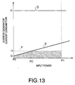
- the total number of comparators is 310 (31 x 10).
- the address generation table to be used is changed as required so that only the necessary address generation table is operated and only the necessary comparators built in the selected address are operated. As a result, current consumption in the address generation table is greatly reduced as shown in a characteristic line E of FIG. 13.
- the address generation using the address generation table is carried out.
- the address generation using the address calculator is carried out.
- a current consumption characteristic (the diagonally shaded area in the figure) in which characteristic lines E and F of FIG. 13 are combined is realized. This drastically reduces the total amount of current consumption.
- the reduction effect in current consumption according to this embodiment becomes more pronounces as the dynamic range of transmission power control is large and the level of the address to be output is finely set, so that a large effect can be obtained.
- the number of comparators to be built in one address generation table can be reduced, and the reduction effect can be obtained by being amplified by the number of levels (the number of gradations) of the transmission power control.
- the structure of the address calculator is simple. Therefore, according to this embodiment, the occupation area of the circuit is conspicuously reduced, and miniaturization of the apparatus can be improved.
- An address generator for compensating non-linear distortion is basically the same as the address generator explained in the fourth embodiment, and both are different from each other in a point that a division in the address calculator is carried out by use of a bit shift.
- FIG. 14 is a view showing the structure of the address generator for compensating non-linear distortion according to this embodiment.
- the point different from FIG. 13 is only the structure of an address calculator 330, and the other points are the same as the case of FIG. 13. Therefore, the same reference numerals as used in FIG. 13 are added to common portions.
- the address calculator 330 comprises a table change-over interface 331, calculation coefficient storing sections 332, 333, 334, a multiplier 335, an adder 336, and a bit shift circuit (shift register) 337. Since digital data has a property in which a data value becomes 1/2 when being shift right by one bit, the bit shift circuit 337 easily performs the division through the use of this property.
- bit shift circuit 337 is basically structured by the shift register and the structure is extremely simple, there is an advantage in which the circuit can be simplified as compared with a case the divider is provided.
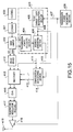
- FIG. 15 is a view showing the structure of a transmitter of a CDMA system using the address generator for compensating distortion according to the present invention.
- a portion closed with a dash-single-dot line is an address generator 403 for compensating distortion.
- a CODEC section 400 provides coding processing and transmission format forming processing to a transmitting signal.
- An output signal of CODEC section 400 is input to a CDMA section 401, and spread modulation processing using a spread code is provided here.
- a transmission band limiting section 402 wave-shapes the spread-modulated signal and provides band limitation processing thereto.
- a transmission power calculate section 404 provided in the address generator 403 squares the signals band-limited by the band limiter 402. Then, the transmission power calculate section 404 transmits a value, which is obtained by adding all resultant values or providing square root processing to the value of the addition, to an address generation section 409.
- a transmission power designating signal 407 output from a transmission power designating section 406 is input to a transmitting amplifier 418 and a table change-over determination section 405.
- the table change-over determination section 405 transmits a control signal for designating an address generation table, which is suitable for transmission power, to an address generation section 409.
- An address signal 410 generated from the address generation section 409 is input to a compensation data storing section 414, with the result that compensation data 415 is output. Compensation data is input to a compensation data multiply section 413.
- a delay device 412 has a function in which transmission is maintained and delayed by processing time required in the address generation section.
- An output of the delay device 412 is input to the compensation data multiply section 413. Then, complex multiplication processing using compensation data 415 sent from the compensation data storing section 414 is carried out. It should be noted that the control signal 410 to be sent to the compensation data storing section 414 from the address generation section 409 becomes active when the condition, which is shown by the output signal of the table change-over determination section 405, exceeds an normal operation range of the address generation section 409.
- the compensation data storing section 414 When the control signal 410 becomes active, the compensation data storing section 414 maintains a signal component, which has been output just before the control signal 410 becomes active, and stops the operation internally. The stop of operation cuts current consumed by the compensation data storing section 414 and contributes to reduction in power consumption.
- a D/A converter 416 converts transmitting data complex multiplied by the compensation data multiply section 413 to an analog signal.
- An output signal of the D/A converter 416 is subjected to quadrature modulation processing by a quadrature modulation section 417 and sent to a transmitting amplifier 418.
- An output amplified by the transmitting amplifier 418 is transmitted through an antenna 419.
- FIG. 16 is a view showing the structure of a transmitter of a TDMA system using the address generator for compensating distortion according to the present invention.
- a portion enclosed with a dash-single-dot line (reference numeral 453) is the distortion compensation address generator according to the present invention.
- data to which coding processing is provided by a CODEC-section 450 is input to a TDMA section 451 so as to be reconstructed to a transmission format of TDMA.
- a transmission band limiting section 452 wave-shapes a spread-modulated signal and provides a predetermined band limitation thereto.
- a transmission power calculate section 454 provided in an address generator 453 squares two output signals of the band limiter 452. Then, the transmission power calculate section 454 outputs a value, which is obtained by adding all resultant values or providing square root processing to the value of the addition, to be transmitted to an address generation section 459.
- a transmission power designating signal 457 output from a transmission power designating section 456 is input to a transmitting amplifier 468 and a table change-over determination section 455.
- the table change-over determination section 455 generates a signal 458 for controlling the address generation table of an address generation section 459 and the operation of the address calculator, and transmits the signal.
- a predetermined address for a compensation data storing section 464 is designated by an address signal 461 output from the address generation section 459, and compensation data 465 stored at the designated address is transmitted to a compensation data multiply section 463.
- a control signal 460 output from the address generation section 464 is a signal for controlling ON/Off of the circuit of the compensation data storing section 464.
- the control signal 460 becomes active when the condition, which is shown by the output signal of the table change-over determination section 455, exceeds an normal operation range of the address generation section 459.
- the compensation data storing section 464 maintains a signal component, which has been output just before the control signal 460 becomes active, and stops the operation internally. The stop of operation can prevent waste power consumption.
- a delay device 462 has a function in which transmission is maintained by processing time required in the address generation section 459.
- An output of the delay device 462 is input to the compensation data multiply section 463. Then, complex multiplication processing is carried out using compensation data 465.
- a D/A converter 466 converts transmitting data complex multiplied by the compensation data multiply section 463 to an analog signal.
- An output signal of the D/A converter 466 is subjected to quadrature modulation processing by quadrature modulation section 467 and amplified by a transmitting amplifier 468, and transmitted through an antenna 469.
- circuit for compensating an instantaneous variation in the transmission power value, control such that a minimum current consumption can be attained is always carried out. Also, at the time of compensating for a variation in the control value of transmission power control of the transmitting amplifier, circuit can be controlled such that a minimum current consumption can be attained is always carried out.
- the circuit of the present invention is suitable for an IC implementation for the reason of low power consumption. Moreover, this contributes to the miniaturization of the communication apparatus and the use for a long time.
Landscapes
- Engineering & Computer Science (AREA)
- Computer Networks & Wireless Communication (AREA)
- Signal Processing (AREA)
- Transmitters (AREA)
- Amplifiers (AREA)
- Control Of Amplification And Gain Control (AREA)
Applications Claiming Priority (2)
| Application Number | Priority Date | Filing Date | Title |
|---|---|---|---|
| JP19771998 | 1998-07-13 | ||
| JP19771998A JP3360029B2 (ja) | 1998-07-13 | 1998-07-13 | 歪補償用アドレス発生器,歪補償回路および送信歪補償付き送信機 |
Publications (2)
| Publication Number | Publication Date |
|---|---|
| EP0973307A2 true EP0973307A2 (de) | 2000-01-19 |
| EP0973307A3 EP0973307A3 (de) | 2006-11-02 |
Family
ID=16379223
Family Applications (1)
| Application Number | Title | Priority Date | Filing Date |
|---|---|---|---|
| EP99113713A Withdrawn EP0973307A3 (de) | 1998-07-13 | 1999-07-13 | Verzerrungskompensationssystem |
Country Status (3)
| Country | Link |
|---|---|
| US (1) | US6272326B1 (de) |
| EP (1) | EP0973307A3 (de) |
| JP (1) | JP3360029B2 (de) |
Cited By (2)
| Publication number | Priority date | Publication date | Assignee | Title |
|---|---|---|---|---|
| WO2004064248A1 (en) * | 2003-01-13 | 2004-07-29 | Telefonaktiebolaget L M Ericsson (Publ) | Device and method for predistorting an input signal |
| EP1455444A1 (de) * | 2003-01-13 | 2004-09-08 | Telefonaktiebolaget LM Ericsson (publ) | Vorrichtung und Verfahren zum Vorverzerrung eines Eingangssignals |
Families Citing this family (8)
| Publication number | Priority date | Publication date | Assignee | Title |
|---|---|---|---|---|
| JP3381689B2 (ja) * | 1999-11-30 | 2003-03-04 | 日本電気株式会社 | 非線形歪み補償回路及びそれを用いた送信装置並びに移動通信機 |
| US6968258B2 (en) * | 2002-05-31 | 2005-11-22 | Texas Instruments Incorporated | Residual feedback to improve estimator prediction |
| EP1511181B1 (de) | 2002-05-31 | 2009-12-09 | Fujitsu Limited | Verzerrungskompensator |
| EP1503333A1 (de) * | 2003-08-01 | 2005-02-02 | Sony International (Europe) GmbH | Korrektur uneinheitlicher Bildwiedergabe |
| US7895378B2 (en) * | 2004-04-27 | 2011-02-22 | Apple Inc. | Method and system for allowing a media player to transfer digital audio to an accessory |
| JP4845574B2 (ja) * | 2005-04-26 | 2011-12-28 | パナソニック株式会社 | 極座標変調回路、集積回路および無線装置 |
| JP4634328B2 (ja) * | 2006-03-30 | 2011-02-16 | 京セラ株式会社 | 増幅装置、送信装置、端末装置、及び基地局装置 |
| US8983639B2 (en) * | 2008-12-14 | 2015-03-17 | Apple Inc. | Techniques for facilitating interoperation between a host device and a digital RF tuner accessory |
Family Cites Families (10)
| Publication number | Priority date | Publication date | Assignee | Title |
|---|---|---|---|---|
| DE3417776A1 (de) * | 1983-06-01 | 1985-11-21 | Manfred Dipl.-Ing. 7000 Stuttgart Horn | Verfahren und schaltungsanordnungen zur kompensation von nichtlinearen amplituden- und/oder phasenverzerrungen |
| US5778029A (en) * | 1993-05-13 | 1998-07-07 | Lockheed Martin Aerospace Corporation | Signal conditioner with symbol addressed lookup table producing values which compensate linear and non-linear distortion using transversal filter |
| US5574967A (en) * | 1994-01-11 | 1996-11-12 | Ericsson Ge Mobile Communications, Inc. | Waste energy control and management in power amplifiers |
| JPH0974371A (ja) | 1995-09-05 | 1997-03-18 | Hitachi Denshi Ltd | 無線機 |
| FR2746564B1 (fr) * | 1996-03-22 | 1998-06-05 | Matra Communication | Procede pour corriger des non-linearites d'un amplificateur, et emetteur radio mettant en oeuvre un tel procede |
| FR2746563B1 (fr) * | 1996-03-22 | 1998-06-05 | Matra Communication | Procede pour corriger des non-linearites d'un amplificateur, et emetteur radio mettant en oeuvre un tel procede |
| US5898338A (en) * | 1996-09-20 | 1999-04-27 | Spectrian | Adaptive digital predistortion linearization and feed-forward correction of RF power amplifier |
| US5923712A (en) * | 1997-05-05 | 1999-07-13 | Glenayre Electronics, Inc. | Method and apparatus for linear transmission by direct inverse modeling |
| US6072364A (en) * | 1997-06-17 | 2000-06-06 | Amplix | Adaptive digital predistortion for power amplifiers with real time modeling of memoryless complex gains |
| US6081158A (en) * | 1997-06-30 | 2000-06-27 | Harris Corporation | Adaptive pre-distortion apparatus for linearizing an amplifier output within a data transmission system |
-
1998
- 1998-07-13 JP JP19771998A patent/JP3360029B2/ja not_active Expired - Fee Related
-
1999
- 1999-07-12 US US09/351,170 patent/US6272326B1/en not_active Expired - Fee Related
- 1999-07-13 EP EP99113713A patent/EP0973307A3/de not_active Withdrawn
Cited By (2)
| Publication number | Priority date | Publication date | Assignee | Title |
|---|---|---|---|---|
| WO2004064248A1 (en) * | 2003-01-13 | 2004-07-29 | Telefonaktiebolaget L M Ericsson (Publ) | Device and method for predistorting an input signal |
| EP1455444A1 (de) * | 2003-01-13 | 2004-09-08 | Telefonaktiebolaget LM Ericsson (publ) | Vorrichtung und Verfahren zum Vorverzerrung eines Eingangssignals |
Also Published As
| Publication number | Publication date |
|---|---|
| US6272326B1 (en) | 2001-08-07 |
| JP2000031840A (ja) | 2000-01-28 |
| JP3360029B2 (ja) | 2002-12-24 |
| EP0973307A3 (de) | 2006-11-02 |
Similar Documents
| Publication | Publication Date | Title |
|---|---|---|
| US6944469B2 (en) | Apparatus and method for controlling transmission power in a mobile communication system | |
| EP1303053A1 (de) | Verfahren und Einrichtung zur kontinuierlichen Steuerung des dynamischen Bereichs eines Analog-Digital-Wandlers | |
| US6272326B1 (en) | Distortion compensation address generator, distortion compensating circuit, and transmitter | |
| KR100314334B1 (ko) | 디지털 자동 이득 제어용 리니어라이저 및 이것을 이용한 디지털 자동 이득 제어 회로 | |
| US6351462B1 (en) | CDMA receiving apparatus and method therefor | |
| JPH07202775A (ja) | ダイバーシティ受信信号合成回路 | |
| US7127268B2 (en) | Radio transmission apparatus and radio transmission method | |
| US7031289B1 (en) | Control of amplitude level of baseband signal to be transmitted on the basis of the number of transmission codes | |
| US20020160801A1 (en) | Radio communication apparatus and transmission power control method | |
| GB2336260A (en) | Gain control in a CDMA receiver in which, if the deviation is greater than a set amount, the feedback is adjusted to increase the speed of convergence | |
| EP0924875B1 (de) | Verfahren und Vorrichtung zum Diversity-Empfang in einem CDMA-System | |
| EP1081851A2 (de) | Begrenzungsverfahren und Begrenzervorrichtung | |
| EP0941584B1 (de) | Verfahren zur übertragungsoptimierung und sender | |
| EP1108285B1 (de) | Regelung von leistungsverhältnissen für in-phase und quadrature kanäle in einem kommunikationssystem | |
| JP4515481B2 (ja) | デジタル通信システムにおける量子化装置及び方法 | |
| KR101042807B1 (ko) | 주파수 직접변환 방식 수신기의 부정합 보상 장치 및 방법 | |
| KR100383505B1 (ko) | 코드 분할 다중 액세스 무선전화기용 디지탈 자동 이득 제어 방법 및 장치 | |
| JP2001086048A (ja) | ダイバ−シチ受信機 | |
| JP2003078503A (ja) | 平均化演算方法および平均電力演算装置 | |
| GB2407222A (en) | Gain control amplification circuit for CDMA terminal |
Legal Events
| Date | Code | Title | Description |
|---|---|---|---|
| PUAI | Public reference made under article 153(3) epc to a published international application that has entered the european phase |
Free format text: ORIGINAL CODE: 0009012 |
|
| AK | Designated contracting states |
Kind code of ref document: A2 Designated state(s): AT BE CH CY DE DK ES FI FR GB GR IE IT LI LU MC NL PT SE |
|
| AX | Request for extension of the european patent |
Free format text: AL;LT;LV;MK;RO;SI |
|
| PUAL | Search report despatched |
Free format text: ORIGINAL CODE: 0009013 |
|
| AK | Designated contracting states |
Kind code of ref document: A3 Designated state(s): AT BE CH CY DE DK ES FI FR GB GR IE IT LI LU MC NL PT SE |
|
| AX | Request for extension of the european patent |
Extension state: AL LT LV MK RO SI |
|
| 17P | Request for examination filed |
Effective date: 20061207 |
|
| AKX | Designation fees paid |
Designated state(s): DE FR GB NL |
|
| 17Q | First examination report despatched |
Effective date: 20070824 |
|
| GRAP | Despatch of communication of intention to grant a patent |
Free format text: ORIGINAL CODE: EPIDOSNIGR1 |
|
| RAP1 | Party data changed (applicant data changed or rights of an application transferred) |
Owner name: PANASONIC CORPORATION |
|
| STAA | Information on the status of an ep patent application or granted ep patent |
Free format text: STATUS: THE APPLICATION IS DEEMED TO BE WITHDRAWN |
|
| 18D | Application deemed to be withdrawn |
Effective date: 20090114 |