EP0973204B1 - Verfahren zur Herstellung einer MOS-Transistoranordnung - Google Patents
Verfahren zur Herstellung einer MOS-Transistoranordnung Download PDFInfo
- Publication number
- EP0973204B1 EP0973204B1 EP99112270A EP99112270A EP0973204B1 EP 0973204 B1 EP0973204 B1 EP 0973204B1 EP 99112270 A EP99112270 A EP 99112270A EP 99112270 A EP99112270 A EP 99112270A EP 0973204 B1 EP0973204 B1 EP 0973204B1
- Authority
- EP
- European Patent Office
- Prior art keywords
- mos transistor
- implantation
- drain
- region
- drain extension
- Prior art date
- Legal status (The legal status is an assumption and is not a legal conclusion. Google has not performed a legal analysis and makes no representation as to the accuracy of the status listed.)
- Expired - Lifetime
Links
Images
Classifications
-
- H—ELECTRICITY
- H10—SEMICONDUCTOR DEVICES; ELECTRIC SOLID-STATE DEVICES NOT OTHERWISE PROVIDED FOR
- H10D—INORGANIC ELECTRIC SEMICONDUCTOR DEVICES
- H10D30/00—Field-effect transistors [FET]
- H10D30/01—Manufacture or treatment
- H10D30/021—Manufacture or treatment of FETs having insulated gates [IGFET]
- H10D30/0221—Manufacture or treatment of FETs having insulated gates [IGFET] having asymmetry in the channel direction, e.g. lateral high-voltage MISFETs having drain offset region or extended-drain MOSFETs [EDMOS]
-
- H—ELECTRICITY
- H10—SEMICONDUCTOR DEVICES; ELECTRIC SOLID-STATE DEVICES NOT OTHERWISE PROVIDED FOR
- H10D—INORGANIC ELECTRIC SEMICONDUCTOR DEVICES
- H10D30/00—Field-effect transistors [FET]
- H10D30/60—Insulated-gate field-effect transistors [IGFET]
- H10D30/601—Insulated-gate field-effect transistors [IGFET] having lightly-doped drain or source extensions, e.g. LDD IGFETs or DDD IGFETs
- H10D30/603—Insulated-gate field-effect transistors [IGFET] having lightly-doped drain or source extensions, e.g. LDD IGFETs or DDD IGFETs having asymmetry in the channel direction, e.g. lateral high-voltage MISFETs having drain offset region or extended drain IGFETs [EDMOS]
-
- H—ELECTRICITY
- H10—SEMICONDUCTOR DEVICES; ELECTRIC SOLID-STATE DEVICES NOT OTHERWISE PROVIDED FOR
- H10D—INORGANIC ELECTRIC SEMICONDUCTOR DEVICES
- H10D62/00—Semiconductor bodies, or regions thereof, of devices having potential barriers
- H10D62/10—Shapes, relative sizes or dispositions of the regions of the semiconductor bodies; Shapes of the semiconductor bodies
- H10D62/13—Semiconductor regions connected to electrodes carrying current to be rectified, amplified or switched, e.g. source or drain regions
- H10D62/149—Source or drain regions of field-effect devices
- H10D62/151—Source or drain regions of field-effect devices of IGFETs
-
- H—ELECTRICITY
- H10—SEMICONDUCTOR DEVICES; ELECTRIC SOLID-STATE DEVICES NOT OTHERWISE PROVIDED FOR
- H10D—INORGANIC ELECTRIC SEMICONDUCTOR DEVICES
- H10D84/00—Integrated devices formed in or on semiconductor substrates that comprise only semiconducting layers, e.g. on Si wafers or on GaAs-on-Si wafers
- H10D84/01—Manufacture or treatment
- H10D84/0123—Integrating together multiple components covered by H10D12/00 or H10D30/00, e.g. integrating multiple IGBTs
- H10D84/0126—Integrating together multiple components covered by H10D12/00 or H10D30/00, e.g. integrating multiple IGBTs the components including insulated gates, e.g. IGFETs
- H10D84/013—Manufacturing their source or drain regions, e.g. silicided source or drain regions
-
- H—ELECTRICITY
- H10—SEMICONDUCTOR DEVICES; ELECTRIC SOLID-STATE DEVICES NOT OTHERWISE PROVIDED FOR
- H10D—INORGANIC ELECTRIC SEMICONDUCTOR DEVICES
- H10D84/00—Integrated devices formed in or on semiconductor substrates that comprise only semiconducting layers, e.g. on Si wafers or on GaAs-on-Si wafers
- H10D84/01—Manufacture or treatment
- H10D84/02—Manufacture or treatment characterised by using material-based technologies
- H10D84/03—Manufacture or treatment characterised by using material-based technologies using Group IV technology, e.g. silicon technology or silicon-carbide [SiC] technology
- H10D84/038—Manufacture or treatment characterised by using material-based technologies using Group IV technology, e.g. silicon technology or silicon-carbide [SiC] technology using silicon technology, e.g. SiGe
-
- H—ELECTRICITY
- H10—SEMICONDUCTOR DEVICES; ELECTRIC SOLID-STATE DEVICES NOT OTHERWISE PROVIDED FOR
- H10D—INORGANIC ELECTRIC SEMICONDUCTOR DEVICES
- H10D84/00—Integrated devices formed in or on semiconductor substrates that comprise only semiconducting layers, e.g. on Si wafers or on GaAs-on-Si wafers
- H10D84/80—Integrated devices formed in or on semiconductor substrates that comprise only semiconducting layers, e.g. on Si wafers or on GaAs-on-Si wafers characterised by the integration of at least one component covered by groups H10D12/00 or H10D30/00, e.g. integration of IGFETs
- H10D84/82—Integrated devices formed in or on semiconductor substrates that comprise only semiconducting layers, e.g. on Si wafers or on GaAs-on-Si wafers characterised by the integration of at least one component covered by groups H10D12/00 or H10D30/00, e.g. integration of IGFETs of only field-effect components
- H10D84/83—Integrated devices formed in or on semiconductor substrates that comprise only semiconducting layers, e.g. on Si wafers or on GaAs-on-Si wafers characterised by the integration of at least one component covered by groups H10D12/00 or H10D30/00, e.g. integration of IGFETs of only field-effect components of only insulated-gate FETs [IGFET]
-
- H—ELECTRICITY
- H10—SEMICONDUCTOR DEVICES; ELECTRIC SOLID-STATE DEVICES NOT OTHERWISE PROVIDED FOR
- H10D—INORGANIC ELECTRIC SEMICONDUCTOR DEVICES
- H10D84/00—Integrated devices formed in or on semiconductor substrates that comprise only semiconducting layers, e.g. on Si wafers or on GaAs-on-Si wafers
- H10D84/80—Integrated devices formed in or on semiconductor substrates that comprise only semiconducting layers, e.g. on Si wafers or on GaAs-on-Si wafers characterised by the integration of at least one component covered by groups H10D12/00 or H10D30/00, e.g. integration of IGFETs
- H10D84/82—Integrated devices formed in or on semiconductor substrates that comprise only semiconducting layers, e.g. on Si wafers or on GaAs-on-Si wafers characterised by the integration of at least one component covered by groups H10D12/00 or H10D30/00, e.g. integration of IGFETs of only field-effect components
- H10D84/83—Integrated devices formed in or on semiconductor substrates that comprise only semiconducting layers, e.g. on Si wafers or on GaAs-on-Si wafers characterised by the integration of at least one component covered by groups H10D12/00 or H10D30/00, e.g. integration of IGFETs of only field-effect components of only insulated-gate FETs [IGFET]
- H10D84/836—Integrated devices formed in or on semiconductor substrates that comprise only semiconducting layers, e.g. on Si wafers or on GaAs-on-Si wafers characterised by the integration of at least one component covered by groups H10D12/00 or H10D30/00, e.g. integration of IGFETs of only field-effect components of only insulated-gate FETs [IGFET] comprising EDMOS
-
- H—ELECTRICITY
- H10—SEMICONDUCTOR DEVICES; ELECTRIC SOLID-STATE DEVICES NOT OTHERWISE PROVIDED FOR
- H10D—INORGANIC ELECTRIC SEMICONDUCTOR DEVICES
- H10D64/00—Electrodes of devices having potential barriers
- H10D64/20—Electrodes characterised by their shapes, relative sizes or dispositions
- H10D64/27—Electrodes not carrying the current to be rectified, amplified, oscillated or switched, e.g. gates
- H10D64/311—Gate electrodes for field-effect devices
- H10D64/411—Gate electrodes for field-effect devices for FETs
- H10D64/511—Gate electrodes for field-effect devices for FETs for IGFETs
- H10D64/514—Gate electrodes for field-effect devices for FETs for IGFETs characterised by the insulating layers
- H10D64/516—Gate electrodes for field-effect devices for FETs for IGFETs characterised by the insulating layers the thicknesses being non-uniform
-
- H—ELECTRICITY
- H10—SEMICONDUCTOR DEVICES; ELECTRIC SOLID-STATE DEVICES NOT OTHERWISE PROVIDED FOR
- H10D—INORGANIC ELECTRIC SEMICONDUCTOR DEVICES
- H10D84/00—Integrated devices formed in or on semiconductor substrates that comprise only semiconducting layers, e.g. on Si wafers or on GaAs-on-Si wafers
- H10D84/80—Integrated devices formed in or on semiconductor substrates that comprise only semiconducting layers, e.g. on Si wafers or on GaAs-on-Si wafers characterised by the integration of at least one component covered by groups H10D12/00 or H10D30/00, e.g. integration of IGFETs
- H10D84/82—Integrated devices formed in or on semiconductor substrates that comprise only semiconducting layers, e.g. on Si wafers or on GaAs-on-Si wafers characterised by the integration of at least one component covered by groups H10D12/00 or H10D30/00, e.g. integration of IGFETs of only field-effect components
- H10D84/83—Integrated devices formed in or on semiconductor substrates that comprise only semiconducting layers, e.g. on Si wafers or on GaAs-on-Si wafers characterised by the integration of at least one component covered by groups H10D12/00 or H10D30/00, e.g. integration of IGFETs of only field-effect components of only insulated-gate FETs [IGFET]
- H10D84/83138—Integrated devices formed in or on semiconductor substrates that comprise only semiconducting layers, e.g. on Si wafers or on GaAs-on-Si wafers characterised by the integration of at least one component covered by groups H10D12/00 or H10D30/00, e.g. integration of IGFETs of only field-effect components of only insulated-gate FETs [IGFET] the IGFETs characterised by having different shapes or dimensions of their gate conductors
Definitions
- the invention relates to a method for producing a MOS transistor arrangement having a high-voltage (HV) MOS transistor with a low on-resistance and a low-voltage logic MOS transistor.
- HV high-voltage
- NMOS transistors are known in which a buried layer (below a drain extension region) Buried layer) is arranged. The dopant concentration of the buried layer is higher than the dopant concentration within the drain extension region. This results, starting from the substrate surface, in the depth extent of the substrate, a retrograde Dotierstoffkonzentrationsprofil.
- the currently used HV-NMOS transistors with a blocking voltage of up to about 150 volts are unprofitable in terms of area due to the voltage-optimized design for voltage ranges around 20 volts.
- the diffused n-well used there as a drain extension (FIG. 1) also in conjunction with a field plate (FIG. 2), represents the classical approach for increasing the dielectric strength. Since this n-well has been designed in its doping such that it is suitable for receiving the complementary transistor (PMOS), their doping is at a rather low level. When used as a drain extension, this has a limiting effect on the performance of the transistor in terms of the current yield.
- the existing NMOS logic transistor is optimized for just this current yield, but does not have the necessary dielectric strength.
- HV transistors for voltages greater than 30 volts are also realized. These are optimized for the 30/40/50 Volt peak voltages common in the automotive industry, but also for the suppression of interference pulses up to about 150 volts. Also, the voltage range 10 volts to 30 volts is currently covered with these HV transistors due to non-existent special transistors. With specially optimized transistors for this voltage range a higher performance and thus a surface spatter should be achieved.
- the invention has for its object to provide a method for producing a MOS transistor arrangement with a high-voltage MOS transistor with high To provide voltage resistance and low on-resistance and a logic MOS transistor, wherein the high-voltage MOS transistor can be produced using required for the logic MOS transistor process steps.
- the invention proposes a MOS transistor arrangement with a high-voltage MOS transistor with high dielectric strength and low on-resistance and a logic MOS transistor according to claim 1.
- the drain extension region required to increase the withstand voltage is generated by an ion implantation step, wherein the implant has a lower dopant concentration in its top side near the top of the substrate than in its region below it near-top area.
- the drain extension region has a so-called retrograde profile.
- This has the advantage that an implanted retrograde well can be used as the drain extension, as is used for the low-power transistor (logic transistor) of the inventive arrangement in typical submicron technologies.
- This can be used for producing the high-voltage MOS transistor according to the invention process steps, as they are currently used for the production of integrated low-voltage MOS logic transistors.
- the process control remains unchanged and in particular is not extended by additional process steps. In particular, the thermal budget remains unchanged.
- the drain extension region is realized by means of a two- or three-step implantation process, wherein as second and / or third implantation known from low-voltage transistors forth ion implantations for threshold adjustment and to prevent a punch-through Effect can be used.
- HV-MOS transistor of the arrangement according to the invention Another advantage of the HV-MOS transistor of the arrangement according to the invention is to be seen in the fact that an increased performance with reduced space requirement is achieved.
- the current efficiency of the HV transistor according to the invention is improved, whereas the dielectric strength is somewhat limited due to the less soft doping processes in the corner regions of the retrograde implantation profile.
- the withstand voltage is sufficient for the requirements applicable in the automotive sector, so that in the case of the transistor according to the invention, it is preferable to reduce the space required.
- the essential innovation of the MOS transistor arrangement produced according to the invention is therefore to be seen in the use of a retrograde well profile for generating the drain extension of the HV MOS transistor, so that the retrograde wells optimized for the low-voltage logic transistors can be used as a drain extension for high-voltage components, thereby both an unchanged and simple process results without additional steps.
- PCT application PCT / EP96 / 04246, publication number WO-A-97/13277 PCT application PCT / EP96 / 04246, publication number WO-A-97/13277.
- This method can also be applied to the components described above, which is why the content of the PCT application is also made the subject of the present application.
- the described new components can not be realized only as a type n-channel.
- the feasibility of the type p-channel is also possible by using the p-low-voltage well as a drain extension within the existing HV-n-tub as a body.
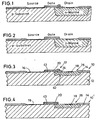
- Fig. 3 shows a longitudinal section through a first embodiment of a MOS transistor 10 of the inventive arrangement, which is a NMOS acts.
- the MOS transistor 10 is formed in a p-doped substrate 12 whose active region is defined by an opening in a field oxide layer 14.
- the NMOS transistor 10 has degenerately n-doped source and drain regions 16, 18, between which a gate electrode 20 is arranged.
- the gate electrode 20 has a drain-side end region 22 facing the drain region 18, below which a field plate 24 made of silicon oxide is arranged.
- the drain region 18 is located in a drain extension region 26 that is created by ion implantation.
- This ion implantation is the implantation that is also used to form a well within the substrate 12 within which is then formed a NMOS low-voltage logic transistor.
- a logic transistor is shown at 30 in FIG.
- the drain extension region 26 is n-doped and has an increasing dopant concentration with increasing depth.
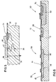
- creates a retrograde tub profile which is shown in Fig. 5.
- the dopant concentration is plotted versus the depth plotted along the axis 34.
- the dopant concentration profile 36 which is spaced from the substrate surface 38 in the near-surface region of the substrate 12, is due to the implantation process for introducing a well region in the substrate, such a well region also being required in the formation of the logic transistor 30.
- the field plate 24 already formed upon introduction of this implantation results in implantation not penetrating into the substrate 12 as far below the field plate 24 as outside the field plate 24. This is illustrated in FIG.
- transistor 10 of FIG. 3 and 5 add a second implantation step, namely the implantation step for introducing an anti-punch-through implantation.
- the resulting dopant concentration profile is shown at 42 in FIG.
- This Implantation step is less energetic than the first described and performed implantation step, which is why the dopant concentration profile 42 is formed in the region between the profile 36 and the substrate surface 28, the energy is so low that the ion implantation does not penetrate the field plate 24 and thus only forms below the gate electrode 20.
- This anti-punch-through implantation is needed at the logic transistor 30 to limit expansion of the space charge region of the drain region 44 of the logic transistor 30 toward the source region 46.
- a further ion implantation step may be performed, the one for setting the turn-on threshold (threshold setting) of the logic transistor 30.
- This implantation step is also introduced into the drain extension region 26, wherein the dopant concentration caused thereby on the substrate surface 38 has an effect. In Fig. 5, the dopant concentration profile caused thereby is not shown.
- the drain extension region 26 of the HV transistor 10 is thereby produced by up to three implantation steps, wherein an increasing doping concentration with increasing depth within the channel region 48 occurs.
- the low-resistance connection of the drain extension region 26 to the channel region 48 takes place.
- FIG. 4 shows an alternative exemplary embodiment of an NMOS transistor 10 'of the arrangement produced according to the invention, which, except for the field plate 24, is identical to the NMOS transistor 10 according to FIG. 3.
- this field plate 24 is missing; this affects the dopant concentration distribution within the drain extension region 26, ultimately resulting in the voltage resistance of the transistor 10 'being slightly reduced from the withstand voltage of the transistor 10.
- due to the field plate 24 also within the region 26 results in a retrograde doping profile, whereby the flow of current between the channel region 48 below the gate electrode 20 and the drain region 18 does not take place exclusively at the surface but predominantly in the volume of the drain extension region 26, that is, at its depth. This has the advantage that the current flow is not affected by surface effects and thus more reliable and reproducible.
- Fig. 6 finally shows the formation of inventively prepared MOS transistor arrangements with logic transistors and HV transistors in the same substrate 12. It can be seen that the drain extension region 26 of the HV-NMOS transistor 10 as an active region 49 for the logic NMOS transistor 30 is used. When the invention is used with an HV PMOS transistor 50 formed within an HV-n well 52 of the substrate 12, the drain extension region 54 of this HV PMOS transistor 50 corresponds to the well 56 of one in the p-type well. Substrate 12 integrated logic PMOS transistor 58th
Landscapes
- Metal-Oxide And Bipolar Metal-Oxide Semiconductor Integrated Circuits (AREA)
- Insulated Gate Type Field-Effect Transistor (AREA)
Description
- Die Erfindung betrifft ein Verfahren zur Herstellung einer MOS-Transistoranordnung mit einem Hochvolt-(HV-)MOS-Transistor mit niedrigem Einschaltwiderstand und einem Niedervolt-Logik-MOS-Transistor.
- Aus ALIAHMAD M ET AL: 'A SHORT LOOP SLIC IN A SUBMICRON BICMOS TECHNOLOGY' IEEE INTERNATIONAL SYMPOSIUM ON POWER SEMICONDUCTOR DEVICES AND ICS,US,NEW YORK, NY: IEEE, Bd. CONF. 9, 26. Mai 1997 (1997-05-26), Seiten 329-332, XP000800213 ISBN: 0-7803-3994-0 und RAMEZANI M ET AL: 'A MONOLITHIC IGBT GATE DRIVER IMPLEMENTED IN A CONVENTIONAL 0.8MUM BICMOS PROCESS' KYOTO, JUNE 3-6, 1998,NEW YORK; NY: IEEE,US, 3. Juni 1998 (1998-06-03), Seiten 109-112, XP000801044 ISBN: 0-7803-4752-8 sind NMOS-Transistoren bekannt, bei denen unterhalb eines Drainextension-Gebietes eine vergrabene Schicht (buried layer) angeordnet ist. Die Dotierstoffkonzentration der vergrabenen Schicht ist höher als die Dotierstoffkonzentration innerhalb des Drainextension-Gebietes. Damit ergibt sich, ausgehend von der Substratoberfläche, in Tiefenerstreckung des Substrats ein retrogrades Dotierstoffkonzentrationsprofil.
- Die derzeit verwendeten HV-NMOS-Transistoren mit einer Sperrspannung von bis zu ca. 150 Volt sind aufgrund der spannungsoptimierten Konstruktion für Spannungsbereiche um 20 Volt flächenmäßig unrentabel. Die dort verwendete diffundierte n-Wanne als Drainextension (Fig. 1), auch in Verbindung mit einer Feldplatte (Fig. 2), stellt den klassischen Ansatz zur Erhöhung der Spannungsfestigkeit dar. Da diese n-Wanne in ihrer Dotierung so ausgelegt wurde, dass sie zur Aufnahme des Komplementärtransistors (PMOS) geeignet ist, liegt ihre Dotierung auf einem eher niedrigen Niveau. Diese wirkt bei Verwendung als Drainextension limitierend für die Performance des Transistors in Bezug auf die Stromergiebigkeit.
- Der vorhandene NMOS-Logiktransistor dagegen ist auf gerade diese Stromergiebigkeit optimiert, verfügt aber nicht über die notwendige Spannungsfestigkeit.
- In CMOS-Prozessen werden neben Logiktransistoren für den 5 Volt Spannungsbereich auch HV-Transistoren für Spannungen größer 30 Volt realisiert. Diese sind auf die im Automotive-Bereich üblichen Spitzenspannungen 30/40/50 Volt, aber auch zur Unterstützung gegen Störimpulse bis zu ca. 150 Volt, optimiert. Auch der Spannungsbereich 10 Volt bis 30 Volt wird derzeit mit diesen HV-Transistoren aufgrund nicht vorhandener Spezialtransistoren abgedeckt. Mit speziell optimierten Transistoren für diesen Spannungsbereich soll eine höhere Performance und damit eine Flächenerspamis erzielt werden.
- Wichtige Randbedingung für den neuen MOS-Transistor stellt der verfügbare CMOS-Prozess dar, der nicht verändert und auch nicht erweitert werden soll. Die Herstellung des neuen MOS-Transistors darf sich nicht auf schon existierende Bauelemente und deren Parameter auswirken.
- In herkömmlichen CMOS-Prozessen bis ca. 1,0 µm sind keine Möglichkeiten zur Realisierung der neuen Bauelemente vorhanden, ohne den Prozess zu modifizieren und damit Parameterveränderungen an existierenden Bauelementen zu provozieren. Dies liegt in der auf die Hochvolteigenschaften optimierte Wannenkonstruktion begründet, die die Logiktransistoren in den Hochvoltwannen erzeugt und damit keine Möglichkeit zur separaten Optimierung von Logik- und Hochvoltteil zulässt.
- In typischen Submicron-Technologien, bei denen es sich zumeist um Mischtechnologien handelt, in der Logik- und Hochvoltbauelemente getrennt optimiert werden können, stehen aber neben den bisher verwendeten Wannendotierungsgebieten neue Wannen zur Verfügung, die zur Aufnahme von ebenfalls neuen komplementären Logiktransistoren mit reduziertem Gateoxid dienen (sog. Niedervolt-Transistoren). Diese Niedervolt-Wannen sind geeignet, das gewünschte Bauelement zu realisieren.
- Der Erfindung liegt die Aufgabe zugrunde, ein Verfahren zur Herstellung einer MOS-Transistoranordnung mit einem Hochvolt-MOS-Transistor mit hoher Spannungsfestigkeit und niedrigem Einschaltwiderstand und einem Logik-MOS-Transistor zu schaffen, wobei der Hochvolt-MOS-Transistor unter Verwendung von für den Logik-MOS-Transistor erforderlichen Prozessschritten herstellbar ist.
- Zur Lösung dieser Aufgabe wird mit der Erfindung eine MOS-Transistoranordnung mit einem Hochvolt-MOS-Transistor mit hoher Spannungsfestigkeit und niedrigem Einschaltwiderstand und einem Logik-MOS-Transistor gemäß Anspruch 1 vorgeschlagen.
- Bei dem Hochvolt-MOS-Transistor der erfindungsgemäß hergestellten Anordnung wird das zur Erhöhung der Spannungsfestigkeit erforderliche Drainextension-Gebiet durch einen Ionenimplantationsschritt erzeugt, wobei die Implantation in ihrem der Oberseite des Substrats zugewandten oberseitennahen Bereich eine niedrigere Dotierstoff-Konzentration aufweist als in ihrem Bereich unterhalb dieses oberseitennahen Bereichs. Mit anderen Worten weist das Drainextension-Gebiet ein sogenanntes retrogrades Profil auf. Dies hat den Vorteil, dass als Drainextension eine implantierte retrograde Wanne eingesetzt werden kann, wie für den Niedervoit-Transistor (Logiktransistor) der erfindungsgemäßen Anordnung in typischen Submicron-Technologien verwendet wird. Damit kann zur Herstellung des erfindungsgemäßen Hochvolt-MOS-Transistors auf Prozessschritte zurückgegriffen werden, wie sie gegenwärtig bereits für die Erzeugung integrierter Niedervolt-MOS-Logiktransistoren eingesetzt werden. Die Prozessführung bleibt damit unverändert und wird insbesondere nicht um zusätzliche Prozessschritte erweitert. Insbesondere bleibt auch der thermische Haushalt unverändert.
- In vorteilhafter Weiterbildung der Erfindung ist ferner vorgesehen, wenn das Drainextension-Gebiet mittels eines zwei- bzw. dreischrittigen Implantationsprozesses realisiert wird, wobei als zweite und/oder dritte Implantation die von Niedervolt-Transistoren her bekannten Ionenimplantationen zur Schwellwerteinstellung und zur Verhinderung eines Punch-Through-Effekts eingesetzt werden.
- Ein weiterer Vorteil des HV-MOS-Transistors der erfindungsgemäß hergestellten Anordnung ist darin zu sehen, dass eine erhöhte Performance bei verringertem Flächenbedarf erzielt wird. Die Stromergiebigkeit des erfindungsgemäßen HV-Transistors ist verbessert, wohingegen die Spannungsfestigkeit aufgrund der weniger weichen Dotierungsverläufe in den Eckenbereichen des retrograden Implantationsprofils in gewisser Weise limitiert ist. Letztendlich ist die Spannungsfestigkeit aber für die im Automotive-Bereich geltenden Anforderungen ausreichend, so dass bei dem erfindungsgemäßen Transistor vorzugsweise die Flächenersparnis zu Buche schlägt.
- Die wesentliche Neuerung der erfindungsgemäß hergestellten MOS-TransistorAnordnung ist also in der Verwendung eines retrograden Wannenprofils zur Erzeugung der Drainextension des HV-MOS-Transistors zu sehen, so dass die für die Niedervolt-Logiktransistoren optimierten retrograden Wannen als Drainextension für Hochvoltbauelemente eingesetzt werden können, wodurch sich sowohl eine unveränderte als auch einfache Prozessführung ohne Zusatzschritte ergibt.
- Entgegen dem klassischen Verfahren mit Erzeugung einer diffundierten Drainextension zur Verbesserung der Spannungsfestigkeit wird erfindungsgemäß ein implantiertes, retrogrades Dotierungsprofil eingesetzt. Dieses besteht je nach Prozessführung aus 1 bis 3 Implantationen:
- der Wannenimplantation (WI) selbst, hochenergetisch implantiert in hoher Tiefe > 1 µm,
- eventuell der oberflächennahen VT-Implantation (VTI) zur Einstellung der Einschaltschwelle (Schwellwerteinstellung) und/oder
- eventuell einer Anti-Punch-Through-Implantation (APTI) auf etwa der Tiefe der Drain-/Source-Gebiete (< 0,5 µm), durch die die Ausdehnung der Raumladungszone am Drain in Richtung Source begrenzt wird.
- Die Implantationen WI und APTI werden durch das Feldoxid maskiert und gelangen damit nur in die aktiven Gebiete. Die WI durchdringt das Feldoxid und formt in unmittelbarer Tiefe unter diesem eine hochdotierte Schicht. Kombiniert man beides in einem Bauelement mit Feldplatte, wie es gemäß einer vorteilhaften Ausgestaltung der Erfindung vorgesehen ist, ergeben sich folgende Vor-/Nachteile gegenüber den klassischen Verfahren:
- Im aktiven Bereich unter dem Gate verhindert insbesondere die APTI ein erhöhtes Feld an der Feldoxidkante, da hierdurch der Dotierungsgradient der Drainwanne abgeschwächt wird. Dadurch wird die Spannungsfestigkeit verbessert.
- Im Bereich unter der Feldplatte bewirkt die WI eine niederohmige Anbindung des Drains an den Kanal. Dies wirkt sich positiv auf die Stromergiebigkeit des Transistors aus und stellt die entscheidende Verbesserung gegenüber dem klassischen Verfahren dar.
- Die weniger weichen Dotierungsverläufe in den Ecken des retrograden Implantationsprofils limitieren die maximal erreichbare Spannungsfestigkeit. Sie liegt typisch unter den mit klassischer Methode erreichbaren Werten.
- Weiterhin ist mit dem beschriebenen Implantationsprofil auch ein Bauelement denkbar, das auf eine Feldplatte verzichtet. Dieses bietet unter Nutzung der gleichen Vorteile bei reduzierter Spannungsfestigkeit einen geringeren Flächenbedarf.
- Eine weitere Erhöhung der Spannungsfestigkeit ist mit einer sogenannten "modulierten Wannenimplantation" (PCT-Anmeldung PCT/EP96/04246, Veröffentlichungsnummer WO-A-97/13277) machbar. Diese Methode läßt sich ebenfalls auf die oben beschriebenen Bauelemente anwenden, weshalb der Inhalt der PCT-Anmeldung auch zum Gegenstand der vorliegenden Anmeldung gemacht wird.
- An dieser Stelle soll noch gesagt werden, daß die beschriebenen neuen Bauelemente nicht nur als Typ n-Kanal realisiert werden können. Die Machbarkeit des Typs p-Kanal ist durch die Nutzung der p-Niedervolt-Wanne als Drainextension innerhalb der vorhandenen HV-n-Wanne als Body ebenfalls möglich.
- Nachfolgend werden anhand der Figuren Ausführungsbeispiele der Erfindung näher ertäutert. Im einzelnen zeigen:
- Fig. 1
- einen Schnitt durch einen HV-NMOS-Transistor nach dem Stand der Technik mit diffundiertem Drainextension-Gebiet und Feldplatte unterhalb der drainseitigen Kante der Gate-Elektrode,
- Fig. 2
- einen Schnitt durch einen HV-NMOS-Transistor nach dem Stand der Technik mit diffundiertem Drainextension-Gebiet und ohne Feldplatte,
- Fig. 3
- einen Schnitt durch einen MOS-Transistor der erfindungsgemäß hergestellten Anordnung mit implantiertem Drainextension-Gebiet und Feldplatte,
- Fig. 4
- einen Schnitt durch einen MOS-Transistor gemäß einem weiteren Ausführungsbeispiel der erfindungsgemäß hergestellten Anordnung mit implantiertem Drainextension-Gebiet und ohne Feldplatte,
- Fig. 5
- eine Darstellung der Dotierstoff-Konzentration in Abhängigkeit der Tiefe der Implantation des Drainextension-Gebiets, und zwar unterhalb der Gate-Elektrode und unterhalb der Feldplatte, und
- Fig. 6
- einen Schnitt durch ein Substrat, in dem neben zwei HV-MOS-Transistoren auch zwei Logik-Niedervolt-Transistoren der erfindungsgemäß hergestellten Anordnung dargestellt sind.
- Fig. 3 zeigt einen Längsschnitt durch ein erstes Ausführungsbeispiel eines MOS-Transistors 10 der erfindungsgemäß hergestellten Anordnung, bei dem es sich um einen NMOS handelt. Der MOS-Transistor 10 ist in einem p-dotierten Substrat 12 ausgebildet, dessen Aktivgebiet durch eine Öffnung in einer Feldoxidschicht 14 definiert ist. Der NMOS-Transistor 10 weist entartet n-dotierte Source- und Drain-Gebiete 16,18 auf, zwischen denen eine Gate-Elektrode 20 angeordnet ist. Die Gate-Elektrode 20 weist einen dem Drain-Gebiet 18 zugewandten drainseitigen Endbereich 22 auf, unterhalb dessen eine Feldplatte 24 aus Siliziumoxid angeordnet ist.
- Das Drain-Gebiet 18 befindet sich in einem Drainextension-Gebiet 26, das durch Ionenimplantation erzeugt ist. Bei dieser Ionenimplantation handelt es sich um diejenige Implantation, die auch zur Ausbildung einer Wanne innerhalb des Substrats 12 verwendet wird, innerhalb derer dann ein NMOS-Niedervolt-Logiktransistor ausgebildet. Ein derartiger Logiktransistor ist in Fig. 6 bei 30 dargestellt.
- Das Drainextension-Gebiet 26 ist n-dotiert und weist eine mit zunehmender Tiefe ansteigende Dotierstoff-Konzentration auf. Insoweit entsteht ein retrogrades Wannenprofil, das in Fig. 5 wiedergegeben ist. In dieser Figur ist längs der Achse 32 die Dotierstoff-Konzentration über der längs der Achse 34 aufgetragenen Tiefe wiedergegeben. Das Dotierstoff-Konzentrationsprofil 36, das von der Substratoberfläche 38 beabstandet im oberflächennahen Bereich des Substrats 12 ausgebildet ist, ist auf den Implantationsprozeß zur Einbringung eines Wannengebietes im Substrat zurückzuführen, wobei ein derartiges Wannengebiet auch bei der Ausbildung des Logiktransistors 30 benötigt wird. Die bei Einbringung dieser Implantation bereits ausgebildete Feldplatte 24 führt dazu, daß unterhalb der Feldplatte 24 die Implantation nicht so weit in das Substrat 12 eindringt, wie außerhalb der Feldplatte 24. Dies ist in Fig. 3 durch die Ausbuchtung 40 am Grund des Drainextension-Gebiets 26 dargestellt. Zusätzlich zu diesem ersten Implantationsschritt kommt bei dem Transistor 10 gemäß Fign. 3 und 5 noch ein zweiter Implantationsschritt hinzu, und zwar der Implantationsschritt zur Einbringung einer Anti-Punch-Through-Implantation. Das sich dadurch ergebende Dotierstoff-Konzentrationsprofil ist in Fig. 5 bei 42 gezeigt. Dieser Implantationsschritt ist weniger energiereich als der zuerst beschriebene und durchgeführte Implantationsschritt, weshalb sich das Dotierstoff-Konzentrationsprofil 42 im Bereich zwischen dem Profil 36 und der Substratoberfläche 28 ausbildet, wobei die Energie derart gering ist, daß die Ionenimplantation die Feldplatte 24 nicht durchdringt und sich somit lediglich unterhalb der Gate-Elektrode 20 ausbildet. Diese Anti-Punch-Through-Implantation wird beim Logiktransistor 30 benötigt, um eine Ausdehnung der Raumladungszone des Drain-Gebiets 44 des Logiktransistors 30 in Richtung zum Source-Gebiet 46 zu begrenzen.
- Ein weiterer Ionenimplantationsschritt kann durchgeführt werden, und zwar derjenige zur Einstellung der Einschaltschwelle (Schwellwerteinstellung) des Logiktransistors 30. Auch dieser Implantationsschritt wird in das Drainextension-Gebiet 26 eingebracht, wobei sich die hierdurch hervorgerufene Dotierstoff-Konzentration an der Substratoberfläche 38 auswirkt. In Fig. 5 ist das hierdurch hervorgerufene Dotierstoff-Konzentrationsprofil nicht dargestellt.
- Insgesamt ist damit das Drainextension-Gebiet 26 des HV-Transistors 10 durch bis zu drei Implantationsschritten erzeugt, wobei sich eine mit zunehmender Tiefe vergrößernde Dotierstoff-Konzentration innerhalb des Kanal-Gebiets 48 einstellt. Durch die Wannen-Implantation direkt unter der Feldplatte 24 erfolgt die niederohmige Anbindung des Drainextension-Gebiets 26 an das KanalGebiet 48.
- Fig. 4 zeigt ein alternatives Ausführungsbeispiel eines NMOS-Transistors 10' der erfindungsgemäß hergestellten Anordnung, der bis auf die Feldplatte 24 identisch mit dem NMOS-Transistor 10 gemäß Fig. 3 ist. Bei dem Ausführungsbeispiel gemäß Fig. 4 fehlt diese Feldplatte 24; dies wirkt sich auf die Dotierstoff-Konzentrationsverteilung innerhalb des Drainextension-Gebiets 26 aus, was letztendlich dazu führt, daß die Spannungsfestigkeit des Transistors 10' gegenüber der Spannungsfestigkeit des Transistors 10 leicht reduziert ist. Ferner ergibt sich infolge der Feldplatte 24 auch innerhalb des Gebiets 26 ein retrogrades Dotierungsprofil, wodurch der Stromfluß zwischen dem Kanalgebiet 48 unterhalb der Gate-Elektrode 20 und dem Drain-Gebiet 18 nicht ausschließlich an der Oberfläche sondern ganz überwiegend im Volumen des Drainextension-Gebiets 26, also in dessen Tiefe erfolgt. Das hat den Vorteil, daß die Stromführung nicht durch Oberflächeneffekte beeinträchtigt und damit zuverlässiger und reproduzierbarer ist.
- Fig. 6 schließlich zeigt die Ausbildung von erfindungsgemäß hergestellten MOS-Transistoranordnungen mit Logiktransistoren und HV-Transistoren in ein und demselben Substrat 12. Zu erkennen ist, daß das Drainextension-Gebiet 26 des HV-NMOS-Transistors 10 auch als Aktivgebiet 49 für den Logik-NMOS-Transistor 30 eingesetzt wird. Wird die Erfindung bei einem HV-PMOS-Transistor 50 genutzt, der innerhalb einer HV-n-Wanne 52 des Substrats 12 ausgebildet ist, so entspricht das Drainextension-Gebiet 54 dieses HV-PMOS-Transistors 50 der Wanne 56 eines in das p-Substrat 12 integrierten Logik-PMOS-Transistors 58.
Claims (5)
- Verfahren zur Herstellung einer MOS-Transistoranordnung, die versehen ist mit- einem Hochvolt-MOS-Transistor (10;50), der aufweist- ein Substrat (12), das mit Ladungsträgern eines ersten Leitungstyps dotiert ist,- in dem Substrat (12) ausgebildete Source- und Drain-Gebiete (16;18), die mit Ladungsträgern eines zum ersten Leitungstyp entgegengesetzten zweiten Leitungstyp dotiert sind,- eine Gate-Elektrode (20), die im Bereich zwischen dem Drain- und dem Source-Gebiet (18;16) auf dem Substrat (12) angeordnet ist und einen drainseitigen Endbereich (22) aufweist, und- ein Drainextension-Gebiet (26;54), das mit Ladungsträgern des zweiten Ladungstyps dotiert ist, mit dem Drain-Gebiet (18) verbunden ist und sich lateral bis unterhalb des drainseitigen Endes (22) der Gateelektrode (20) erstreckt,- wobei das Drainextension-Gebiet (26;54) in seinem der Oberseite des Substrats (12) zugewandten oberseitennahen Bereich eine niedrigere Dotierstoff-Konzentration aufweist als in seinem Bereich unterhalb des oberseitennahen Bereichs, und mit- einem Logik-MOS-Transistor (30; 58), der in einem in das Substrat (12) eingebrachten Aktivgebiet (49;56) ausgebildet ist,- wobei das Drainextension-Gebiet (26;54) durch einen mindestens einen ersten Implantationsschritt umfassenden Ionenimplantationsprozess erzeugt wird, und- wobei das Aktivgebiet (49;56) durch den ersten Ionenimplantationsschritt des das Drainextension-Gebiet (26;54) des Hochvolt-MOS-Transistors (10;50) erzeugenden Ionenimplantationsprozess gebildet wird.
- Verfahren nach Anspruch 1, dadurch gekennzeichnet, dass unterhalb des drainseitigen Endes (22) der Gate-Elektrode (20) des Hochvolt-MOS-Transistors (10;50) eine Feldoxid-Platte (24) angeordnet ist.
- Verfahren nach Anspruch 1 oder 2, dadurch gekennzeichnet, dass das Drainextension-Gebiet (26;54) des Hochvolt-MOS-Transistors (10;50) und das Aktivgebiet (49;56) für den Logik-MOS-Transistor (30;58) durch einen den ersten Implantationsschritt sowie einen zweiten Implantationsschritt umfassenden Ionenimplantationsprozess gebildet werden, wobei durch den zweiten Implantationsschritt- in das Drainextension-Gebiet (26;54) Ionen mit einer Energie, die niedriger als die Energie der Ionen des ersten Implantationsschrittes ist, implantiert werden und- in das Aktivgebiet (49;56) eine Ionenimplantation zur Schwellwerteinstellung des Logik-MOS-Transistors (30;58) eingebracht wird.
- Verfahren nach einem der Ansprüche 1 bis 3, dadurch gekennzeichnet, dass das Drainextension-Gebiet (26; 54) des Hochvolt-MOS-Transistors (10;50) und das Aktivgebiet (49;56) für den Logik-MOS-Transistor (30;58) durch eine den ersten und den zweiten Implantationsschritt sowie einen dritten Implantationsschritt umfassenden Ionenimplantationsprozess gebildet werden, wobei durch den dritten Implantationsschritt- in das Drainextension-Gebiet (26;54) Ionen mit einer Energie, die zwischen den Energien der Ionen des ersten und des zweiten Implantationsschritts liegt, implantiert werden und- in das Aktivgebiet (49;56) eine Anti-Punch-Through-Implantation eingebracht wird.
- Verfahren nach Anspruch 2 und 3 oder 2 und 4, dadurch gekennzeichnet, dass die Feldoxid-Platte (24) der Ausmaskierung jeder Implantation mit einer Energie, die kleiner ist als die Energie der mit dem ersten Implantationsschritt eingebrachten Implantation, dient, so dass sich unterhalb der Feldoxid-Platte (24) lediglich die mit dem ersten Implantationsschritt eingebrachten Ionen befinden.
Applications Claiming Priority (2)
| Application Number | Priority Date | Filing Date | Title |
|---|---|---|---|
| DE19828522 | 1998-06-26 | ||
| DE19828522 | 1998-06-26 |
Publications (3)
| Publication Number | Publication Date |
|---|---|
| EP0973204A2 EP0973204A2 (de) | 2000-01-19 |
| EP0973204A3 EP0973204A3 (de) | 2001-07-25 |
| EP0973204B1 true EP0973204B1 (de) | 2006-03-01 |
Family
ID=7872114
Family Applications (1)
| Application Number | Title | Priority Date | Filing Date |
|---|---|---|---|
| EP99112270A Expired - Lifetime EP0973204B1 (de) | 1998-06-26 | 1999-06-25 | Verfahren zur Herstellung einer MOS-Transistoranordnung |
Country Status (4)
| Country | Link |
|---|---|
| US (1) | US6455893B1 (de) |
| EP (1) | EP0973204B1 (de) |
| AT (1) | ATE319188T1 (de) |
| DE (1) | DE59913157D1 (de) |
Families Citing this family (13)
| Publication number | Priority date | Publication date | Assignee | Title |
|---|---|---|---|---|
| US7416927B2 (en) | 2002-03-26 | 2008-08-26 | Infineon Technologies Ag | Method for producing an SOI field effect transistor |
| DE10213545B4 (de) * | 2002-03-26 | 2006-06-08 | Infineon Technologies Ag | Verfahren zum Herstellen eines SOI-Feldeffekttransistors und SOI-Feldeffekttransistor |
| US7304354B2 (en) * | 2004-02-17 | 2007-12-04 | Silicon Space Technology Corp. | Buried guard ring and radiation hardened isolation structures and fabrication methods |
| DE102004009521B4 (de) | 2004-02-27 | 2020-06-10 | Austriamicrosystems Ag | Hochvolt-PMOS-Transistor, Maske zur Herstellung einer Wanne und Verfahren zur Herstellung eines Hochvolt-PMOS-Transistors |
| DE102004014928B4 (de) | 2004-03-26 | 2018-07-12 | Austriamicrosystems Ag | Hochvolttransistor und Verfahren zu seiner Herstellung |
| US7221021B2 (en) * | 2004-06-25 | 2007-05-22 | Taiwan Semiconductor Manufacturing Co., Ltd. | Method of forming high voltage devices with retrograde well |
| DE102004038369B4 (de) | 2004-08-06 | 2018-04-05 | Austriamicrosystems Ag | Hochvolt-NMOS-Transistor und Herstellungsverfahren |
| US7279767B2 (en) | 2005-02-03 | 2007-10-09 | Taiwan Semiconductor Manufacturing Co., Ltd. | Semiconductor structure with high-voltage sustaining capability and fabrication method of the same |
| WO2007033692A1 (de) * | 2005-09-20 | 2007-03-29 | Austriamicrosystems Ag | Hochvolttransistor und verfahren zu seiner herstellung |
| US7372104B2 (en) * | 2005-12-12 | 2008-05-13 | Taiwan Semiconductor Manufacturing Company, Ltd. | High voltage CMOS devices |
| US7345341B2 (en) * | 2006-02-09 | 2008-03-18 | Taiwan Semiconductor Manufacturing Co., Ltd. | High voltage semiconductor devices and methods for fabricating the same |
| US20080116528A1 (en) * | 2006-11-22 | 2008-05-22 | Tsuneichiro Sano | Semiconductor device and method of manufacturing the same |
| US10038058B2 (en) | 2016-05-07 | 2018-07-31 | Silicon Space Technology Corporation | FinFET device structure and method for forming same |
Citations (1)
| Publication number | Priority date | Publication date | Assignee | Title |
|---|---|---|---|---|
| US5075242A (en) * | 1988-12-19 | 1991-12-24 | Kabushiki Kaisha Toshiba | Method of manufacturing CMOS semiconductor device having decreased diffusion layer capacitance |
Family Cites Families (8)
| Publication number | Priority date | Publication date | Assignee | Title |
|---|---|---|---|---|
| JPS5360181A (en) * | 1976-11-10 | 1978-05-30 | Mitsubishi Electric Corp | Production of mos type field effect transistor |
| JP2585331B2 (ja) | 1986-12-26 | 1997-02-26 | 株式会社東芝 | 高耐圧プレーナ素子 |
| JPH0730107A (ja) * | 1993-07-13 | 1995-01-31 | Sony Corp | 高耐圧トランジスタ及びその製造方法 |
| DE19536753C1 (de) * | 1995-10-02 | 1997-02-20 | El Mos Elektronik In Mos Techn | MOS-Transistor mit hoher Ausgangsspannungsfestigkeit |
| JPH1050994A (ja) | 1996-08-05 | 1998-02-20 | Sharp Corp | 半導体装置の製造方法 |
| US5811854A (en) | 1996-08-23 | 1998-09-22 | Sanken Electric Co., Ltd. | One piece semiconductor device having a power fet and a low level signal element with laterally spaced buried layers |
| US5889310A (en) | 1997-04-21 | 1999-03-30 | Mitsubishi Denki Kabushiki Kaisha | Semiconductor device with high breakdown voltage island region |
| US6172406B1 (en) * | 1997-08-26 | 2001-01-09 | Texas Instruments Incorporated | Breakdown drain extended NMOS |
-
1999
- 1999-06-24 US US09/339,221 patent/US6455893B1/en not_active Expired - Lifetime
- 1999-06-25 AT AT99112270T patent/ATE319188T1/de not_active IP Right Cessation
- 1999-06-25 DE DE59913157T patent/DE59913157D1/de not_active Expired - Lifetime
- 1999-06-25 EP EP99112270A patent/EP0973204B1/de not_active Expired - Lifetime
Patent Citations (1)
| Publication number | Priority date | Publication date | Assignee | Title |
|---|---|---|---|---|
| US5075242A (en) * | 1988-12-19 | 1991-12-24 | Kabushiki Kaisha Toshiba | Method of manufacturing CMOS semiconductor device having decreased diffusion layer capacitance |
Also Published As
| Publication number | Publication date |
|---|---|
| ATE319188T1 (de) | 2006-03-15 |
| EP0973204A2 (de) | 2000-01-19 |
| EP0973204A3 (de) | 2001-07-25 |
| US6455893B1 (en) | 2002-09-24 |
| DE59913157D1 (de) | 2006-04-27 |
Similar Documents
| Publication | Publication Date | Title |
|---|---|---|
| DE69522926T2 (de) | Resurf-IC mit dünner Epitaxialschicht für HV-P-Kanal und N-Kanal-Anordnungen wobei Source und Drain nicht an Erdungspotential gelegt sind | |
| DE102006036347A1 (de) | Halbleiterbauelement mit einer platzsparenden Randstruktur | |
| DE102005022129B4 (de) | Feldeffekttransistor und Verfahren zum Herstellen eines Feldeffekttransistors | |
| DE102006002065A1 (de) | Kompensationsbauelement mit reduziertem und einstellbarem Einschaltwiderstand | |
| EP0973204A2 (de) | MOS-Transistor mit hoher Spannungsfestigkeit und niedrigem Einschaltwiderstand | |
| DE102004009521B4 (de) | Hochvolt-PMOS-Transistor, Maske zur Herstellung einer Wanne und Verfahren zur Herstellung eines Hochvolt-PMOS-Transistors | |
| DE102004018153B9 (de) | Hochvolt-Sperrschicht-Feldeffekttransistor mit retrograder Gatewanne und Verfahren zu dessen Herstellung | |
| EP0853819A1 (de) | Mos-transistor mit hoher ausgangsspannungsfestigkeit | |
| DE10117483A1 (de) | Halbleiterleistungsbauelement und entsprechendes Herstellungsverfahren | |
| EP0973205B1 (de) | Hochspannungs-MOS-Transistor | |
| EP0974161B1 (de) | Halbleiterbauelement mit struktur zur vermeidung von querströmen | |
| WO2007033692A1 (de) | Hochvolttransistor und verfahren zu seiner herstellung | |
| DE102004014928B4 (de) | Hochvolttransistor und Verfahren zu seiner Herstellung | |
| DE4322549C2 (de) | MOS-Transistor mit hoher Ausgangsspannungsfestigkeit | |
| DE102005054672B4 (de) | Hochvolt-Transistor mit niedriger Threshold-Spannung und einen solchen Hochvolt-Transistor umfassendes Bauelement | |
| EP0973206B1 (de) | Hochspannungsfestigkeits-MIS-Transistor | |
| DE102005048000B4 (de) | Verfahren zur Herstellung eines Transistors mit zuverlässiger Source-Dotierung | |
| DE102005041335B4 (de) | Randstruktur und Verfahren zur Herstellung einer Randstruktur für ein Leistungshalbleiterbauelement | |
| WO2000052750A2 (de) | Verfahren zur herstellung eines bodygebietes für eine vertikale mos-transistoranordnung mit verringertem spezifischem einschaltwiderstand | |
| EP0967657B1 (de) | NMOS-Transistor | |
| DE102023123339A1 (de) | DMOS-Transistor mit Schottky-Kontakt und Verfahren zu seiner Herstellung | |
| DE10117802A1 (de) | Halbleiterleistungsbauelement und entsprechendes Herstellungsverfahren | |
| EP1436845B1 (de) | Halbleiterstruktur mit kompensiertem widerstand im ldd-bereich und verfahren zu deren herstellung | |
| EP1800347A2 (de) | Dmos-transistor und entsprechendes herstellungsverfahren | |
| DE10063135A1 (de) | CMOS-kompatibler lateraler DMOS-Transistor und Verfahren zur Herstellung eines derartigen Transistors |
Legal Events
| Date | Code | Title | Description |
|---|---|---|---|
| PUAI | Public reference made under article 153(3) epc to a published international application that has entered the european phase |
Free format text: ORIGINAL CODE: 0009012 |
|
| AK | Designated contracting states |
Kind code of ref document: A2 Designated state(s): AT BE CH DE FR GB IE IT LI NL |
|
| AX | Request for extension of the european patent |
Free format text: AL;LT;LV;MK;RO;SI |
|
| RIN1 | Information on inventor provided before grant (corrected) |
Inventor name: BORNEFELD, RALF Inventor name: GEHRMANN, ANDREAS |
|
| PUAL | Search report despatched |
Free format text: ORIGINAL CODE: 0009013 |
|
| AK | Designated contracting states |
Kind code of ref document: A3 Designated state(s): AT BE CH CY DE DK ES FI FR GB GR IE IT LI LU MC NL PT SE |
|
| AX | Request for extension of the european patent |
Free format text: AL;LT;LV;MK;RO;SI |
|
| RIC1 | Information provided on ipc code assigned before grant |
Free format text: 7H 01L 29/78 A, 7H 01L 21/336 B, 7H 01L 21/266 B, 7H 01L 21/8234 B |
|
| 17P | Request for examination filed |
Effective date: 20010824 |
|
| AKX | Designation fees paid |
Free format text: AT BE CH DE FR GB IE IT LI NL |
|
| 17Q | First examination report despatched |
Effective date: 20020722 |
|
| RTI1 | Title (correction) |
Free format text: METHOD OF MANUFACTURING A MOS-TRANSISTOR DEVICE |
|
| GRAP | Despatch of communication of intention to grant a patent |
Free format text: ORIGINAL CODE: EPIDOSNIGR1 |
|
| GRAS | Grant fee paid |
Free format text: ORIGINAL CODE: EPIDOSNIGR3 |
|
| GRAA | (expected) grant |
Free format text: ORIGINAL CODE: 0009210 |
|
| AK | Designated contracting states |
Kind code of ref document: B1 Designated state(s): AT BE CH DE FR GB IE IT LI NL |
|
| REG | Reference to a national code |
Ref country code: GB Ref legal event code: FG4D Free format text: NOT ENGLISH |
|
| REG | Reference to a national code |
Ref country code: CH Ref legal event code: EP |
|
| REG | Reference to a national code |
Ref country code: CH Ref legal event code: NV Representative=s name: HEPP, WENGER & RYFFEL AG |
|
| REG | Reference to a national code |
Ref country code: IE Ref legal event code: FG4D Free format text: LANGUAGE OF EP DOCUMENT: GERMAN |
|
| REF | Corresponds to: |
Ref document number: 59913157 Country of ref document: DE Date of ref document: 20060427 Kind code of ref document: P |
|
| GBT | Gb: translation of ep patent filed (gb section 77(6)(a)/1977) |
Effective date: 20060607 |
|
| ET | Fr: translation filed | ||
| PLBE | No opposition filed within time limit |
Free format text: ORIGINAL CODE: 0009261 |
|
| STAA | Information on the status of an ep patent application or granted ep patent |
Free format text: STATUS: NO OPPOSITION FILED WITHIN TIME LIMIT |
|
| 26N | No opposition filed |
Effective date: 20061204 |
|
| PGFP | Annual fee paid to national office [announced via postgrant information from national office to epo] |
Ref country code: NL Payment date: 20070618 Year of fee payment: 9 |
|
| PGFP | Annual fee paid to national office [announced via postgrant information from national office to epo] |
Ref country code: IE Payment date: 20070620 Year of fee payment: 9 |
|
| PGFP | Annual fee paid to national office [announced via postgrant information from national office to epo] |
Ref country code: AT Payment date: 20070622 Year of fee payment: 9 |
|
| PGFP | Annual fee paid to national office [announced via postgrant information from national office to epo] |
Ref country code: CH Payment date: 20070625 Year of fee payment: 9 Ref country code: BE Payment date: 20070625 Year of fee payment: 9 |
|
| PGFP | Annual fee paid to national office [announced via postgrant information from national office to epo] |
Ref country code: GB Payment date: 20070618 Year of fee payment: 9 |
|
| PGFP | Annual fee paid to national office [announced via postgrant information from national office to epo] |
Ref country code: IT Payment date: 20070628 Year of fee payment: 9 |
|
| PGFP | Annual fee paid to national office [announced via postgrant information from national office to epo] |
Ref country code: FR Payment date: 20070619 Year of fee payment: 9 |
|
| BERE | Be: lapsed |
Owner name: *ELMOS SEMICONDUCTOR A.G. Effective date: 20080630 |
|
| REG | Reference to a national code |
Ref country code: CH Ref legal event code: PL |
|
| GBPC | Gb: european patent ceased through non-payment of renewal fee |
Effective date: 20080625 |
|
| NLV4 | Nl: lapsed or anulled due to non-payment of the annual fee |
Effective date: 20090101 |
|
| PG25 | Lapsed in a contracting state [announced via postgrant information from national office to epo] |
Ref country code: BE Free format text: LAPSE BECAUSE OF NON-PAYMENT OF DUE FEES Effective date: 20080630 |
|
| REG | Reference to a national code |
Ref country code: FR Ref legal event code: ST Effective date: 20090228 |
|
| PG25 | Lapsed in a contracting state [announced via postgrant information from national office to epo] |
Ref country code: IE Free format text: LAPSE BECAUSE OF NON-PAYMENT OF DUE FEES Effective date: 20080625 Ref country code: AT Free format text: LAPSE BECAUSE OF NON-PAYMENT OF DUE FEES Effective date: 20080625 |
|
| PG25 | Lapsed in a contracting state [announced via postgrant information from national office to epo] |
Ref country code: NL Free format text: LAPSE BECAUSE OF NON-PAYMENT OF DUE FEES Effective date: 20090101 |
|
| PG25 | Lapsed in a contracting state [announced via postgrant information from national office to epo] |
Ref country code: LI Free format text: LAPSE BECAUSE OF NON-PAYMENT OF DUE FEES Effective date: 20080630 Ref country code: GB Free format text: LAPSE BECAUSE OF NON-PAYMENT OF DUE FEES Effective date: 20080625 Ref country code: CH Free format text: LAPSE BECAUSE OF NON-PAYMENT OF DUE FEES Effective date: 20080630 |
|
| PG25 | Lapsed in a contracting state [announced via postgrant information from national office to epo] |
Ref country code: IT Free format text: LAPSE BECAUSE OF NON-PAYMENT OF DUE FEES Effective date: 20080625 Ref country code: FR Free format text: LAPSE BECAUSE OF NON-PAYMENT OF DUE FEES Effective date: 20080630 |
|
| REG | Reference to a national code |
Ref country code: DE Ref legal event code: R082 Ref document number: 59913157 Country of ref document: DE Representative=s name: VON KREISLER SELTING WERNER - PARTNERSCHAFT VO, DE |
|
| REG | Reference to a national code |
Ref country code: DE Ref legal event code: R082 Ref document number: 59913157 Country of ref document: DE Representative=s name: DOMPATENT VON KREISLER SELTING WERNER - PARTNE, DE Effective date: 20150108 Ref country code: DE Ref legal event code: R082 Ref document number: 59913157 Country of ref document: DE Representative=s name: VON KREISLER SELTING WERNER - PARTNERSCHAFT VO, DE Effective date: 20150108 Ref country code: DE Ref legal event code: R081 Ref document number: 59913157 Country of ref document: DE Owner name: ELMOS SEMICONDUCTOR AKTIENGESELLSCHAFT, DE Free format text: FORMER OWNER: ELMOS SEMICONDUCTOR AG, 44227 DORTMUND, DE Effective date: 20150108 |
|
| PGFP | Annual fee paid to national office [announced via postgrant information from national office to epo] |
Ref country code: DE Payment date: 20180625 Year of fee payment: 20 |
|
| REG | Reference to a national code |
Ref country code: DE Ref legal event code: R071 Ref document number: 59913157 Country of ref document: DE |