EP0970525B1 - Asymmetrischer thyristor - Google Patents
Asymmetrischer thyristor Download PDFInfo
- Publication number
- EP0970525B1 EP0970525B1 EP98909291A EP98909291A EP0970525B1 EP 0970525 B1 EP0970525 B1 EP 0970525B1 EP 98909291 A EP98909291 A EP 98909291A EP 98909291 A EP98909291 A EP 98909291A EP 0970525 B1 EP0970525 B1 EP 0970525B1
- Authority
- EP
- European Patent Office
- Prior art keywords
- base
- stop zone
- central region
- cathodal
- emitter
- Prior art date
- Legal status (The legal status is an assumption and is not a legal conclusion. Google has not performed a legal analysis and makes no representation as to the accuracy of the status listed.)
- Expired - Lifetime
Links
- 239000002019 doping agent Substances 0.000 claims description 11
- 239000004065 semiconductor Substances 0.000 claims description 10
- 238000002513 implantation Methods 0.000 claims description 9
- 238000001465 metallisation Methods 0.000 claims description 3
- 238000010276 construction Methods 0.000 claims 1
- 230000000903 blocking effect Effects 0.000 description 6
- 230000015556 catabolic process Effects 0.000 description 4
- 230000000694 effects Effects 0.000 description 3
- 229910052698 phosphorus Inorganic materials 0.000 description 3
- 239000011574 phosphorus Substances 0.000 description 3
- 229910004298 SiO 2 Inorganic materials 0.000 description 2
- 125000004437 phosphorous atom Chemical group 0.000 description 2
- -1 phosphorus ions Chemical class 0.000 description 2
- 229920002120 photoresistant polymer Polymers 0.000 description 2
- OAICVXFJPJFONN-UHFFFAOYSA-N Phosphorus Chemical compound [P] OAICVXFJPJFONN-UHFFFAOYSA-N 0.000 description 1
- 230000003321 amplification Effects 0.000 description 1
- 125000004429 atom Chemical group 0.000 description 1
- 238000009792 diffusion process Methods 0.000 description 1
- 238000004519 manufacturing process Methods 0.000 description 1
- 238000000034 method Methods 0.000 description 1
- 238000003199 nucleic acid amplification method Methods 0.000 description 1
- 239000003996 polyglycerol polyricinoleate Substances 0.000 description 1
- 230000005855 radiation Effects 0.000 description 1
- 230000035939 shock Effects 0.000 description 1
- 229910052710 silicon Inorganic materials 0.000 description 1
- 239000010703 silicon Substances 0.000 description 1
- 230000003068 static effect Effects 0.000 description 1
- 239000000758 substrate Substances 0.000 description 1
- 230000001960 triggered effect Effects 0.000 description 1
Images

Classifications
-
- H—ELECTRICITY
- H10—SEMICONDUCTOR DEVICES; ELECTRIC SOLID-STATE DEVICES NOT OTHERWISE PROVIDED FOR
- H10D—INORGANIC ELECTRIC SEMICONDUCTOR DEVICES
- H10D18/00—Thyristors
- H10D18/221—Thyristors having amplifying gate structures, e.g. cascade configurations
-
- H—ELECTRICITY
- H10—SEMICONDUCTOR DEVICES; ELECTRIC SOLID-STATE DEVICES NOT OTHERWISE PROVIDED FOR
- H10D—INORGANIC ELECTRIC SEMICONDUCTOR DEVICES
- H10D18/00—Thyristors
- H10D18/211—Thyristors having built-in localised breakdown or breakover regions, e.g. self-protected against destructive spontaneous firing
-
- H—ELECTRICITY
- H10—SEMICONDUCTOR DEVICES; ELECTRIC SOLID-STATE DEVICES NOT OTHERWISE PROVIDED FOR
- H10D—INORGANIC ELECTRIC SEMICONDUCTOR DEVICES
- H10D18/00—Thyristors
- H10D18/241—Asymmetrical thyristors
-
- H—ELECTRICITY
- H10—SEMICONDUCTOR DEVICES; ELECTRIC SOLID-STATE DEVICES NOT OTHERWISE PROVIDED FOR
- H10F—INORGANIC SEMICONDUCTOR DEVICES SENSITIVE TO INFRARED RADIATION, LIGHT, ELECTROMAGNETIC RADIATION OF SHORTER WAVELENGTH OR CORPUSCULAR RADIATION
- H10F30/00—Individual radiation-sensitive semiconductor devices in which radiation controls the flow of current through the devices, e.g. photodetectors
- H10F30/20—Individual radiation-sensitive semiconductor devices in which radiation controls the flow of current through the devices, e.g. photodetectors the devices having potential barriers, e.g. phototransistors
- H10F30/21—Individual radiation-sensitive semiconductor devices in which radiation controls the flow of current through the devices, e.g. photodetectors the devices having potential barriers, e.g. phototransistors the devices being sensitive to infrared, visible or ultraviolet radiation
- H10F30/26—Individual radiation-sensitive semiconductor devices in which radiation controls the flow of current through the devices, e.g. photodetectors the devices having potential barriers, e.g. phototransistors the devices being sensitive to infrared, visible or ultraviolet radiation the devices having three or more potential barriers, e.g. photothyristors
- H10F30/263—Photothyristors
Definitions
- Both the reverse voltage and the breakover voltage (blocking voltage, from which the thyristor changes to the conductive state) of a thyristor show a pronounced temperature behavior.
- the blocking and breakover voltages initially increase continuously with the temperature, reaching a maximum and finally falling to comparatively small values. While the influence of the positive temperature coefficient of the avalanche coefficient characterizing electron multiplication by shock ionization predominates at low and medium temperatures, the drop in the blocking and breakover voltage at higher temperatures T ⁇ 100 ° C on the dominance of the positive temperature coefficient of the transistor current gain ⁇ pnp as Lead back as a result of the strongly increasing reverse current.
- the temperature dependence of the reverse and breakover voltage in high-blocking thyristors which have protection against overhead ignition integrated into the semiconductor body, is particularly disruptive.
- the reverse and breakover voltages can change by up to 15% in the relevant temperature range (5 ° C-120 ° C).
- the user must achieve this effect through more complex wiring of the thyristor.
- the manufacturer of the Component is forced to scatter the Blocking or breakover voltage influencing parameters (Basic doping of the Si substrate, dopant profiles, contour of the edge closure, etc.) to be kept extremely small. by virtue of associated high technological effort at the same time, reduced yield increases the cost of production considerably.
- a thyristor which has an emitter on the cathode side, a cathode-side base, an anode-side base and has an anode-side emitter, a photosensitive Structure realized in the cathode-side base is.
- a heavily doped zone of the same Conduction type as the anode-side base provided, where this heavily doped zone below the photosensitive
- structure does not exist to make a breakthrough area of the punch through type.
- the invention relates to an asymmetrical thyristor the features specified in claim 1, the breakdown voltage not or only insignificantly from the temperature depends. This is achieved through a laterally inhomogeneous Distribution of the dopant in the stop zone of the anode side Base.
- a stop zone with a comparatively weak doped central area and a higher doped outdoor area can be produced easily and inexpensively ("masked" implantation).
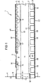
- the thyristor shown in cross section in FIG. 1 has a rotationally symmetrical structure with respect to the axis 4 that is perpendicular to the two main surfaces 2/3 of the semiconductor body 1.
- the disk-shaped semiconductor body 1 made of silicon has a plurality of differently doped and each through pn junctions 9- 11 separate areas 5-8 with the dopant profiles shown in FIG. These areas of different conductivity form the n + emitter 5 contacted by the cathode 12, the p-base 6 on the cathode side, the only weakly electron-conducting n-base 7 provided with an n + stop zone 7 ′ (buffer layer) and the n-base 7 Anode 13 contacted p + emitter 8 of the thyristor.
- the p + emitter 8 is advantageously equipped with anode short circuits 19.
- the structure 15/16 arranged between the gate electrode 14 and the cathode 12 is usually referred to as an “amplifying gate”. It consists of an n + -doped region 15 (auxiliary emitter) embedded in the cathode-side base 6 and a metallization 16 contacting both the n + -doped region 15 and the p-base 6.
- this structure 15/16 forms an auxiliary or pilot thyristor serving as a driver stage for the main thyristor, which considerably amplifies the control current fed into the p-base 6 via the gate electrode 14.
- the emitter short-circuits 17 present in the area of the cathode 12 ensure that the thyristor does not ignite uncontrolled even when the static breakdown voltage is reached, even with a large dU / dt load of a few 1000 V / ⁇ s.
- the overhead ignition of the thyristor according to the invention is not forced by an avalanche, but by the so-called "punch through” effect.
- the "punch through” is the extension of the space charge zone of the p-base / n-base junction 10, which is polarized in the reverse direction, to the adjacent n-base / p-emitter junction 11, which is poled in the forward direction, and from it to understand the resulting steep increase in the leakage current within the semiconductor structure comprising the two pn junctions 10/11.
- the breakdown voltage in the range of the operating temperatures (5 ° C.-120 ° C.) no longer changes or only insignificant.
- the dopant concentration of the n + stop zone 7 'in the area 18 below the gate electrode 14 (radius R ⁇ 1-3 mm) is opposite laterally adjacent and extending to the edge of the pane of the stop zone 7 'significantly reduced.
- the comparatively weak doping in the central region 18 of the stop zone 7 ' causes the space charge zone assigned to the pn junction 10 to expand up to the p + emitter 8 when a high breakover voltage is applied, the reverse current consequently increases sharply and the central thyristor region into the conductive state passes.
- the space charge zone cannot reach the n-base / p-emitter junction 11 due to the higher doping of the n + stop zone 7 ', which prevents a current rise caused by punch through.
- the doping of the n + stop zone 7 'outside the central region 18 can be used to influence the transistor gain ⁇ pnp and thus also the level of the blocking voltage and the forward voltage of the thyristor for a given dopant concentration in the p + emitter 8 (see PESC 88 Record (April 1988), pp. 934-939 (Mitlehner et al.)).
- the phosphorus implantation dose that determines the dopant concentration can only be varied within a relatively narrow range in order to ensure the required high blocking voltage ( ⁇ pnp as small as possible) with a low forward voltage ( ⁇ pnp as large as possible).
- the above statements relate to a gate-controlled thyristor.
- the temperature dependence can also be reduced the breakdown voltage of an ignitable asymmetrical Significantly reduce thyristors by using the below the radiation-sensitive thyristor structure the stop zone is weakly doped than the laterally adjacent one Area.
Landscapes
- Thyristors (AREA)
Description
- ganzflächige, anodenseitige Implantation von Phosphorionen mit einer Dosis von beispielsweise 0,3 - 2 • 1012 cm-2, welche "punch through" ermöglicht;
- Aufbringen einer als Implantationsmaske dienenden Fotolackoder SiO2-Schicht der Dicke d = 1 µm im Zentralbereich des Halbleiterkörpers 1;
- anodenseitige maskierte Implantation von Phosphorionen mit einer Dosis von beispielsweise 3 - 10 • 1014 cm-2, welche "punch through" verhindert;
- Ablösen der Fotolack- oder SiO2-Schicht und
- Eindiffundieren der Phosphoratome bei hoher Temperatur (T ≈ 1240 °C) innerhalb einer Zeitspanne von etwa 10-30 Stunden.
Claims (5)
- Asymmetrischer Thyristor mit dem folgenden Aufbau:dieser Thyristor ista) Er besitzt einen mit einer als Kathode dienenden ersten Elektrode (12) und einer als Anode dienenden zweiten Elektrode (13) versehenen Halbleiterkörper (1), wobei der Halbleiterkörper (1) mehrere unterschiedlich dotierte Bereiche (5-8) aufweist;b) die Dotierung und Lage der Bereiche (5-8) sind derart vorgegeben, daß die Bereiche einen kathodenseitigen Emitter (5) eines ersten Leitungstyps, eine kathodenseitige Basis (6) eines zweiten Leitungstyps, eine anodenseitige Basis (7) des ersten Leitungstyps und einen anodenseitigen Emitter (8) des zweiten Leitungstyps bilden;c) in der anodenseitigen Basis (7) befindet sich eine Stoppzone (7') des ersten Leitungstyps;
dadurch gekennzeichnet, d a ß
die Stoppzone (7') einen unterhalb eines Zündkontaktes (14) oder einer lichtempfindlichen Struktur liegenden Zentralbereich (18) und einen lateral daran angrenzenden Bereich aufweist,
die Stoppzone (7') in dem Zentralbereich schwächer dotiert ist als im lateral angrenzenden Bereich und
der anodenseitige Emitter (8) mit Anodenkurzschlüssen (19) versehen ist. - Asymmetrischer Thyristor nach Anspruch 1,
dadurch gekennzeichnet, daß die Dotierung des zentralen Bereichs (18) und des lateral angrenzenden Bereichs der Stoppzone (7') derart gewählt sind, daß die Raumladungszone des die kathodenseitige und die anodenseitige Basis (6/7) trennenden pn-Übergangs (10) den anodenseitigen pn-Übergang (11) bei einem vorgegebenen Wert der Differenz des Kathoden- und Anodenpotentials ausschließlich im Zentralbereich des Halbleiterkörpers (1) erreicht. - Asymmetrischer Thyristor nach Anspruch 1 oder 2,
dadurch gekennzeichnet, daß eine auf einer kathodenseitigen Hauptfläche (2) des Halbleiterkörpers (1) angeordnete Metallisierung (16) sowohl die kathodenseitige Basis (6) als auch einen in die kathodenseitige Basis (6) eingebetteten Hilfsemitter (15) des ersten Leitungstyps kontaktiert. - Asymmetrischer Thyristor nach einem der Ansprüche 1 bis 3,
dadurch gekennzeichnet, daß die Stoppzone (7') eine lateral inhomogene Verteilung aufweist, die durch Implantation eines Dotierstoffes erzeugt wird, wobei die Dosis des Dotierstoffes im zentralen Bereich der Stoppzone (7') um einen Faktor 100-5000 niedriger ist als im lateral angrenzenden Bereich. - Asymmetrischer Thyristor nach Anspruch 4,
dadurch gekennzeichnet, daß die Dosis des Dotierstoffes im zentralen Bereich (18) der Stoppzone (7') 0,3 - 2 • 1012 cm-2 beträgt.
Applications Claiming Priority (3)
| Application Number | Priority Date | Filing Date | Title |
|---|---|---|---|
| DE19703673 | 1997-01-31 | ||
| DE19703673 | 1997-01-31 | ||
| PCT/DE1998/000248 WO1998034282A1 (de) | 1997-01-31 | 1998-01-28 | Asymmetrischer thyristor |
Publications (2)
| Publication Number | Publication Date |
|---|---|
| EP0970525A1 EP0970525A1 (de) | 2000-01-12 |
| EP0970525B1 true EP0970525B1 (de) | 2003-05-21 |
Family
ID=7818955
Family Applications (1)
| Application Number | Title | Priority Date | Filing Date |
|---|---|---|---|
| EP98909291A Expired - Lifetime EP0970525B1 (de) | 1997-01-31 | 1998-01-28 | Asymmetrischer thyristor |
Country Status (5)
| Country | Link |
|---|---|
| US (1) | US6271545B1 (de) |
| EP (1) | EP0970525B1 (de) |
| JP (1) | JP2001508945A (de) |
| DE (1) | DE59808468D1 (de) |
| WO (1) | WO1998034282A1 (de) |
Families Citing this family (9)
| Publication number | Priority date | Publication date | Assignee | Title |
|---|---|---|---|---|
| DE50015361D1 (de) * | 1999-02-22 | 2008-10-30 | Infineon Technologies Ag | Verfahren zum einstellen der durchbruchspannung eines thyristors |
| DE19947028A1 (de) | 1999-09-30 | 2001-04-12 | Siemens Ag | Thyristor mit Spannungsstoßbelastbarkeit in der Freiwerdezeit |
| DE10016233A1 (de) * | 2000-03-31 | 2001-10-11 | Siemens Ag | Abschaltbarer Thyristor |
| US6989900B1 (en) * | 2001-04-02 | 2006-01-24 | Advanced Micro Devices, Inc. | Method of measuring implant profiles using scatterometric techniques |
| DE10250575B4 (de) * | 2002-10-30 | 2010-04-15 | Infineon Technologies Ag | IGBT mit monolithisch integrierter antiparalleler Diode |
| DE102004025082B4 (de) * | 2004-05-21 | 2006-12-28 | Infineon Technologies Ag | Elektrisch und durch Strahlung zündbarer Thyristor und Verfahren zu dessen Kontaktierung |
| DE102005023479B4 (de) * | 2005-05-20 | 2011-06-09 | Infineon Technologies Ag | Thyristor mit Zündstufenstruktur |
| JP5011748B2 (ja) * | 2006-02-24 | 2012-08-29 | 株式会社デンソー | 半導体装置 |
| CN100578819C (zh) * | 2008-06-05 | 2010-01-06 | 古捷玉 | 太阳能电池的光伏板及带有该光伏板的集光发电装置 |
Family Cites Families (9)
| Publication number | Priority date | Publication date | Assignee | Title |
|---|---|---|---|---|
| DE2238564C3 (de) * | 1972-08-04 | 1981-02-19 | Siemens Ag, 1000 Berlin Und 8000 Muenchen | Thyristor |
| DE3369234D1 (en) * | 1982-11-15 | 1987-02-19 | Toshiba Kk | Thyristor device protected from an overvoltage |
| JPS60115263A (ja) * | 1983-11-28 | 1985-06-21 | Toshiba Corp | 半導体装置 |
| GB2150753B (en) * | 1983-11-30 | 1987-04-01 | Toshiba Kk | Semiconductor device |
| EP0144876B1 (de) * | 1983-12-07 | 1988-03-09 | BBC Brown Boveri AG | Halbleiterbauelement |
| JPS61202465A (ja) | 1985-03-06 | 1986-09-08 | Toshiba Corp | 過電圧保護機能付サイリスタ |
| US5049965A (en) * | 1987-11-20 | 1991-09-17 | Siemens Aktiengesellschaft | Thyristor having adjustable breakover voltage and method of manufacture |
| US5352910A (en) * | 1992-04-07 | 1994-10-04 | Tokyo Denki Seizo Kabushiki Kaisha | Semiconductor device with a buffer structure |
| DE4420252A1 (de) * | 1994-06-10 | 1995-12-14 | Abb Management Ag | Anodenseitige Shortstruktur für asymmetrische Thyristoren |
-
1998
- 1998-01-28 DE DE59808468T patent/DE59808468D1/de not_active Expired - Lifetime
- 1998-01-28 JP JP53244698A patent/JP2001508945A/ja active Pending
- 1998-01-28 EP EP98909291A patent/EP0970525B1/de not_active Expired - Lifetime
- 1998-01-28 WO PCT/DE1998/000248 patent/WO1998034282A1/de not_active Ceased
- 1998-01-28 US US09/355,061 patent/US6271545B1/en not_active Expired - Lifetime
Also Published As
| Publication number | Publication date |
|---|---|
| EP0970525A1 (de) | 2000-01-12 |
| JP2001508945A (ja) | 2001-07-03 |
| US6271545B1 (en) | 2001-08-07 |
| WO1998034282A1 (de) | 1998-08-06 |
| DE59808468D1 (en) | 2003-06-26 |
Similar Documents
| Publication | Publication Date | Title |
|---|---|---|
| DE69232461T2 (de) | Verfahren zum herstellen von transistoren mit isoliertem gate unter verwendung von platin zur kontrolle der lebensdauer | |
| EP0200863B1 (de) | Halbleiterbauelement mit Thyristor- und Diodenstrukturen | |
| DE3689680T2 (de) | Mittels Steuerelektrode abschaltbarer Thyristor mit unabhängigen Zünd-/Lösch-Kontrolltransistoren. | |
| DE69319549T2 (de) | Spannungsgesteuerte Halbleiteranordnung | |
| DE102016112721B4 (de) | n-Kanal-Leistungshalbleitervorrichtung mit p-Schicht im Driftvolumen | |
| DE102019214213A1 (de) | Halbleitervorrichtung | |
| WO2000042662A1 (de) | Leistungshalbleiterbauelement mit mesa-randabschluss | |
| DE102007030804A1 (de) | Halbleitervorrichtung | |
| DE112021002169T5 (de) | Halbleitervorrichtung | |
| DE102020204455B4 (de) | Halbleitervorrichtung | |
| EP0970525B1 (de) | Asymmetrischer thyristor | |
| DE102022102521A1 (de) | Halbleitervorrichtung und Verfahren zum Herstellen derselben | |
| DE19528998C2 (de) | Bidirektionaler Halbleiterschalter und Verfahren zu seiner Steuerung | |
| EP0564007B1 (de) | Thyristor mit reduzierter Kippspannung | |
| DE4121375A1 (de) | Abschaltbares leistungshalbleiter-bauelement sowie verfahren zu dessen herstellung | |
| DE3328231C2 (de) | ||
| EP0062099B1 (de) | Thyristor und Verfahren zu seinem Betrieb | |
| DE10117483A1 (de) | Halbleiterleistungsbauelement und entsprechendes Herstellungsverfahren | |
| DE19650762A1 (de) | Thyristor mit Durchbruchbereich | |
| EP1216488B1 (de) | Thyristor mit spannungsstossbelastbarkeit in der freiwerdezeit | |
| EP0902979B1 (de) | Thyristor mit integriertem du/dt-schutz | |
| EP0017980B1 (de) | Thyristor mit Steuerung durch Feldeffekttransistor | |
| EP0062100B1 (de) | Thyristor mit innerer Stromverstärkung und Verfahren zu seinem Betrieb | |
| EP0062102B1 (de) | Thyristor mit anschaltbarer innerer Stromverstärkung und Verfahren zu seinem Betrieb | |
| EP0666601A2 (de) | Abschaltbares Halbleiterbauelement |
Legal Events
| Date | Code | Title | Description |
|---|---|---|---|
| PUAI | Public reference made under article 153(3) epc to a published international application that has entered the european phase |
Free format text: ORIGINAL CODE: 0009012 |
|
| 17P | Request for examination filed |
Effective date: 19990720 |
|
| AK | Designated contracting states |
Kind code of ref document: A1 Designated state(s): CH DE FR GB LI |
|
| RAP1 | Party data changed (applicant data changed or rights of an application transferred) |
Owner name: INFINEON TECHNOLOGIES AG |
|
| 17Q | First examination report despatched |
Effective date: 20010511 |
|
| GRAH | Despatch of communication of intention to grant a patent |
Free format text: ORIGINAL CODE: EPIDOS IGRA |
|
| GRAH | Despatch of communication of intention to grant a patent |
Free format text: ORIGINAL CODE: EPIDOS IGRA |
|
| GRAA | (expected) grant |
Free format text: ORIGINAL CODE: 0009210 |
|
| AK | Designated contracting states |
Designated state(s): CH DE FR GB LI |
|
| REG | Reference to a national code |
Ref country code: GB Ref legal event code: FG4D Free format text: NOT ENGLISH |
|
| REG | Reference to a national code |
Ref country code: CH Ref legal event code: EP |
|
| REF | Corresponds to: |
Ref document number: 59808468 Country of ref document: DE Date of ref document: 20030626 Kind code of ref document: P |
|
| REG | Reference to a national code |
Ref country code: CH Ref legal event code: NV Representative=s name: INFINEON TECHNOLOGIES SCHWEIZ AG |
|
| GBT | Gb: translation of ep patent filed (gb section 77(6)(a)/1977) | ||
| ET | Fr: translation filed | ||
| PLBE | No opposition filed within time limit |
Free format text: ORIGINAL CODE: 0009261 |
|
| STAA | Information on the status of an ep patent application or granted ep patent |
Free format text: STATUS: NO OPPOSITION FILED WITHIN TIME LIMIT |
|
| 26N | No opposition filed |
Effective date: 20040224 |
|
| PGFP | Annual fee paid to national office [announced via postgrant information from national office to epo] |
Ref country code: CH Payment date: 20090115 Year of fee payment: 12 |
|
| REG | Reference to a national code |
Ref country code: CH Ref legal event code: PFA Owner name: INFINEON TECHNOLOGIES AG Free format text: INFINEON TECHNOLOGIES AG#ST.-MARTIN-STRASSE 53#81669 MUENCHEN (DE) -TRANSFER TO- INFINEON TECHNOLOGIES AG#ST.-MARTIN-STRASSE 53#81669 MUENCHEN (DE) |
|
| PGFP | Annual fee paid to national office [announced via postgrant information from national office to epo] |
Ref country code: FR Payment date: 20090115 Year of fee payment: 12 |
|
| REG | Reference to a national code |
Ref country code: CH Ref legal event code: PL |
|
| REG | Reference to a national code |
Ref country code: FR Ref legal event code: ST Effective date: 20100930 |
|
| PG25 | Lapsed in a contracting state [announced via postgrant information from national office to epo] |
Ref country code: LI Free format text: LAPSE BECAUSE OF NON-PAYMENT OF DUE FEES Effective date: 20100131 Ref country code: FR Free format text: LAPSE BECAUSE OF NON-PAYMENT OF DUE FEES Effective date: 20100201 Ref country code: CH Free format text: LAPSE BECAUSE OF NON-PAYMENT OF DUE FEES Effective date: 20100131 |
|
| PGFP | Annual fee paid to national office [announced via postgrant information from national office to epo] |
Ref country code: DE Payment date: 20170125 Year of fee payment: 20 |
|
| PGFP | Annual fee paid to national office [announced via postgrant information from national office to epo] |
Ref country code: GB Payment date: 20170125 Year of fee payment: 20 |
|
| REG | Reference to a national code |
Ref country code: DE Ref legal event code: R071 Ref document number: 59808468 Country of ref document: DE |
|
| REG | Reference to a national code |
Ref country code: GB Ref legal event code: PE20 Expiry date: 20180127 |
|
| PG25 | Lapsed in a contracting state [announced via postgrant information from national office to epo] |
Ref country code: GB Free format text: LAPSE BECAUSE OF EXPIRATION OF PROTECTION Effective date: 20180127 |