EP0966035B1 - Procédé de métallisation pour semiconducteur - Google Patents
Procédé de métallisation pour semiconducteur Download PDFInfo
- Publication number
- EP0966035B1 EP0966035B1 EP99110469A EP99110469A EP0966035B1 EP 0966035 B1 EP0966035 B1 EP 0966035B1 EP 99110469 A EP99110469 A EP 99110469A EP 99110469 A EP99110469 A EP 99110469A EP 0966035 B1 EP0966035 B1 EP 0966035B1
- Authority
- EP
- European Patent Office
- Prior art keywords
- dielectric layer
- conductors
- layer
- metalization
- disposed
- Prior art date
- Legal status (The legal status is an assumption and is not a legal conclusion. Google has not performed a legal analysis and makes no representation as to the accuracy of the status listed.)
- Expired - Lifetime
Links
Images

Classifications
-
- H—ELECTRICITY
- H01—ELECTRIC ELEMENTS
- H01L—SEMICONDUCTOR DEVICES NOT COVERED BY CLASS H10
- H01L21/00—Processes or apparatus adapted for the manufacture or treatment of semiconductor or solid state devices or of parts thereof
- H01L21/02—Manufacture or treatment of semiconductor devices or of parts thereof
- H01L21/04—Manufacture or treatment of semiconductor devices or of parts thereof the devices having potential barriers, e.g. a PN junction, depletion layer or carrier concentration layer
- H01L21/18—Manufacture or treatment of semiconductor devices or of parts thereof the devices having potential barriers, e.g. a PN junction, depletion layer or carrier concentration layer the devices having semiconductor bodies comprising elements of Group IV of the Periodic Table or AIIIBV compounds with or without impurities, e.g. doping materials
- H01L21/28—Manufacture of electrodes on semiconductor bodies using processes or apparatus not provided for in groups H01L21/20 - H01L21/268
-
- H—ELECTRICITY
- H01—ELECTRIC ELEMENTS
- H01L—SEMICONDUCTOR DEVICES NOT COVERED BY CLASS H10
- H01L21/00—Processes or apparatus adapted for the manufacture or treatment of semiconductor or solid state devices or of parts thereof
- H01L21/70—Manufacture or treatment of devices consisting of a plurality of solid state components formed in or on a common substrate or of parts thereof; Manufacture of integrated circuit devices or of parts thereof
- H01L21/71—Manufacture of specific parts of devices defined in group H01L21/70
- H01L21/768—Applying interconnections to be used for carrying current between separate components within a device comprising conductors and dielectrics
- H01L21/76801—Applying interconnections to be used for carrying current between separate components within a device comprising conductors and dielectrics characterised by the formation and the after-treatment of the dielectrics, e.g. smoothing
- H01L21/76802—Applying interconnections to be used for carrying current between separate components within a device comprising conductors and dielectrics characterised by the formation and the after-treatment of the dielectrics, e.g. smoothing by forming openings in dielectrics
- H01L21/76807—Applying interconnections to be used for carrying current between separate components within a device comprising conductors and dielectrics characterised by the formation and the after-treatment of the dielectrics, e.g. smoothing by forming openings in dielectrics for dual damascene structures
-
- H—ELECTRICITY
- H01—ELECTRIC ELEMENTS
- H01L—SEMICONDUCTOR DEVICES NOT COVERED BY CLASS H10
- H01L21/00—Processes or apparatus adapted for the manufacture or treatment of semiconductor or solid state devices or of parts thereof
- H01L21/70—Manufacture or treatment of devices consisting of a plurality of solid state components formed in or on a common substrate or of parts thereof; Manufacture of integrated circuit devices or of parts thereof
- H01L21/71—Manufacture of specific parts of devices defined in group H01L21/70
- H01L21/768—Applying interconnections to be used for carrying current between separate components within a device comprising conductors and dielectrics
- H01L21/76838—Applying interconnections to be used for carrying current between separate components within a device comprising conductors and dielectrics characterised by the formation and the after-treatment of the conductors
- H01L21/76885—By forming conductive members before deposition of protective insulating material, e.g. pillars, studs
-
- H—ELECTRICITY
- H01—ELECTRIC ELEMENTS
- H01L—SEMICONDUCTOR DEVICES NOT COVERED BY CLASS H10
- H01L23/00—Details of semiconductor or other solid state devices
- H01L23/52—Arrangements for conducting electric current within the device in operation from one component to another, i.e. interconnections, e.g. wires, lead frames
- H01L23/522—Arrangements for conducting electric current within the device in operation from one component to another, i.e. interconnections, e.g. wires, lead frames including external interconnections consisting of a multilayer structure of conductive and insulating layers inseparably formed on the semiconductor body
- H01L23/5222—Capacitive arrangements or effects of, or between wiring layers
-
- H—ELECTRICITY
- H01—ELECTRIC ELEMENTS
- H01L—SEMICONDUCTOR DEVICES NOT COVERED BY CLASS H10
- H01L23/00—Details of semiconductor or other solid state devices
- H01L23/52—Arrangements for conducting electric current within the device in operation from one component to another, i.e. interconnections, e.g. wires, lead frames
- H01L23/522—Arrangements for conducting electric current within the device in operation from one component to another, i.e. interconnections, e.g. wires, lead frames including external interconnections consisting of a multilayer structure of conductive and insulating layers inseparably formed on the semiconductor body
- H01L23/528—Layout of the interconnection structure
- H01L23/5283—Cross-sectional geometry
-
- H—ELECTRICITY
- H01—ELECTRIC ELEMENTS
- H01L—SEMICONDUCTOR DEVICES NOT COVERED BY CLASS H10
- H01L2924/00—Indexing scheme for arrangements or methods for connecting or disconnecting semiconductor or solid-state bodies as covered by H01L24/00
- H01L2924/0001—Technical content checked by a classifier
- H01L2924/0002—Not covered by any one of groups H01L24/00, H01L24/00 and H01L2224/00
Definitions
- This invention relates generally to semiconductor metalization system and methods and more particularly to metalization systems having reduced inter-conductor capacitance.
- RIE reactive ion etching
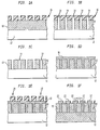
- a dielectric layer 10 is formed over a semiconductor substrate 12, as shown in FIG. 1A.
- Via holes 14 are etched through selected regions of the dielectric layer 10 using a patterned photoresist mask 16, as shown in FIG. 1B.
- the mask 16 is removed as shown in FIG. 1C.
- a metalization layer 18 is deposited over the surface of the etched dielectric layer 12 and through the etched via holes 14, as shown in FIG. 1D.
- a second photoresist layer 20 is then patterned as shown in FIG.
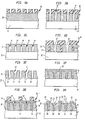
- a dielectric layer 10 is formed over a semiconductor substrate 12, as shown in FIG. 2A.
- Via holes 14 are etched through selected portions of the dielectric layer 10 using a patterned photoresist mask 16, as shown in FIG. 2B.
- the mask 16 is removed, as shown in FIG. 2C.
- a second photoresist layer 16' is formed over the dielectric layer 10 and is patterned to expose surface portions of the dielectric layer 10 disposed around the periphery 15 of the via holes 14, as shown in FIG. 2D.
- the exposed surface portions of the dielectric layer 10 are etched to form recesses 14' in the dielectric layer 10 around the upper portions of the via holes 14, as shown in FIG. 2E.
- a metalization layer 18 is deposited over the surface of the etched dielectric layer 10, portions of the metalization layer passing through the via holes 14, other portions of the metalization layer being disposed in the recesses 14' and still other portions of the metalization layer 18 being disposed on the surface of the dielectric layer 10, as shown in FIG. 2F.
- the portions of the metalization layer 18 disposed on the upper surface of the dielectric layer 10 are removed by, for example, chemical mechanical polishing (CMP) to thereby form the dielectrically isolated conductors, as shown in FIG. 2G. It is noted that the upper surface portions of the conductors 22' are exposed for connection to other devices or other metalization layers, not shown, which may be formed over the metalization layer 18.
- CMP chemical mechanical polishing
- the capacitance between adjacent conductors 22, 22' is inversely proportional to the distance, d, between such adjacent conductors.
- d the distance between such adjacent conductors.
- WO 97/47036 A discloses a multilevel interconnect structure comprising several levels of conductors. Conductors of one level are staggered with respect to conductors on another level.
- a method for forming a metalization system includes providing a substrate.
- a dielectric layer is formed over a surface of the substrate.
- a plurality of via holes is formed into a surface of the dielectric layer, such holes passing through the dielectric layer.
- Recesses are formed in the surface of the dielectric layer, such recesses terminating in a portion of the plurality of via holes passing through the dielectric layer.
- a metalization layer is deposited over the surface of the dielectric layer, portions of the metalization layer passing through the via holes, portions of the metalization layer being disposed in the recesses and portions of the metalization layer being disposed on the surface of the dielectric layer.
- the metalization layer is patterned into a plurality of conductors, one portion of the conductors being disposed on the surface the dielectric layer and another portion of the conductors disposed in the recesses.
- electrical conductors are formed on different level using one only masking-etching step to form the via holes through the dielectric layer and only one metalization deposition step to deposit the metalization layer which provides both levels of conductors.
- one of the conductors on the surface is formed adjacent to one of the conductors recessed into a portion of the surface of the dielectric layer.
- the plurality of conductors are formed parallel to one another.
- the first-mentioned portion of the plurality of conductors have lower surface portions thereof formed on an upper surface of the dielectric layer and wherein the conductors recessed into a portion of the surface of the dielectric layer have upper surface portions thereof formed along the upper surface of the dielectric layer.
- a substrate 12 here for example a semiconductor substrate, is provided having formed therein a plurality of active devices, not shown.
- a dielectric layer 10 is formed over a surface of the substrate 12.
- a plurality of via holes 14 is formed through the dielectric layer 10, as shown in FIG. 3C, using etching mask 16 as shown in FIG. 3B and any conventional photolithographic-etching technique.
- the holes 14 are etched through the dielectric layer 10 to the substrate 12.
- a second mask 16" is formed over the structure, as shown in FIG. 3D. It is noted that the mask 16" is similar to the mask 16' in FIG. 2D. Here, however, the opening in the mask 16" are over only certain ones of the holes 14.
- Recesses 14' are formed in the upper portions of the upper surface of the dielectric layer 10 exposed by the openings in the mask 16", as shown in FIG. 3E.
- the recesses 14' terminate in an upper portion of the plurality of via holes 14 passing through the dielectric layer 10.
- a metalization layer 18 is deposited over the upper surface of the dielectric layer 10, as shown in FIG. 3F. Portions of the metalization layer 18 pass through the via holes 14, other portions of the metalization layer 18 are disposed in the recesses 14', and still other portions of the metalization layer 18 are disposed on the upper surface of the dielectric layer 10, as shown in FIG. 3F.
- the metalization layer 18 is masked with a mask 16'", as shown in FIG. 3G.
- the metalization layer 18 is patterned into a plurality of conductors 22, 22' with a mask 16'" using a RIE process to produce the structure shown in FIG. 3H.
- One portion of the conductors 22 are disposed on the surface of the dielectric layer 10 and another portion of the conductors 22' are disposed in the recesses 14', as shown in FIG. 3H.
- the dielectric layer 10 formed over a semiconductor substrate 12 is silicon dioxide, being understood that other dielectric materials may also be used.
- the via holes 14 are etched through the dielectric layer 10 using a patterned photoresist mask, as shown in FIG. 3B. The holes are etch with a pitch desired for separation between electrical conductors being formed.
- the second photoresist layer 16" is formed over the dielectric layer 10 and patterned to expose surface portions of the dielectric layer 10 disposed around certain ones of the via holes 14, as shown in FIG. 3D. It is noted that apertures are formed in the mask 16" over alternating one of the vis holes 14.
- the exposed surface portions of the dielectric layer 10 are etched to form recesses 14' in the dielectric layer 10 around the via holes, as shown in FIG. 3E. It is noted that the recesses 14' are formed in the upper portions of only alternating ones of the via holes 14.
- the metalization layer 18 (FIG. 3F) is deposited over the surface of the etched dielectric layer 10, portions of the metalization layer 18 passing through the via holes 14, other portions of the metalization layer 18 being disposed in the recesses 14' and still other portions of the metalization layer 18 being disposed on the surface of the dielectric layer 10, as shown in FIG. 3G.
- a third photoresist layer 16'" is disposed over the metalization layer 18, as shown in FIG. 3G. It is noted that apertures in the mask 16'" are disposed over only the recesses 14' with such mask 16'" being disposed over the via holes 14 which do not have the recesses 14'.
- the mask 16'" is used as an etching mask to pattern the metalization layer 18 as shown in FIG. 3H.
- the metalization layer 18 (FIG. 3G) is patterned into electrical conductors 22, 22'. More particularly, a RIE process is used to remove the exposed portions of the metalization layer 18 to thereby form the dielectrically isolated conductors, 22, 22' as shown in FIG. 3H.
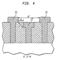
- a metalization system for an integrated circuit wherein the semiconductor substrate 12 has the dielectric layer 10 disposed over it.
- the plurality of electrical conductors 22, 22' is provided, one portion of the conductors, i.e., portion 22, being disposed on the surface of the dielectric layer, here the upper surface of the dielectric layer 10, and another portion of the conductors 22' being recessed in a surface portion of the dielectric layer 10.
- the conductors 22 are adjacent to the conductors 22' recessed into a portion of the surface of the dielectric layer 10.
- Each one of the plurality of conductors 22, 22' has a portion 30 thereof extending through the dielectric layer 10.
- the plurality of conductors 22, 22' run parallel to one another in a direction perpendicular to the plane of the paper.
- the plurality of conductors 22 have lower surface portions 32 thereof disposed on an upper surface 33 of the dielectric layer 10 and the conductors 22' recessed into a portion of the surface of the dielectric layer 10 have upper surface portions 34 thereof disposed along the upper surface 33 of the dielectric layer 10.
- the distance between adjacent conductors 22, 22' is increased in comparison with the distance d between the sidewalls of adjacent conductors 22' described above in connection with FIG. 2G. For example, referring to FIG.
- the distance d is the pitch between adjacent conductors 22'; advantageously, the actual distance d' separating the current carrying portions of the adjacent conductors 22, 22' is greater than the pitch d. Further, the distance d" between adjacent conductors on the same plane, e.g., conductors 22, conductors 22', respectively is greater than the pitch d.
- the process described above may be used with many different conductive materials, such a doped amorphous or polycrystalline silicon, or metals including one, or a combination of, the following: titanium, titanium nitride, tungsten nitride, aluminum, cobalt, tantalum, tantalum nitride, copper, silver, gold, platinum, rubidium, rubidium oxide, iridium or iridium oxide, for example.
- the patterning of the metalization layer may be by etching such metalization layer using reactive ion etching, ion milling, anisotropic dry etching, or wet etching when the pitch is relatively large, for example.
- the conductors may be used for word lines, bit lines, address lines and control clock lines in DRAM cells, for example, and for data bus lines and input/output lines in most semiconductor devices, for example.
- the substrate 12 above is a semiconductor substrate
- the substrate may be a metalization layer.
Landscapes
- Engineering & Computer Science (AREA)
- Physics & Mathematics (AREA)
- Condensed Matter Physics & Semiconductors (AREA)
- General Physics & Mathematics (AREA)
- Computer Hardware Design (AREA)
- Microelectronics & Electronic Packaging (AREA)
- Power Engineering (AREA)
- Manufacturing & Machinery (AREA)
- Geometry (AREA)
- Internal Circuitry In Semiconductor Integrated Circuit Devices (AREA)
- Electrodes Of Semiconductors (AREA)
Claims (6)
- Procédé de formation d'un système de métallisation, consistant à :prévoir un support (12),former une couche diélectrique (10) sur une surface du support (12),former une pluralité de trous d'interconnexion (14) dans la surface de la couche diélectrique (10), ces trous d'interconnexion (14) traversant la couche diélectrique (10) jusqu'au support (12),former des évidements (14') dans la surface de la couche diélectrique (10), ces évidements se terminant dans certains des trous d'interconnexion (14) traversant la couche diélectrique,déposer une couche de métallisation (18) à la surface de la couche diélectrique (10), des parties de la couche de métallisation (18) étant disposées à travers les trous d'interconnexion (14), des parties étant disposées dans les évidements (14') et des parties étant disposées à la surface de la couche diélectrique (10),configurer la couche de métallisation en une pluralité de conducteurs (22, 22') de sorte que certains (22) des conducteurs sont disposés à la surface de la couche diélectrique (10) et les autres (22') sont disposés dans les évidements (14'), et de sorte que chaque conducteur (22, 22') est en contact direct avec une partie respective de la couche de métallisation disposée dans un trou d'interconnexion.
- Procédé selon la revendication 1,
caractérisé en ce que
le support (12) est un support semi-conducteur. - Procédé selon la revendication 1,
caractérisé en ce que
le support (12) est une couche de métallisation. - Procédé selon la revendication 1,
caractérisé en ce que
les conducteurs (22, 22') sont parallèles les uns aux autres. - Procédé selon la revendication 1,
caractérisé en ce que
les conducteurs (22') disposés dans les évidements (14') ont des parties de leur surface supérieure disposées le long de la surface de la couche diélectrique (10). - Procédé selon la revendication 1,
caractérisé en ce que
les conducteurs (22) disposés à la surface de la couche diélectrique (10) et les conducteurs (22') disposés dans les évidements (14') sont formés de manière alternée.
Applications Claiming Priority (2)
| Application Number | Priority Date | Filing Date | Title |
|---|---|---|---|
| US99093 | 1998-06-17 | ||
| US09/099,093 US6137178A (en) | 1998-06-17 | 1998-06-17 | Semiconductor metalization system and method |
Publications (2)
| Publication Number | Publication Date |
|---|---|
| EP0966035A1 EP0966035A1 (fr) | 1999-12-22 |
| EP0966035B1 true EP0966035B1 (fr) | 2006-03-01 |
Family
ID=22272661
Family Applications (1)
| Application Number | Title | Priority Date | Filing Date |
|---|---|---|---|
| EP99110469A Expired - Lifetime EP0966035B1 (fr) | 1998-06-17 | 1999-05-31 | Procédé de métallisation pour semiconducteur |
Country Status (7)
| Country | Link |
|---|---|
| US (1) | US6137178A (fr) |
| EP (1) | EP0966035B1 (fr) |
| JP (1) | JP2000031280A (fr) |
| KR (1) | KR100598256B1 (fr) |
| CN (1) | CN1139112C (fr) |
| DE (1) | DE69930027T2 (fr) |
| TW (1) | TW417204B (fr) |
Families Citing this family (13)
| Publication number | Priority date | Publication date | Assignee | Title |
|---|---|---|---|---|
| FR2786609B1 (fr) * | 1998-11-26 | 2003-10-17 | St Microelectronics Sa | Circuit integre a capacite interlignes reduite et procede de fabrication associe |
| US6849923B2 (en) | 1999-03-12 | 2005-02-01 | Kabushiki Kaisha Toshiba | Semiconductor device and manufacturing method of the same |
| US20060017162A1 (en) * | 1999-03-12 | 2006-01-26 | Shoji Seta | Semiconductor device and manufacturing method of the same |
| US6420252B1 (en) * | 2000-05-10 | 2002-07-16 | Emcore Corporation | Methods of forming robust metal contacts on compound semiconductors |
| US7892962B2 (en) * | 2007-09-05 | 2011-02-22 | Taiwan Semiconductor Manufacturing Company, Ltd. | Nail-shaped pillar for wafer-level chip-scale packaging |
| KR101654820B1 (ko) | 2008-07-09 | 2016-09-06 | 인벤사스 코포레이션 | 감소된 도전체 공간을 가진 마이크로전자 상호접속 소자, 및 그것을 형성하는 방법 |
| US8309446B2 (en) | 2008-07-16 | 2012-11-13 | Applied Materials, Inc. | Hybrid heterojunction solar cell fabrication using a doping layer mask |
| EP2359410A4 (fr) | 2008-12-10 | 2014-09-24 | Applied Materials Inc | Système de visualisation amélioré pour calage de motif de sérigraphie |
| US9064968B2 (en) * | 2013-08-19 | 2015-06-23 | Phison Electronics Corp. | Non-volatile memory device and operation and fabricating methods thereof |
| US8772951B1 (en) | 2013-08-29 | 2014-07-08 | Qualcomm Incorporated | Ultra fine pitch and spacing interconnects for substrate |
| US9159670B2 (en) | 2013-08-29 | 2015-10-13 | Qualcomm Incorporated | Ultra fine pitch and spacing interconnects for substrate |
| KR102377372B1 (ko) * | 2014-04-02 | 2022-03-21 | 어플라이드 머티어리얼스, 인코포레이티드 | 인터커넥트들을 형성하기 위한 방법 |
| US20190067178A1 (en) * | 2017-08-30 | 2019-02-28 | Qualcomm Incorporated | Fine pitch and spacing interconnects with reserve interconnect portion |
Family Cites Families (7)
| Publication number | Priority date | Publication date | Assignee | Title |
|---|---|---|---|---|
| JP3057975B2 (ja) * | 1993-09-27 | 2000-07-04 | 日本電気株式会社 | 集積回路の配線 |
| US5471093A (en) * | 1994-10-28 | 1995-11-28 | Advanced Micro Devices, Inc. | Pseudo-low dielectric constant technology |
| JPH08293523A (ja) * | 1995-02-21 | 1996-11-05 | Seiko Epson Corp | 半導体装置およびその製造方法 |
| US5702982A (en) * | 1996-03-28 | 1997-12-30 | Taiwan Semiconductor Manufacturing Company, Ltd. | Method for making metal contacts and interconnections concurrently on semiconductor integrated circuits |
| US5846876A (en) * | 1996-06-05 | 1998-12-08 | Advanced Micro Devices, Inc. | Integrated circuit which uses a damascene process for producing staggered interconnect lines |
| US5753976A (en) * | 1996-06-14 | 1998-05-19 | Minnesota Mining And Manufacturing Company | Multi-layer circuit having a via matrix interlayer connection |
| KR100219508B1 (ko) * | 1996-12-30 | 1999-09-01 | 윤종용 | 반도체장치의 금속배선층 형성방법 |
-
1998
- 1998-06-17 US US09/099,093 patent/US6137178A/en not_active Expired - Lifetime
-
1999
- 1999-05-31 DE DE69930027T patent/DE69930027T2/de not_active Expired - Lifetime
- 1999-05-31 EP EP99110469A patent/EP0966035B1/fr not_active Expired - Lifetime
- 1999-06-08 TW TW088109515A patent/TW417204B/zh not_active IP Right Cessation
- 1999-06-17 KR KR1019990022670A patent/KR100598256B1/ko not_active Expired - Fee Related
- 1999-06-17 CN CNB991086899A patent/CN1139112C/zh not_active Expired - Fee Related
- 1999-06-17 JP JP11171020A patent/JP2000031280A/ja not_active Withdrawn
Also Published As
| Publication number | Publication date |
|---|---|
| EP0966035A1 (fr) | 1999-12-22 |
| KR100598256B1 (ko) | 2006-07-07 |
| DE69930027D1 (de) | 2006-04-27 |
| DE69930027T2 (de) | 2006-09-14 |
| CN1254949A (zh) | 2000-05-31 |
| US6137178A (en) | 2000-10-24 |
| KR20000006238A (ko) | 2000-01-25 |
| CN1139112C (zh) | 2004-02-18 |
| JP2000031280A (ja) | 2000-01-28 |
| TW417204B (en) | 2001-01-01 |
Similar Documents
| Publication | Publication Date | Title |
|---|---|---|
| US5614765A (en) | Self aligned via dual damascene | |
| US5818110A (en) | Integrated circuit chip wiring structure with crossover capability and method of manufacturing the same | |
| US5300456A (en) | Metal-to-metal antifuse structure | |
| US6081021A (en) | Conductor-insulator-conductor structure | |
| US5055423A (en) | Planarized selective tungsten metallization system | |
| US8786087B2 (en) | Semiconductor device having damascene interconnection structure that prevents void formation between interconnections having transparent dielectric substrate | |
| US6251790B1 (en) | Method for fabricating contacts in a semiconductor device | |
| EP0966035B1 (fr) | Procédé de métallisation pour semiconducteur | |
| EP0329969B1 (fr) | Procédé pour aligner et former des piliers | |
| WO1997022144A1 (fr) | Structures vias a damasquinage inverse | |
| US4808552A (en) | Process for making vertically-oriented interconnections for VLSI devices | |
| WO2020210064A1 (fr) | Puce à semi-conducteur avec lignes conductrices empilées et entrefers | |
| US6495877B1 (en) | Metal capacitors with damascene structures and method for forming the same | |
| US6919265B2 (en) | Semiconductor device with elongated interconnecting member and fabrication method thereof | |
| EP0248668A2 (fr) | Procédé pour la fabrication de circuits métalliques intégrés à multicouche et structures ainsi fabriquées | |
| US6207576B1 (en) | Self-aligned dual damascene arrangement for metal interconnection with low k dielectric constant materials and oxide etch stop layer | |
| US20050140010A1 (en) | Method and structure of manufacturing high capacitance metal on insulator capacitors in copper | |
| EP0827195A1 (fr) | Améliorations relatives aux composants semi-conducteurs | |
| US6359329B1 (en) | Embedded wiring structure and method for forming the same | |
| US6974770B2 (en) | Self-aligned mask to reduce cell layout area | |
| US20040121584A1 (en) | Method of manufacturing a semiconductor device | |
| US5792704A (en) | Method for fabricating wiring in semiconductor device | |
| JP2007534178A (ja) | 低減された層内静電容量を有する集積回路の配線構造 | |
| US6504205B1 (en) | Metal capacitors with damascene structures | |
| EP0234407A1 (fr) | Procédé pour remplir des trous de liaison ou de contact dans une structure de métallisation de VLSI à niveaux multiples |
Legal Events
| Date | Code | Title | Description |
|---|---|---|---|
| PUAI | Public reference made under article 153(3) epc to a published international application that has entered the european phase |
Free format text: ORIGINAL CODE: 0009012 |
|
| AK | Designated contracting states |
Kind code of ref document: A1 Designated state(s): DE FR GB IE IT NL |
|
| AX | Request for extension of the european patent |
Free format text: AL;LT;LV;MK;RO;SI |
|
| 17P | Request for examination filed |
Effective date: 20000324 |
|
| AKX | Designation fees paid |
Free format text: DE FR GB IE IT NL |
|
| RAP1 | Party data changed (applicant data changed or rights of an application transferred) |
Owner name: SIEMENS AKTIENGESELLSCHAFT |
|
| RAP1 | Party data changed (applicant data changed or rights of an application transferred) |
Owner name: INFINEON TECHNOLOGIES AG |
|
| 17Q | First examination report despatched |
Effective date: 20040405 |
|
| RTI1 | Title (correction) |
Free format text: SEMICONDUCTOR METALLIZATION METHOD |
|
| GRAP | Despatch of communication of intention to grant a patent |
Free format text: ORIGINAL CODE: EPIDOSNIGR1 |
|
| GRAS | Grant fee paid |
Free format text: ORIGINAL CODE: EPIDOSNIGR3 |
|
| GRAA | (expected) grant |
Free format text: ORIGINAL CODE: 0009210 |
|
| AK | Designated contracting states |
Kind code of ref document: B1 Designated state(s): DE FR GB IE IT NL |
|
| REG | Reference to a national code |
Ref country code: GB Ref legal event code: FG4D |
|
| REG | Reference to a national code |
Ref country code: IE Ref legal event code: FG4D |
|
| REF | Corresponds to: |
Ref document number: 69930027 Country of ref document: DE Date of ref document: 20060427 Kind code of ref document: P |
|
| PGFP | Annual fee paid to national office [announced via postgrant information from national office to epo] |
Ref country code: NL Payment date: 20060515 Year of fee payment: 8 |
|
| PGFP | Annual fee paid to national office [announced via postgrant information from national office to epo] |
Ref country code: GB Payment date: 20060522 Year of fee payment: 8 |
|
| ET | Fr: translation filed | ||
| PLBE | No opposition filed within time limit |
Free format text: ORIGINAL CODE: 0009261 |
|
| STAA | Information on the status of an ep patent application or granted ep patent |
Free format text: STATUS: NO OPPOSITION FILED WITHIN TIME LIMIT |
|
| REG | Reference to a national code |
Ref country code: HK Ref legal event code: WD Ref document number: 1022047 Country of ref document: HK |
|
| 26N | No opposition filed |
Effective date: 20061204 |
|
| GBPC | Gb: european patent ceased through non-payment of renewal fee |
Effective date: 20070531 |
|
| PG25 | Lapsed in a contracting state [announced via postgrant information from national office to epo] |
Ref country code: NL Free format text: LAPSE BECAUSE OF NON-PAYMENT OF DUE FEES Effective date: 20071201 |
|
| NLV4 | Nl: lapsed or anulled due to non-payment of the annual fee |
Effective date: 20071201 |
|
| PG25 | Lapsed in a contracting state [announced via postgrant information from national office to epo] |
Ref country code: GB Free format text: LAPSE BECAUSE OF NON-PAYMENT OF DUE FEES Effective date: 20070531 |
|
| PGFP | Annual fee paid to national office [announced via postgrant information from national office to epo] |
Ref country code: IT Payment date: 20080524 Year of fee payment: 10 |
|
| PGFP | Annual fee paid to national office [announced via postgrant information from national office to epo] |
Ref country code: IE Payment date: 20080523 Year of fee payment: 10 |
|
| REG | Reference to a national code |
Ref country code: FR Ref legal event code: ST Effective date: 20100129 |
|
| PG25 | Lapsed in a contracting state [announced via postgrant information from national office to epo] |
Ref country code: IE Free format text: LAPSE BECAUSE OF NON-PAYMENT OF DUE FEES Effective date: 20090531 Ref country code: FR Free format text: LAPSE BECAUSE OF NON-PAYMENT OF DUE FEES Effective date: 20090602 |
|
| PGFP | Annual fee paid to national office [announced via postgrant information from national office to epo] |
Ref country code: FR Payment date: 20080425 Year of fee payment: 10 |
|
| PG25 | Lapsed in a contracting state [announced via postgrant information from national office to epo] |
Ref country code: IT Free format text: LAPSE BECAUSE OF NON-PAYMENT OF DUE FEES Effective date: 20090531 |
|
| PGFP | Annual fee paid to national office [announced via postgrant information from national office to epo] |
Ref country code: DE Payment date: 20140619 Year of fee payment: 16 |
|
| REG | Reference to a national code |
Ref country code: DE Ref legal event code: R081 Ref document number: 69930027 Country of ref document: DE Owner name: POLARIS INNOVATIONS LTD., IE Free format text: FORMER OWNER: QIMONDA AG, 81739 MUENCHEN, DE Ref country code: DE Ref legal event code: R081 Ref document number: 69930027 Country of ref document: DE Owner name: INFINEON TECHNOLOGIES AG, DE Free format text: FORMER OWNER: QIMONDA AG, 81739 MUENCHEN, DE |
|
| REG | Reference to a national code |
Ref country code: DE Ref legal event code: R081 Ref document number: 69930027 Country of ref document: DE Owner name: POLARIS INNOVATIONS LTD., IE Free format text: FORMER OWNER: INFINEON TECHNOLOGIES AG, 85579 NEUBIBERG, DE |
|
| REG | Reference to a national code |
Ref country code: DE Ref legal event code: R119 Ref document number: 69930027 Country of ref document: DE |
|
| PG25 | Lapsed in a contracting state [announced via postgrant information from national office to epo] |
Ref country code: DE Free format text: LAPSE BECAUSE OF NON-PAYMENT OF DUE FEES Effective date: 20151201 |