EP0959486A2 - Verfahren zur Herstellung eines luftdichten Gefässes und eines Bilderzeugungsgerät unter Benutzung dieses Gefässes - Google Patents
Verfahren zur Herstellung eines luftdichten Gefässes und eines Bilderzeugungsgerät unter Benutzung dieses Gefässes Download PDFInfo
- Publication number
- EP0959486A2 EP0959486A2 EP99303818A EP99303818A EP0959486A2 EP 0959486 A2 EP0959486 A2 EP 0959486A2 EP 99303818 A EP99303818 A EP 99303818A EP 99303818 A EP99303818 A EP 99303818A EP 0959486 A2 EP0959486 A2 EP 0959486A2
- Authority
- EP
- European Patent Office
- Prior art keywords
- vessel
- getter
- manufacturing
- airtight
- sealing
- Prior art date
- Legal status (The legal status is an assumption and is not a legal conclusion. Google has not performed a legal analysis and makes no representation as to the accuracy of the status listed.)
- Granted
Links
Images


Classifications
-
- H—ELECTRICITY
- H01—ELECTRIC ELEMENTS
- H01J—ELECTRIC DISCHARGE TUBES OR DISCHARGE LAMPS
- H01J1/00—Details of electrodes, of magnetic control means, of screens, or of the mounting or spacing thereof, common to two or more basic types of discharge tubes or lamps
- H01J1/02—Main electrodes
- H01J1/30—Cold cathodes, e.g. field-emissive cathode
-
- H—ELECTRICITY
- H01—ELECTRIC ELEMENTS
- H01J—ELECTRIC DISCHARGE TUBES OR DISCHARGE LAMPS
- H01J9/00—Apparatus or processes specially adapted for the manufacture, installation, removal, maintenance of electric discharge tubes, discharge lamps, or parts thereof; Recovery of material from discharge tubes or lamps
- H01J9/40—Closing vessels
-
- H—ELECTRICITY
- H01—ELECTRIC ELEMENTS
- H01J—ELECTRIC DISCHARGE TUBES OR DISCHARGE LAMPS
- H01J9/00—Apparatus or processes specially adapted for the manufacture, installation, removal, maintenance of electric discharge tubes, discharge lamps, or parts thereof; Recovery of material from discharge tubes or lamps
- H01J9/24—Manufacture or joining of vessels, leading-in conductors or bases
-
- H—ELECTRICITY
- H01—ELECTRIC ELEMENTS
- H01J—ELECTRIC DISCHARGE TUBES OR DISCHARGE LAMPS
- H01J9/00—Apparatus or processes specially adapted for the manufacture, installation, removal, maintenance of electric discharge tubes, discharge lamps, or parts thereof; Recovery of material from discharge tubes or lamps
- H01J9/38—Exhausting, degassing, filling, or cleaning vessels
Definitions
- the present invention relates to a method for manufacturing an airtight vessel.
- the present invention especially relates to a method for evacuating gases discharged while sealing an evacuation tube in the method for manufacturing the airtight vessel to be used for an image-forming apparatus.
- Electron emission elements known in the art have been mainly categorized into a thermionic-cathode and a cold-cathode.
- the cold-cathode include a field emission type (referred to FE-type hereinafter), metal/insulation layer/metal type (referred to MIM-type hereinafter) and surface conduction type electron emission elements.
- MIM-type electron emission elements examples include C. A. Mead in “Operation of Tunnel-Emission Devices", J. Appl. Phys., 32, 646 (1961).
- the surface conduction type electron emission element makes use of a phenomenon in which electrons are emitted by allowing an electric current to flow through a small area thin film formed on a substrate parallel to the film surface.
- Elements using a SnO 2 thin film (Elinon et. al.), using an Au thin film (G. Dittmer, "Thin Solid Films", 9, 317, 1972), using an In 2 O 3 /SnO 2 thin film (M. Hartwell and C. G. Fonstad, IEEE Trans., ED Conf., 519, 1975) and using a carbon thin film (Hisashi Araki et, al., Shinku (Vacuum), 26, 1, p22, 1983) are reported as this surface conduction type electron emission element.
- the foregoing display device requires an ultra-high vacuum in order to steadily operate the cold-cathode electron emission element for a long period of time.
- the display device is composed of an airtight vessel in which a frame is inserted between a substrate having a plurality of electron emission elements and a confronting substrate having fluorescent films, and the vessel is sealed by a method to be described hereinafter.
- the inside of the vessel is at first evacuated with a vacuum pump through an evacuation tube connected to the vessel in the conventional art. Inside of the vessel is then sufficiently degassed by a baking step by keeping the vessel at a high temperature of 300 to 350°C for several hours. After cooling the vessel to room temperature, an evaporable getter placed in the vessel and mainly composed of Ba is heated with microwave or by flowing an electric current to form a getter film by allowing the Ba-containing getter to evaporate (referred to getter flash hereinafter). The airtight vessel is cut off from the evacuation tube after sealing a part of the evacuation tube connected to the vacuum pump by heat-fusion. Vacuum in the airtight vessel is maintained with the getter film.
- gases adsorbed at interior surfaces of the display device can be readily discharged by repeating the step for introducing and holding the gas into the display device while baking the inside of the display device after evacuation followed by repeating the evacuation steps of the display device several times, thereby enabling to reduce the amount of adsorbed gases in the display device to maintain an ultra-high vacuum in the display device.
- Japanese Patent Laid-Open No. 7-296748 also discloses the steps of readily degassing the inside of the vessel by baking the vessel, activating the getter disposed in the evacuation tube and forming an airtight vessel by sealing the evacuation tube. Either a evaporable getter or nonevaporable getter may be used as a getter.
- Japanese Patent Laid-Open No. 7-296731 discloses a different sealing method. According to the patent publication above, an airtight vessel is obtained by sealing the evacuation tube after heating the tube at a temperature higher than the temperature for heating the vessel during the baking step of the vessel.
- the effective evacuation rate is determined by the configuration of the airtight vessel, position of the getter and evacuation rate of the getter. In other words, when the configuration of the airtight vessel, the position of the getter and the evacuation rate of the getter are fixed, the amount of discharged gas Q in the airtight vessel should be diminished in order to reduce the gas pressure in the airtight vessel as low as possible.
- a sufficient degassing treatment such as the baking treatment is necessary for this purpose prior to the sealing step. However, gases are discharged again during the sealing step.
- the amount of the discharged gas is about 5 ⁇ 10 -7 to 1 ⁇ 10 -5 Pa ⁇ m 3 , and the main component of the discharged gas is water.
- the gases generated by sealing it is conjectured that substances incorporated into the glass constituting the evacuation tube are discharged from the glass by being heated above its softening point during sealing of the evacuation tube. Most of the gases discharged by sealing are trapped in the airtight vessel, again contaminating the room of the airtight vessel that has been once cleaned by the baking step.
- Impurities such as water, oxygen and CO should be reduced to as small as possible in the flat type image display device making use of the field emission type electron emission element and surface conduction type electron emission element in order to stabilize electron emission characteristics of electron sources. Accordingly, the evacuation method as hitherto described had a drawback that the electron emission characteristics of the electron sources are not stabilized owing to impurities discharged in the sealing step, thereby decreasing the life span of the device.
- the object of the present invention is to provide a method for manufacturing an image-forming apparatus with a long life and provided with electron emission elements that are free from the foregoing problems and can steadily operate for a long period of time.
- Another object of the present invention is to provide a method for manufacturing an airtight vessel by removing gases discharged while sealing the evacuation tube for evacuating the inside of the vessel.
- the airtight vessel is manufactured by sealing the evacuation tube connected to the vessel for evacuating the vessel with heating while the getter disposed in the vessel is activated.
- the vessel according to the present invention corresponds to a vessel, the inside and outside of which are interconnected with each other via the evacuation tube.
- the airtight vessel according to the present invention corresponds, on the other hand, to a vessel inside of which is shut down from outside by sealing the evacuation tube connected to the vessel.
- the construction as described above suppress gases such as water and oxygen discharged at a temperature above the softening point of the constituting material of the evacuation tube from being absorbed into the inner wall of the vessel, along with eliminating the foregoing gases discharged from the evacuation tube with the previously activated getter. Accordingly, contamination of the inside of the vessel with the gases discharged from the evacuation tube is suppressed, allowing the vessel to promptly establish and maintain a high vacuum.
- the getter to be activated prior to sealing the evacuation tube may be either an evaporable getter or a nonevaporable getter.
- Activation of the getter denotes, in the case of a evaporable getter using Ba for example, to form a Ba film (a getter film) on the inside wall of the vessel by flashing the getter.
- the nonevaporable getter having better heat resistance than the evaporable getter is preferable as a getter to be activated prior to sealing in the present invention.
- a part of the evacuation tube as a constituting member of the airtight vessel is left behind after the sealing step of the tube. Accordingly, it is preferable to seal the evacuation tube while heating it from the seal point through the connection point in order to prevent the gases discharged during the sealing step from absorbing on the inner wall of the evacuation tube left behind at the airtight vessel side.
- the evacuation tube is preferably sealed while evacuating the inside of the vessel by connecting the evacuation tube to the vacuum pump, because the gases discharged during the sealing process of the evacuation tube should be evacuated with the vacuum pump as soon as possible.
- the evacuation tube is connected to the vacuum pump while heating the vessel before sealing the evacuation tube in order to degas with heating by evacuating the inside of the vessel.
- the vessel is preferably degassed with heating prior to activating the getter.
- the vessel is also preferably degassed continuously with heating during activation of the getter, mainly because the gases discharged from the getter while it is activated are not absorbed on the inner wall of the vessel but are readily evacuated out of the vessel with the vacuum pump. Also, melting and heat-deformation of the glass constituting the vessel is suppressed in the process described above by reducing the temperature difference between the vessel and the getter, since the temperature required for sufficiently activating the getter is 500°C or more when the nonevaporable type getter is used for the getter. It is preferable, on the other hand, to activate the getter before heat-degassing of the vessel in order to evacuate the gas discharged during heat-degassing of the inner wall of the vessel as soon as possible.
- the heating temperature in the heat-degassing step is approximately equal to the heating temperature of the vessel in the sealing step, since productivity is improved and the production cost is reduced by avoiding to repeat increase and decrease of the heating temperature during the production process.
- the preferable heating temperature during the sealing step is 100°C or more.
- the nonevaporable getter When used for the getter, it may be re-activated after the sealing step, in order to re-activate the surface of the nonevaporable getter that has been contaminated in the sealing step, thereby making it possible to keep a higher vacuum for a prolonged period of time after sealing.
- the evaporable getter is also preferably used together.
- the getter film formed by activating the evaporable getter may lose its getter characteristics if the getter film is exposed to a high temperature. Therefore, it is preferable to activate (getter flash) the evaporable getter after sealing while the temperature of the vessel is sufficiently cooled down.
- the evaporable getter is preferably degassed by heating prior to activating the evaporable getter.
- This degassing step is preferably executed prior to the sealing step, because the gases discharged during the activation step of the evaporable getter (getter flash) after sealing can be suppressed, enabling to maintain a high vacuum for a long period of time.
- a long life image-forming apparatus in which characteristics of the electron emission elements are less deteriorated by the remaining gases in the airtight vessel can be obtained by applying the manufacturing method as hitherto described to the method for manufacturing the image-forming apparatus comprising the electron emission elements and image-forming members for forming images by the electrons emitted from the electron emission elements in the airtight vessel.
- the cold cathode electron emission element such as the field emission type electron emission element, MIM type electron emission element and surface conduction type electron emission element are preferably used for the electron emission elements.
- the present invention is especially effective for the image-forming apparatus using the electron emission element comprising a carbon film whose electron emission characteristics are remarkably deteriorated by oxygen and water, being more effective for the image-forming apparatus using the surface conduction type electron emission element comprising the carbon film.
- the present invention is by no means limited to these elements.
- FIG. 1 shows a flow chart of the degassing step in Example 1.
- FIG. 2 is a perspective view showing an outline of the image-forming apparatus making use of the surface conduction type electron emission element.
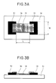
- FIGS. 3A and 3B are illustrative drawings showing the construction of the surface conduction type electron emission element.
- FIG. 4 is a graph showing the relation between the absorption characteristics per arbitrary unit area of the nonevaporable getter and temperature.
- FIG. 5 is a graph showing the relation between the temperature profile of the vessel and press in the vessel in the process before and after the baking treatment in the examples.
- FIG. 6 shows a flow chart in the process in Comparative Example 1.
- FIG. 7 is a graph showing the relation between the temperature profile of the vessel and pressure in the vessel before and after the baking treatment in Comparative Example 1.
- FIG. 8 shows the flow chart in the degassing step in Example 2.
- FIG. 9 is a graph showing the time-dependent changes of electron emission characteristics in Example 2 and in Comparative Example 2.
- FIG. 10 is an illustrative drawing showing the field effect type electron emission element.
- FIG. 11 is a perspective view showing an outline of the image-forming apparatus making use of the field effect type electron emission element formed in Example 3.
- FIG. 12 shows the flow chart of the degassing process in Example 3.
- FIG. 13 is a graph showing the time-dependent changes of the pressure in the vessel manufactured in Example 3 and Comparative Example 3.
- FIG. 14 is a perspective view showing an outline of the image-forming apparatus manufactured in Example 4.
- FIGS. 15A, 15B, 15C, 15D, 15E and 15F are illustrative diagrams showing the process for forming the electron source plate manufactured in Example 4.
- FIGS. 16A and 16B show a pulse waveform preferably used in the activation step of the surface conduction type electron emission element.
- FIGS. 17A and 17B are pulse waveforms preferably used in the forming step of the surface conduction type electron emission element.
- FIG. 18 shows a flow chart of the degassing step in Example 5.
- the image-forming apparatus having a construction as shown in FIG. 2 was manufactured.
- a plurality of surface conduction type electron emission elements - one kind of cold cathode electron emission elements - were formed on the rear plates in this example.
- fluorescent films were provided on the face plate and a color image-forming apparatus with an effective display area having a diagonal length of 15 inches and vertical to transverse length ratio of 3 : 4 was manufactured.
- FIG. 2 is a perspective view showing the outline of the image-forming apparatus used in this example, in which a part of the panel is cut off to show the internal structure.
- the reference numerals 25, 26 and 27 in the drawing correspond to a rear plate, a supporting frame and a face plate, respectively, forming a vessel for maintaining vacuum in the display panel.
- a sealing bonding step is required in order to endow junction among respective members with sufficient strength and airtight property in assembling the vessel.
- the reference numerals 11 and 12 in the drawing denote the evacuation tubes for connecting the vessel to the vacuum pump when the inside of the vessel is evacuated. These evacuation tubes can be utilized as gas-inlet tubes of activation gases when the activation process is executed after the vessel has been assembled.
- a miniature gauge (a total pressure gauge, not shown in the drawing) is attached at the tip of the evacuation tube 11 for evaluating the effectiveness of this example by measuring the pressure in the panel.
- the reference numeral 1 in the drawing shows a nonevaporable getter for maintaining vacuum in the airtight vessel after sealing the evacuation tube.
- the reference numerals 2 and 3 shows electric current input-output terminals for flowing an electric current to the nonevaporable getter. While a nonevaporable getter containing Ti as a main component and comprising Zr, V and Fe was used in this example, a nonevaporable getter containing Zr as a main component may be used.
- the H 2 O absorption characteristics of the nonevaporable getter used in this example is shown in FIG. 4.
- the vertical and horizontal axes denote an evacuation rate and amount of absorption, respectively.
- a through-put method was used for the measurement.
- Characteristics of the nonevaporable getter at room temperature (R.T.), 150°C and 300°C are shown in the graph.
- N ⁇ M pieces of the surface conduction type emission elements 22 are formed on the rear plate 25 to construct a multi-beam source.
- N strings of wiring along the row direction (named as lower wiring) and N strings of wiring along the column direction (named as upper wiring) form a matrix for the N ⁇ M pieces of the surface conduction type emission element.
- FIG. 3A is a top plane view and FIG. 3B is a cross-section view showing the construction of the surface conduction type electron emission element.
- the reference numerals 31, 32 and 33, 34 and 35 in the figures denote a substrate, electrodes, conductive film and an electron emission part, respectively.
- fluorescent films 28 are formed on the bottom face of the face plate 27 . Since the color display device is used in this example, fluorescent substances with R (red), G (green) and B (blue) three primary colors used in CRT are separately coated on the respective fluorescent films 28 .
- a metal-back 29 known, per se, in the art of CRT is provided on the face at the rear plate side of the fluorescent film 28.
- the metal-back 29 is provided in order to improve luminous efficiency by allowing it to serve as a mirror for reflecting a part of the light projected out of the fluorescent film 28 , to protect the fluorescent film 28 from collision of negative ions, to utilize it as an electrode for impressing an electron beam accelerating voltage, and to allow it to serve as an electric current guide for electrons after exciting the fluorescent film 28 .
- the metal-back 29 was formed by subjecting the fluorescent film 28 to smoothing treatment followed by vacuum deposition of Al thereon after forming the fluorescent film 28 on the face plate substrate 27 .
- the metal-back 29 is not needed when a fluorescent film for low acceleration voltage is used for the fluorescent film 28 .
- a transparent conductive film for example ITO film, may be provided between the face plate substrate 27 and fluorescent film 28 , although it was not used in this example.
- the pins represented by the symbols Dox1 to Doxm , Doy1 to Doyn and Hv correspond to terminals provided for putting the airtight vessel as the display panel of this invention into electric continuity with electrical circuits (not shown in the drawing).
- the pins Dox1 to Doxm , Doy1 to Doyn and Hv are electrically connected to the wiring along the row direction 23 of the multi-electron beam source, the wiring along the column direction of the multi-electron beam source and the metal back 29 of the face plate, respectively.
- a rear plate, on which the surface conduction type electron emission elements interconnected into a matrix prior to applying a forming step and adhesives for the supporting plate are formed was manufactured by the steps described above.
- the fluorescent film on which strips of three primary color fluorescent substances are alternately formed and adhesives for the supporting frame were formed on the face plate by the steps as described above.
- the rear plate is held on a X-, Y- and ⁇ - adjustment stage and the rear plate and face plate are heated at a sealing temperature while adjusting the positioning of the face plate.
- the seal temperature depends on the nature of the frit glass, a temperature of 410°C was used for sealing in this example.
- the supporting frame was made to contact with the rear plate and face plate while adjusting their positions with the X-, Y- and ⁇ -adjustment stage. After holding the plates and the supporting frame under a pressure for 10 minutes, the temperature was decreased at a rate of 3°C per minute. When the temperature was reduced by 100°C lower than the sealing temperature, positioning was stopped and the temperature was decreased to room temperature while unlocking the stage.
- the pressure in the vessel manufactured as described above was determined at each step after the degassing step. The results are shown in FIG. 5. The results of pressure measurements obtained when the degassing step was carried out by the following steps are shown in FIG. 7.
- FIG. 5 and FIG. 7 shows that the airtight vessel prepared in Example 1 keeps a lower pressure than the airtight vessel prepared in Comparative Example 1 when the pressure is stabilized after sealing.
- the partial pressure in the airtight vessel was measured with a quadrupole mass spectrometer instead of measuring the total pressure in the vessel.
- the results of oxygen and water partial pressure changes during 24 hours after sealing are shown in TABLE 1. Partial pressure of water Partial pressure of oxygen Example 1 6 ⁇ 10 -10 Pa 5 ⁇ 10 -11 Pa Comparative Example 1 2 ⁇ 10 -9 Pa 1 ⁇ 10 -10 Pa
- This example also gives an image-forming apparatus using the surface conduction type electron emission element (refer to FIGS. 2, 3 and 4 with respect to the image-forming apparatus).
- the rear plate on which the surface conduction type electron emission elements interconnected into a matrix prior to applying a forming step and the adhesives for the supporting frame were formed, was manufactured by the steps described above.
- the fluorescent film on which stripes of three primary color fluorescent films are alternately formed and adhesives for the supporting frame were formed on the face plate by the steps as described above.
- the supporting frame was made to contact with the rear plate and face plate while adjusting their positions with the X-, Y- and ⁇ -adjustment stage. After holding the plates and the supporting frame under a pressure for 10 minutes, the temperature was decreased at a rate of 3°C per minute. When the temperature was reduced by 100°C lower than the sealing temperature, positioning was stopped and the temperature was decreased to room temperature while unlocking the stage.
- FIG. 9 shows that Ie that determines luminance of the fluorescent film, or the electron emission characteristic of the electron source in the image-forming apparatus using the airtight vessel manufactured in this example is more stable with very small deterioration than that in Comparative Example 2.
- An image-forming apparatus using the airtight vessel with the construction as shown in FIG. 10 was manufactured in this example.
- a plurality of field emission elements were formed on the rear plate 111 and providing a spacer 116 between face plate 112 and rear plate 111 as a supporting member to be used under atmospheric pressure in order to make the image-forming apparatus lightweight.
- the face plate 112 is provided with fluorescent films and a color image-forming apparatus with a vertical to transverse length ratio of 3 : 4 whose effective display area has a diagonal length of 10 inches was manufactured.
- the reference numeral 111 denotes a rear plate
- the reference numeral 112 denotes a face plate
- the reference numeral 113 denotes a cathode
- the reference numeral 114 denotes a gate electrode
- the reference numeral 115 denotes an insulation layer between the gate and cathode.
- the reference numeral 112 denotes a face plate
- the reference numeral 123 denotes a supporting frame
- the reference numeral 111 denotes a rear plate
- the reference numeral 116 denotes a spacer in FIG. 11.
- the gap between the face plate 121 and the rear plate 125 is 1.5 mm.
- the reference numeral 126 denotes a nonevaporable getter.
- the rear plate, on which the field emission type electron emission elements interconnected into a matrix for and the adhesives for the supporting frame were formed was manufactured by the steps described above.
- the fluorescent film on which stripes of three primary color fluorescent films are alternately formed and adhesives for the supporting frame were formed on the face plate by the steps as described above.
- the supporting frame was made to contact with the rear plate and face plate while adjusting their positions with the X-, Y- and ⁇ -adjustment stage. After holding the plates and the supporting frame under a pressure for 10 minutes, the temperature was decreased at a rate of 3°C per minute. When the temperature was reduced by 100°C lower than the sealing temperature, positioning was stopped and the temperature was decreased to room temperature while unlocking the stage.
- the pressure in the airtight vessel manufactured as described above was measured at each step after the sealing step. The results are shown in FIG. 13.
- the results of pressure measurements of the airtight vessel prepared by the degassing step as will be described below are also shown in FIG. 13 as a comparative example.
- FIG. 13 shows that the airtight vessel according to this example can attain a high vacuum from the initial stage of evacuation, maintaining a stable high vacuum for a long period of time.
- the pressure remains high from the initial stage of evacuation, showing an abrupt pressure increase at a give time and thereafter. Because the nonevaporable getter was activated after sealing, the gas discharge rate in the airtight vessel becomes larger in the comparative example than in the example, wasting the life span of the nonevaporable getter to result in remarkable deterioration of adsorption ability.
- FIG. 14 An image-forming apparatus using the surface conduction type electron emission device was manufactured in this example (FIG. 14).
- a vessel before sealing the evacuation tubes 11 and 12 is shown in FIG. 14.
- the largest difference between this example and Example 1 is that a forming step and an activation step were applied before manufacturing of vessel by sealing rear plate and face plate.
- the electron source substrate also serves as a rear plate in this example.
- FIG. 14 a process for manufacturing nine surface conduction type electron emission elements is shown in FIG. 15.
- 400 and 1,500 pieces of the electron emission elements along the row direction and column direction, respectively, are arranged on the substrate 21 forming a matrix.
- Step G An electron source substrate prior to subjecting to the forming step was manufactured by the steps described above, wherein the lower wiring 24 , interlayer insulation layers 25 , upper wiring 23 , electrodes 32 and 33 , and conductive films 34 are formed on the substrate 1.
- Step G The electron source substrate 21 prior to subjecting to the forming step prepared as described above was transferred in a chamber (not shown in the drawing). Then, after evacuating the inside of the chamber to a pressure of 1 ⁇ 10 -4 Pa, an electric current was flowed through the electrodes 32 and 33 (energization forming treatment) through each wiring 23 and 24 along the row and column directions, respectively, thereby forming a gap on a portion of each conductive film 34 .
- the voltage waveform to be used in the foregoing forming step is preferably a pulse waveform.
- the pulse wave is generated by either a method in which pulses having a constant voltage at the highest level of the pulse wave are continuously impressed (FIG. 17A) or a method in which the pulse voltage is impressed while increasing the highest level of the pulse wave (FIG. 17B).
- T1 and T2 in FIGS. 17A and 17B represent the pulse-to-pulse distance of the voltage waveform.
- T1 is usually 1 ⁇ sec to 10 msec while T2 is adjusted in a range of 10 ⁇ sec to several hundreds milliseconds.
- a voltage is impressed, for example, for several seconds to several tens of seconds under the conditions as described above.
- the pulse waveform is not limited to a triangular wave but desired waveforms such as a rectangular wave may be used.
- the highest level of the triangular wave may be increased by a desired discrete rate of 0.1 V per one step.
- the pulse with the waveform as shown in FIG. 17B was used in the forming step of this example.
- the pulse intervals of T1 and T2 were 1 msec and 10 msec, respectively, in this example.
- the end point of the forming treatment by an electric current is determined by sensing the resistivity by measuring the electric current when a pulse voltage with a level not locally destroying or deforming the conductive film 34 is inserted among the pulse voltages for the foregoing forming step.
- the forming step by flowing an electric current is completed when the resistance of 1 M ⁇ or more was observed from the measured electric current flowing through the electroconductive film 34 by applying a voltage of about 0.1 V.
- the forming step was completed in this example at the stage when the wave level of the impressed pulse shown in FIG. 17 had reached to about 5 V since the resistance exceeded 1 M ⁇ .
- Carbon films were formed on the substrate among the gaps formed by the forming step and on the conductive films 34 on the periphery of the gaps by this activation treatment.
- the electron emission portion 5 was formed by the steps as hitherto described (FIG. 15F).
- a Zr-V-Fe alloy mainly composed of Zr was used in this example as the non-volatile getter 1 disposed in the vessel.
- Black stripes were formed at first and stripes of the fluorescent films 28 were formed by coating fluorescent substances of each color on the open spaces among the black stripes.
- Fluorescent films with respective colors were exactly positioned on respective electron emission elements before sealing.
- evacuation tubes While two evacuation tubes were used in this example, the number of the evacuation tubes are not limited thereto but four evacuation tubes may be disposed at four corners of the face plate in order to accelerate evacuation speed.
- the vessel was degassed and sealed to form an airtight vessel according to the process shown in FIG. 1.
- the baking temperature is not limited to 300°C but may be higher provided that the frit is not melted or the electron emission element is not damaged by heating.
- the sealing step is executed in this example after the energization activation step requiring organic gases has been completed. Accordingly, adsorption and contamination of organic substances on the inner walls of the vessel and evacuation tubes ascribed to injection of organic substances into the vessel as seen in Example 1 can be avoided, making degassing easy.
- the image-forming apparatus according to this example manufactured by the steps as hitherto described can form stable and high quality images having sufficient luminance for use in television for a long period of time.
- An image-forming apparatus was manufactured in this example by disposing a Ba getter as an evaporable getter in addition to the nonevaporable getter 1 .
- the manufacturing process according to this example includes the same steps A to I as in Example 4.
- a wire-shaped evaporable getter may be used as well.
- the vessel was subjected to degassed and airtight seal steps according to the process shown in FIG. 18.
- the evaporable getter is degassed before the succeeding activation step of the nonevaporable getter in order to prevent the life span of the nonevaporable getter from being shortened by allowing the gases discharged from the evaporable getter to be eliminated by the activated nonevaporable getter.
- the baking temperature was adjusted to 300°C in this example as in Example 4, the baking temperature according to the present invention is not limited to 300°C as will be evident from the foregoing descriptions.
- the evaporable getter is activated (getter flash) at room temperature as described above in order to prevent the function of the getter from being lost due to coagulation of the Ba film after deposition.
- getter flash may be applied at any stage after sealing provided that the Ba film is not coagulated.
- the image-forming apparatus according to this example manufactured by the steps as hitherto described can form stable and high quality images having sufficient luminance for use in television for a long period of time.
- the vessel at a high temperature allows the adsorption time of the deteriorating gases onto the inner wall of the vessel to be largely shortened along with more promptly eliminating the deteriorating gases since the adsorption characteristics of the nonevaporable getter is improved by several times.
- the present invention provides an image-display device with a long life span, making it possible to maintain the electron emission characteristics stable for a long period of time by activating the getter before sealing and by sealing the vessel at a high temperature.
Landscapes
- Engineering & Computer Science (AREA)
- Manufacturing & Machinery (AREA)
- Manufacture Of Electron Tubes, Discharge Lamp Vessels, Lead-In Wires, And The Like (AREA)
- Cathode-Ray Tubes And Fluorescent Screens For Display (AREA)
Applications Claiming Priority (4)
| Application Number | Priority Date | Filing Date | Title |
|---|---|---|---|
| JP13556398 | 1998-05-18 | ||
| JP13556398 | 1998-05-18 | ||
| JP10395599 | 1999-04-12 | ||
| JP11103955A JP3057081B2 (ja) | 1998-05-18 | 1999-04-12 | 気密容器の製造方法および該気密容器を用いる画像形成装置の製造方法 |
Publications (3)
| Publication Number | Publication Date |
|---|---|
| EP0959486A2 true EP0959486A2 (de) | 1999-11-24 |
| EP0959486A3 EP0959486A3 (de) | 2000-05-31 |
| EP0959486B1 EP0959486B1 (de) | 2005-11-09 |
Family
ID=26444519
Family Applications (1)
| Application Number | Title | Priority Date | Filing Date |
|---|---|---|---|
| EP99303818A Expired - Lifetime EP0959486B1 (de) | 1998-05-18 | 1999-05-17 | Verfahren zur Herstellung eines luftdichten Gefässes und eines Bilderzeugungsgerät unter Benutzung dieses Gefässes |
Country Status (5)
| Country | Link |
|---|---|
| US (1) | US6860779B2 (de) |
| EP (1) | EP0959486B1 (de) |
| JP (1) | JP3057081B2 (de) |
| KR (1) | KR100330473B1 (de) |
| DE (1) | DE69928167T2 (de) |
Families Citing this family (9)
| Publication number | Priority date | Publication date | Assignee | Title |
|---|---|---|---|---|
| JP2001035367A (ja) * | 1999-07-21 | 2001-02-09 | Mitsubishi Electric Corp | 陰極線管製造方法および陰極線管製造装置 |
| US6534850B2 (en) * | 2001-04-16 | 2003-03-18 | Hewlett-Packard Company | Electronic device sealed under vacuum containing a getter and method of operation |
| US7091662B2 (en) | 2002-07-23 | 2006-08-15 | Canon Kabushiki Kaisha | Image display device and method of manufacturing the same |
| US7547620B2 (en) * | 2004-09-01 | 2009-06-16 | Canon Kabushiki Kaisha | Film pattern producing method, and producing method for electronic device, electron-emitting device and electron source substrate utilizing the same |
| JP2008527629A (ja) * | 2004-12-30 | 2008-07-24 | イー・アイ・デュポン・ドウ・ヌムール・アンド・カンパニー | ゲッター材料を状態調節する方法 |
| US8173995B2 (en) | 2005-12-23 | 2012-05-08 | E. I. Du Pont De Nemours And Company | Electronic device including an organic active layer and process for forming the electronic device |
| JP2009283295A (ja) * | 2008-05-22 | 2009-12-03 | Canon Inc | 気密容器及び画像表示装置の製造方法 |
| US11552441B2 (en) | 2018-12-06 | 2023-01-10 | Canon Kabushiki Kaisha | Display device and display method |
| WO2020217980A1 (ja) | 2019-04-25 | 2020-10-29 | キヤノン株式会社 | 表示装置、表示装置の制御方法、および制御プログラム |
Family Cites Families (20)
| Publication number | Priority date | Publication date | Assignee | Title |
|---|---|---|---|---|
| BE507222A (de) * | 1950-11-21 | |||
| US4045849A (en) | 1975-08-28 | 1977-09-06 | Rca Corporation | Method for assembling a thermally-set getter spring in a CRT |
| JPS5364461A (en) | 1976-11-22 | 1978-06-08 | Toshiba Corp | Exhaustion method of fluorescent display tube |
| KR940007250B1 (ko) | 1991-11-22 | 1994-08-10 | 삼성전관 주식회사 | 형광표시판 제조방법 |
| JP3056941B2 (ja) | 1994-04-28 | 2000-06-26 | キヤノン株式会社 | 画像表示装置の製造方法 |
| JP3121200B2 (ja) | 1994-04-28 | 2000-12-25 | キヤノン株式会社 | 画像表示装置の製造方法 |
| JP2832510B2 (ja) | 1994-05-10 | 1998-12-09 | 双葉電子工業株式会社 | 表示装置の製造方法 |
| JP3222357B2 (ja) | 1994-06-09 | 2001-10-29 | キヤノン株式会社 | 画像形成装置及びその製造方法 |
| US5453659A (en) * | 1994-06-10 | 1995-09-26 | Texas Instruments Incorporated | Anode plate for flat panel display having integrated getter |
| JP3305166B2 (ja) | 1994-06-27 | 2002-07-22 | キヤノン株式会社 | 電子線装置 |
| JP3062023B2 (ja) | 1994-12-19 | 2000-07-10 | キヤノン株式会社 | 真空外囲器および画像表示装置 |
| EP0955662B1 (de) * | 1995-03-13 | 2006-01-25 | Canon Kabushiki Kaisha | Herstellungsverfahren einer Elektronenquelle und eines Bilderzeugungsgeräts |
| US5697825A (en) * | 1995-09-29 | 1997-12-16 | Micron Display Technology, Inc. | Method for evacuating and sealing field emission displays |
| JP3222397B2 (ja) | 1995-12-19 | 2001-10-29 | キヤノン株式会社 | 画像表示装置 |
| US5688708A (en) * | 1996-06-24 | 1997-11-18 | Motorola | Method of making an ultra-high vacuum field emission display |
| US5681198A (en) | 1996-10-15 | 1997-10-28 | Industrial Technology Research Institute | Vacuum seal method for cathode ray tubes |
| JPH10134721A (ja) | 1996-10-28 | 1998-05-22 | Ind Technol Res Inst | 陰極線管の真空密封方法 |
| DE958589T1 (de) | 1996-12-12 | 2000-08-17 | Candescent Technologies Corp., San Jose | Lokale energieaktivation eines getters |
| JP2962270B2 (ja) | 1997-04-03 | 1999-10-12 | 日本電気株式会社 | 陰極線管の製造方法 |
| KR19990027714A (ko) | 1997-09-30 | 1999-04-15 | 김영남 | 게터 챔버를 이용한 전계방출표시소자의 이차 진공방법 |
-
1999
- 1999-04-12 JP JP11103955A patent/JP3057081B2/ja not_active Expired - Fee Related
- 1999-05-11 US US09/309,766 patent/US6860779B2/en not_active Expired - Fee Related
- 1999-05-17 DE DE69928167T patent/DE69928167T2/de not_active Expired - Lifetime
- 1999-05-17 KR KR1019990017541A patent/KR100330473B1/ko not_active Expired - Fee Related
- 1999-05-17 EP EP99303818A patent/EP0959486B1/de not_active Expired - Lifetime
Also Published As
| Publication number | Publication date |
|---|---|
| KR100330473B1 (ko) | 2002-04-01 |
| US6860779B2 (en) | 2005-03-01 |
| EP0959486A3 (de) | 2000-05-31 |
| JP3057081B2 (ja) | 2000-06-26 |
| DE69928167D1 (de) | 2005-12-15 |
| KR19990088327A (ko) | 1999-12-27 |
| DE69928167T2 (de) | 2006-06-08 |
| EP0959486B1 (de) | 2005-11-09 |
| US20020042240A1 (en) | 2002-04-11 |
| JP2000040469A (ja) | 2000-02-08 |
Similar Documents
| Publication | Publication Date | Title |
|---|---|---|
| EP0836213B1 (de) | Bilderzeugungsgerät | |
| US6506089B2 (en) | Manufacturing method of image forming apparatus, manufacturing apparatus of image forming apparatus, and manufacturing method of panel apparatus | |
| US7271529B2 (en) | Electron emitting devices having metal-based film formed over an electro-conductive film element | |
| US7034449B2 (en) | Image display apparatus and method of manufacturing the same | |
| US6860779B2 (en) | Method for manufacturing airtight vessel and image-forming apparatus using airtight vessel | |
| JP3332906B2 (ja) | 画像形成装置の製造方法 | |
| JP3397520B2 (ja) | 電子源、表示パネルおよび画像形成装置ならびにそれらの製造方法 | |
| JP3639774B2 (ja) | 画像形成装置の製造方法 | |
| JP3639762B2 (ja) | 画像形成装置の製造装置 | |
| JPH0883579A (ja) | 画像形成装置およびその製造方法 | |
| JP3437337B2 (ja) | 表面伝導型電子放出素子の製造方法 | |
| JP3423524B2 (ja) | 電子放出素子の製造方法 | |
| JPH0950241A (ja) | 画像形成装置 | |
| JP3416295B2 (ja) | 画像形成装置の製造装置および画像形成装置の製造方法 | |
| JPH08162009A (ja) | 電子放出素子および該素子を用いた電子源および画像形成装置ならびにそれらの製造方法 | |
| JP3135801B2 (ja) | 画像形成装置の製造方法 | |
| JP3174482B2 (ja) | 電子放出素子を用いた画像形成装置の作製方法 | |
| JP2000251788A (ja) | 画像形成装置及びその製造方法 | |
| JPH10302676A (ja) | 画像形成装置 | |
| JPH08180819A (ja) | 真空排気容器およびそれを具備した画像表示装置 | |
| JPH08160881A (ja) | 表面伝導型電子放出素子、電子源基板および画像形成装置ならびにそれらの製造方法 | |
| JPH08329836A (ja) | 電子放出素子及び画像形成装置の製造方法 | |
| JP2000195425A (ja) | 画像形成装置の製造方法 | |
| JP2004029775A (ja) | 画像形成装置 | |
| JPH0845417A (ja) | 電子放出素子、電子源、及びそれを用いた画像形成装置と、それらの製造方法 |
Legal Events
| Date | Code | Title | Description |
|---|---|---|---|
| PUAI | Public reference made under article 153(3) epc to a published international application that has entered the european phase |
Free format text: ORIGINAL CODE: 0009012 |
|
| AK | Designated contracting states |
Kind code of ref document: A2 Designated state(s): DE FR GB IT NL |
|
| AX | Request for extension of the european patent |
Free format text: AL;LT;LV;MK;RO;SI |
|
| PUAL | Search report despatched |
Free format text: ORIGINAL CODE: 0009013 |
|
| AK | Designated contracting states |
Kind code of ref document: A3 Designated state(s): AT BE CH CY DE DK ES FI FR GB GR IE IT LI LU MC NL PT SE |
|
| AX | Request for extension of the european patent |
Free format text: AL;LT;LV;MK;RO;SI |
|
| 17P | Request for examination filed |
Effective date: 20001020 |
|
| AKX | Designation fees paid |
Free format text: DE FR GB IT NL |
|
| 17Q | First examination report despatched |
Effective date: 20030611 |
|
| GRAP | Despatch of communication of intention to grant a patent |
Free format text: ORIGINAL CODE: EPIDOSNIGR1 |
|
| GRAS | Grant fee paid |
Free format text: ORIGINAL CODE: EPIDOSNIGR3 |
|
| GRAA | (expected) grant |
Free format text: ORIGINAL CODE: 0009210 |
|
| AK | Designated contracting states |
Kind code of ref document: B1 Designated state(s): DE FR GB IT NL |
|
| PG25 | Lapsed in a contracting state [announced via postgrant information from national office to epo] |
Ref country code: IT Free format text: LAPSE BECAUSE OF FAILURE TO SUBMIT A TRANSLATION OF THE DESCRIPTION OR TO PAY THE FEE WITHIN THE PRESCRIBED TIME-LIMIT;WARNING: LAPSES OF ITALIAN PATENTS WITH EFFECTIVE DATE BEFORE 2007 MAY HAVE OCCURRED AT ANY TIME BEFORE 2007. THE CORRECT EFFECTIVE DATE MAY BE DIFFERENT FROM THE ONE RECORDED. Effective date: 20051109 |
|
| REG | Reference to a national code |
Ref country code: GB Ref legal event code: FG4D |
|
| REF | Corresponds to: |
Ref document number: 69928167 Country of ref document: DE Date of ref document: 20051215 Kind code of ref document: P |
|
| ET | Fr: translation filed | ||
| PLBE | No opposition filed within time limit |
Free format text: ORIGINAL CODE: 0009261 |
|
| STAA | Information on the status of an ep patent application or granted ep patent |
Free format text: STATUS: NO OPPOSITION FILED WITHIN TIME LIMIT |
|
| 26N | No opposition filed |
Effective date: 20060810 |
|
| PGFP | Annual fee paid to national office [announced via postgrant information from national office to epo] |
Ref country code: NL Payment date: 20090527 Year of fee payment: 11 |
|
| PGFP | Annual fee paid to national office [announced via postgrant information from national office to epo] |
Ref country code: FR Payment date: 20090520 Year of fee payment: 11 |
|
| REG | Reference to a national code |
Ref country code: NL Ref legal event code: V1 Effective date: 20101201 |
|
| REG | Reference to a national code |
Ref country code: FR Ref legal event code: ST Effective date: 20110131 |
|
| PG25 | Lapsed in a contracting state [announced via postgrant information from national office to epo] |
Ref country code: NL Free format text: LAPSE BECAUSE OF NON-PAYMENT OF DUE FEES Effective date: 20101201 |
|
| PG25 | Lapsed in a contracting state [announced via postgrant information from national office to epo] |
Ref country code: FR Free format text: LAPSE BECAUSE OF NON-PAYMENT OF DUE FEES Effective date: 20100531 |
|
| PGFP | Annual fee paid to national office [announced via postgrant information from national office to epo] |
Ref country code: GB Payment date: 20130523 Year of fee payment: 15 Ref country code: DE Payment date: 20130531 Year of fee payment: 15 |
|
| REG | Reference to a national code |
Ref country code: DE Ref legal event code: R119 Ref document number: 69928167 Country of ref document: DE |
|
| GBPC | Gb: european patent ceased through non-payment of renewal fee |
Effective date: 20140517 |
|
| REG | Reference to a national code |
Ref country code: DE Ref legal event code: R119 Ref document number: 69928167 Country of ref document: DE Effective date: 20141202 |
|
| PG25 | Lapsed in a contracting state [announced via postgrant information from national office to epo] |
Ref country code: DE Free format text: LAPSE BECAUSE OF NON-PAYMENT OF DUE FEES Effective date: 20141202 |
|
| PG25 | Lapsed in a contracting state [announced via postgrant information from national office to epo] |
Ref country code: GB Free format text: LAPSE BECAUSE OF NON-PAYMENT OF DUE FEES Effective date: 20140517 |