EP0959470A1 - Calibrage d'égalisation d'ecriture dans un dispositif de stockage de données - Google Patents
Calibrage d'égalisation d'ecriture dans un dispositif de stockage de données Download PDFInfo
- Publication number
- EP0959470A1 EP0959470A1 EP99303793A EP99303793A EP0959470A1 EP 0959470 A1 EP0959470 A1 EP 0959470A1 EP 99303793 A EP99303793 A EP 99303793A EP 99303793 A EP99303793 A EP 99303793A EP 0959470 A1 EP0959470 A1 EP 0959470A1
- Authority
- EP
- European Patent Office
- Prior art keywords
- current
- data storage
- amplitude
- write
- storage medium
- Prior art date
- Legal status (The legal status is an assumption and is not a legal conclusion. Google has not performed a legal analysis and makes no representation as to the accuracy of the status listed.)
- Granted
Links
Images


Classifications
-
- G—PHYSICS
- G11—INFORMATION STORAGE
- G11B—INFORMATION STORAGE BASED ON RELATIVE MOVEMENT BETWEEN RECORD CARRIER AND TRANSDUCER
- G11B20/00—Signal processing not specific to the method of recording or reproducing; Circuits therefor
- G11B20/10—Digital recording or reproducing
- G11B20/10009—Improvement or modification of read or write signals
- G11B20/10046—Improvement or modification of read or write signals filtering or equalising, e.g. setting the tap weights of an FIR filter
- G11B20/10194—Improvement or modification of read or write signals filtering or equalising, e.g. setting the tap weights of an FIR filter using predistortion during writing
-
- G—PHYSICS
- G11—INFORMATION STORAGE
- G11B—INFORMATION STORAGE BASED ON RELATIVE MOVEMENT BETWEEN RECORD CARRIER AND TRANSDUCER
- G11B5/00—Recording by magnetisation or demagnetisation of a record carrier; Reproducing by magnetic means; Record carriers therefor
- G11B5/02—Recording, reproducing, or erasing methods; Read, write or erase circuits therefor
- G11B5/09—Digital recording
Definitions
- the present invention relates to improvements to an apparatus for writing data to a magnetic tape data storage device for improving the rate at which data may be written to tape, and particularly although not exclusively to a calibration method for such an apparatus.
- the magnetic media may comprise a flexible elongate tape which is coated with a magnetic material and which is wound between two reels past a magnetic write head.
- the magnetic media may also comprise a rigid disk which is coated with a magnetic medium and data is recorded to the disk by moving a recording head in a radial direction across the disk while the disk is rotated about its center.
- data may be recorded using a plurality of write heads and is read with a plurality of read heads.
- write and read heads may be either substantially stationary with respect to the rest of the device in which case data are stored in a plurality of tracks parallel to the elongate direction of the tape or the write and read heads may be mounted on a drum which is rotated about an axis at an angle to the elongate direction of the tape, in which case the data are stored in a series of tracks diagonally across the magnetic tape.
- recording heads are fabricated from ferrite which is a sintered combination of a ferro magnetic material and a ceramic combined to yield a material with the high magnetic permeability of the former and the high electrical resistance of the latter.
- ferrite which is a sintered combination of a ferro magnetic material and a ceramic combined to yield a material with the high magnetic permeability of the former and the high electrical resistance of the latter.
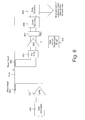
- a solid line 110 a plot indicating how an output signal of a ferrite write head decreases as the frequency of a driving write current signal of constant amplitude increases.
- the output signal for a given input current drops significantly at a "roll off" frequency 120 which is, typically of the order 30 - 40 MHz. This limits an effective maximum write rate of the ferrite head to the order 80 MBits/s. It is known to attempt to correct for this roll off in the frequency response of a write head by preferentially boosting high frequencies in the write current according to a curve such as illustrated by a dashed line 130 in Fig. 1.
- WPE Write Pre-Equalization
- write drivers in digital magnetic data stored systems are highly non-linear devices.
- Conventional write drivers comprise switches which send two polarities of current to the write heads in order to record two distinct magnetization states on the magnetic media.
- Ampex produced a write pre-equalization scheme which comprised a linear amplifier current driver i.e.
- the output signal of the write driver was proportional to the input signal to the write driver.
- the Ampex scheme applied a boost to the frequency response of the write driver to compensate for the frequency response to the write head.
- the Ampex implementation of write pre-equalization required substantial power, typically of the order 15 Watts, and could only be produced using discrete components. Hence it is not possible to implement this as a single application specific integrated circuit (ASIC).
- the Ampex scheme was also difficult to set up.
- the magnetization of the medium changes direction during the time that the magnetic field is increasing in magnitude from zero. If, at the time of the negative going edge in the recording head driver current, the magnetic field has not yet risen to its steady-state level then the next magnetic transition occurs slightly earlier than if the magnetic field had been at (or closer to) the steady-state level. This causes the physical location on a magnetic data storage medium at which the magnetization of the medium changes direction to be "advanced", or moved closer to the previous transition. Hence, positions of magnetic field transitions on a magnetic data storage medium may be laterally displaced. This lateral displacement of magnetization on the magnetic recording medium is also known herein as "bit shift”, "peak shift” and "transition shift".
- the size of the transition shift depends in a non-linear way on the magnetic field level when last current transition occurred, and hence on the duration of the previous current pulse relative to the finite risetime of the record head's magnetic field.
- the ongoing pressure in the development of new magnetic data storage systems is to increase the data storage capacity of any said data storage media.
- By increasing the effective bandwidth of the write head in a magnetic data storage system it is possible to increase the bit rate at which data is written to, for example, magnetic tapes and hence increase the storage capacity of the tape.
- Specific embodiments and methods according to the present invention aim to provide a method for set up and optimization of a means of compensating for a frequency response roll-off in a write channel of a magnetic data storage system.
- a method of optimizing a write channel in a data storage device characterized by said write channel comprising:
- each of said first amplitude, said delay period and said second amplitude are independently variable.
- said output signal of said write channel is produced in response to an input test signal, and suitably, said method comprises performing said steps (i), (ii) and (iii) for each of a plurality of test signals.
- a data storage device having a write channel comprising:
- a data storage device configured to write data to a data storage medium said data storage device having a write channel characterized by comprising:
- each said variable is adjustable independently of each other said variable.
- the invention includes a method of optimizing a write channel in a data storage device configurable to write data to a data storage medium, said method comprising the steps of:
- said low frequency test signal comprises a "4T" pattem.
- Said quality metric may comprise a signal-to-noise ratio, or bit error rate.
- said predetermined value of delay is set in the range 1 / 5 to 4 / 5 of the minimum bit period at which said data are written to said data storage medium and suitably at around 1 / 3 of said minimum bit period.
- said predetermined value of delay is set in the range 1.8 to 7.2 nanoseconds and suitably at around 3.5 nanoseconds. Said predetermined value of delay in the best mode, lies within the range 1.8 to 7.2 nanoseconds.
- said mixed frequency test signal comprises a pseudo random pattern.
- said mixed frequency test signal comprises a "1T" bit pattem.
- the invention includes a method of writing data to a data storage medium, through a write channel comprising a first transconductor, a delay device and a second transconductor, said method comprising the steps of:
- said data is preferably replaced by a test signal.
- a frequency of said test signal is varied.
- said step of optimizing said variables comprises the steps:
- the data storage medium may comprise a magnetic tape, a magnetic disk or the like.
- the best mode herein relates to a Digital Data Storage system (DDS) based on the digital audio tape system (DAT) being a helical scan system.
- DDS Digital Data Storage system
- DAT digital audio tape system
- the tape data storage system presented herein may advantageously implement one particular version of the DDS system namely the DDS4 standard which is still under development.
- the methods and apparatus disclosed herein are not restricted to systems having rotating heads or to systems where digital data are stored on tape.
- a channel ASIC 200 provides a source of logic signals which are to be recorded on to a tape according to the best mode presented herein.
- the channel ASIC 200 converts a stream of digital data from the host device into streams of digital data write signals 206 and 207 with appropriate voltage levels to input into a write driver 201.
- Data stream 207 is an inverted version of data stream 206.
- the process of inverting a digital signal comprises replacing every instance of the digital signal which represents binary digit "0" with a digital signal that represents binary digit "1” and replacing every instance of the digital signal which represents a binary digit "1" with a digital signal representing binary digit "0".
- the voltage levels output by channel ASIC 200 conform to the voltage levels conventionally used in known pseudo emitter coupled logic (PECL).
- the two logic states are typically represented by a differential voltage swing of 1V peak-to-peak.
- PECL has, typically, the same differential voltage swings as conventional emitter coupled logic (ECL) but have been translated by +5V.
- PECL is a well known way of transferring logic signals where the timing of such signals is critical.
- the write signals 206 and 207 are input to the double pulse write driver 201.
- the write driver 201 outputs conventional write current signals set by extemal reference currents 210 and 211.
- Write currents 212 and 213 output from write driver 201 have an extra narrow pulse of current added on each transition according to one aspect of the present invention. The width of this narrow current pulse is set by an external reference current and an extemal resistor or capacitor.
- the write current 212 and 213 are input to a multiplexor 202 which switches the write current between the two write heads 204 and 205 via a coupling 203 and transformers 208 and 209.
- the coupling 203 comprises a connection between the physical location of the double pulse write driver as described herein and either the transformers 208 and 209 or the write heads 204 and 205.
- Driver current 301 is produced by a first transconductor circuit 400 which produces two write output signals in response to two input signals.
- the output signals of the first transconductor are amplified versions of the write signals 206 and 207 input into first transconductor 400.
- the input signals are also input to a delay unit 402, the outputs of the delay unit being input to a second transconductor 401.
- Write signals 206, 207 input to first and second transconductors respectively each comprise a digital logic voltage signal. Outputs of the first and second transconductors comprise current signals.
- Each transconductor comprises a buffer, a switch and a current amplifier source, the combination of buffer, switch and current amplifier source operating to receive a said voltage logic signal and output a current pulse drive signal of predetermined and controlled current value.
- To the main driver current 301 is added an inverted and delayed driver current 302.
- the amplitude of the pulses in the driver current and delay current are represented in Fig. 3 herein as IH and IH_delayed, respectively.
- the amplitudes of main driver current 301 and delayed current driver 302, IH and IH_delayed respectively, are set by the reference currents 210 and 211 and may be preset.
- the driver current 301 and delayed current 302 are added to produce a modified write signal 212, head current.
- the effect of adding the delayed inverted current 302 to driver 301, if IH_delayed is less than IH, is to produce a respective double pulse current spike corresponding to each transition of the main driver current.
- the double pulse comprises a narrow pulse which has a positive going edge which is coincident with a positive going edge of the driver current 301 followed by a pulse spike having a lower amplitude but being of longer duration.
- At each negative going edge of the main driver current there is a coincident negative going narrow pulse in the sum current.
- the positive going and negative going narrow pulse spikes are of a same duration.
- the narrow pulse which is also known herein as the pulse current I_pulse has an amplitude 304 which is equal to (IH+IH_delayed) 2 similarly, the pulse spike having a lower amplitude having a lower amplitude but being of longer duration which is also known herein as the main current or I_main has an amplitude 303 which may be represented by the following equation (IH-IH_delayed) 2
- both the pulse current and main current are independently adjustable to produce an optimum performance of the write pre-equalisation.
- the narrow pulse contributes significantly to the high frequency components of the sum (head) current 212.
- These additional high frequency components in the write current partially compensate for the roll-off in the frequency response of the write head at approximately 40 MHz.
- the additional high frequency components added to the write current result in an improved effective bandwidth of the write heads, and as a result may increase the roll off in the response of the write channel as a whole, including the write head, from approximately 40 MHz up to approximately 80MHz.
- an initial narrow pulse at a positive going edge of a pulse of the sum head current may be configured such that, irrespective of the duration of the head pulse ie 1T, 2T, 3T or 4T, the magnetic field generated across the head gap of the recording head is at a substantially same value whenever a negative going edge of the sum head current is encountered. Ensuring that a decreasing magnetic field in the recording head gap always starts from a substantially same value of field strength allows the occurrence of "bit shift" as described hereinbefore to be minimized.
- the initial narrow current pulse results in a more rapidly increasing magnetic field than in the case of a conventional driver current pulse. The more rapid increase in the magnetic field generated in response to the sum head current is to ensure that the resulting magnetic field is at a correct, pre-determined level in time for a negative going edge of a sum head current to initiate a decrease in magnetic field.
- the double pulse write driver 201 and multiplexer 202 are implemented on a single application specific integrated circuit (ASIC).
- ASIC application specific integrated circuit
- the two logical signals WriteP 206 and WriteN 207 from Channel ASIC 200, are written to amplifier 400.
- logical signals writeP 206 and writeN 207 are written to delay unit 402.
- the delay circuit stores and delays logical signals 206 and 207 for a short period of time. The delay period is designed to be easily adjustable and calibrated either by changing the value of a single resistor or capacitance external to the ASIC.
- the optimal time by which the logical signals should be delayed is found to be of the order of 3.5 ns where the bit period is 9 ns.
- the delayed logical signals are written to transconductor 401.
- transconductors 400 and 401 have substantially similar properties.
- Transconductors 400 and 401 are both conventional.
- the electronic circuitry comprising amplifier 401 is preferably a direct copy of the electronic circuitry comprising amplifier 400.
- the delayed logical signals are read out from amplifier 401 and are combined with the output of transconductor 400 prior to sending to write multiplexer 202.
- the output signals of second transconductor 401 and first transconductor 400 are combined in the following manner.
- the driver current 301 is added to delayed current 302 and inverted delayed driver current 406 is added to delayed driver current 405 yielding the respective head currents 212 and 213 which are used to drive the write heads.
- the head current 212 and its inverted counterpart 213 are written to the write multiplexer 202.
- the write multiplexer switches the sum currents 212 and 213 between two write heads according to switching signals 408.
- Write current 212 is switched between inputs WHAP and WHBP which correspond to the two write heads 204 and 205.
- write current 213 are switched between inputs WHAN and WHBN.
- a "write pass" is defined as a single passage of the tape past a write head for writing onto a single track, irrespective of whether the tape speed varies, or whether the tape stops during a pass.
- a write pass may comprise a sequence of writes which cause data to be written in a sequence along one or more tracks, which are themselves written in sequence. Whilst a write channel serving two write heads is shown in the best mode herein, the invention applies equally to a write channel having a single write head, or any other plurality of write heads.
- FIG. 5 there is illustrated schematically an example of an H-Bridge write driver circuit according to the best mode presented herein.
- the input signals WD and WD inv correspond with the logical signals 206 and 207 respectively.
- the outputs of the H-Bridge circuit comprise the driver currents 301 and 405.
- an additional H-Bridge circuit according to the present invention described herein.
- the additional H-Bridge circuit receives the delayed logical signals WD_DEL and WD_DEL inv which are the delayed versions of logical signals 206 and 207 respectively after having been read from the output of delay unit 402.
- the amplitudes of the driver currents 301 and 405 and the delayed driver currents 406 and 302 which are combined before sending to the write heads are set by reference current IW x K1 and IW-Pulse X K2.
- K 1 and K 2 are constants chosen to ensure that driver currents 301 and 405 have larger amplitudes than the delayed currents 406 and 302.
- driver currents signals WD, WD inv , and delayed currents WD_DEL and WD_DEL inv are illustrated schematically driver currents signals WD, WD inv , and delayed currents WD_DEL and WD_DEL inv .
- the time delay introduced by delay unit 402 is indicated by t_delay 620.
- the driver currents signals have a finite rise time which is the time taken for the current to change from the value representing binary digit "0" to the current representing binary digit "1". The same finite transition time is observed for the transition from binary digit "1" to binary digit "0".
- One of the key requirements of the write driver is to minimize the rise time of the driver currents. Typical values of the expected range in write current according to the best mode herein are 30 mA to 100 mA. Typically, a write head having inductance of the order 100 to 200 mH may be used.
- FIG. 7 there is illustrated schematically a signal processing diagram for processing of the host data signals into a form which includes frequency components which compensate for a higher frequency roll off of the ferrite write head.
- Incoming host data signals in the form of bit pulses are split into first and second signal paths, the first path being amplified/buffered in first transconductor 400 by a first degree of amplification 700.
- the second signal path of host data signals is delayed by delay device 402 for a predetermined delay period, which may be varied by adjustment.
- the delayed host data signals are amplified/buffered in second transconductor 401, which also inverts the delayed host data signals and amplifies the host data signals by a second degree of amplification, the second degree of amplification being less than the first degree of amplification.
- the inverted delayed data signals are summed 704 with the amplified host data signal to produce a modified write signal as illustrated by sum (head) current 212 in Fig. 3 herein.
- the modified write signal is of the form described hereinabove, containing a relatively short higher amplitude pulse current on a leading edge of each main current pulse, which introduces higher frequency components which compensate for a higher frequency roll off of the write head.
- the modified data write signal is written to the tape data storage medium via the write head 705.
- the resultant data signals written to the tape data storage medium may be better defined and have a better signal to noise ratio and/or a lower bit error rate than in the prior art case.
- the write driver addresses the problem of the roll-off in the frequency response of ferrite recording heads in magnetic data storage devices.
- the write driver described herein requires that three separate variables, amplitude of the pulse current I_pulse 304, the amplitude of the main current I_main 303 and the width of the pulse current t_delay 620 are all chosen so as to optimize the effective frequency response of the write channel using the WPE method and apparatus scheme described.
- the process of calibrating a write driver requires optimizing the operation of the write driver such that, for example, the number of errors occurring when data are written to tape are minimized.
- Conventional write drivers have typically only one variable to optimize during a calibration process.
- Such a calibration process would conventionally comprise writing data to tape, then reading the data from tape and analyzing a quality metric which is a measure of the quality of the writing process.
- the quality metric may be typically a measure of the bit error rate, ie the proportion of incorrectly written bits of data introduced during the write operation.
- bit error rates in prior art schemes are, before error correction, of the order 1 in 10 5 - 10 6 bits in tape drives, whilst bit rate errors incurred in write operations in disk drives are typically lower than for tape drives.
- Another quality metric typically used to assess the write operation in writing data to a data storage medium is signal-to-noise ratio.
- bit error rate (BER) and/or signal-to-noise (SNR) are used to assess a write operation.
- BER bit error rate
- SNR signal-to-noise
- calibration can involve writing standard signals to tape while sweeping a single variable through all possible values of that variable whilst monitoring a quality metric of the resulting written data.
- the write driver described herein operates a modified data write signal as illustrated in Fig. 3 herein having a head current a pulse current of a first amplitude and duration followed by a second portion by a main current of a second amplitude and duration.
- three variables are present, being an amplitude of the pulse current I_pulse 304, a width of the pulse current t_delay 620, and an amplitude of the main current signal I_main 303.
- calibration of the driver circuitry to produce optimized performance becomes a complex problem to solve. If there are of the order 10 possible values of each of the variables then there are of the order 10 3 possible calibration points.
- a tape data storage device configured to write data to an elongate tape using a write head 803 and to recover said data from tape using a read head 804.
- the tape data storage device as illustrated in Fig. 8 is configured to write a plurality of test signals to tape via a write channel, read the test signals from tape via a read channel and measure a quality metric of the write operation according to the present invention described herein.
- Data generator 800 feeds logic signals to WPE write driver 801 which drives the write head 803 as described herein before.
- WPE write driver 801 drives the write head 803 as described herein before.
- a plurality of data pattems generated by data generator 800 are written to tape.
- the plurality of data pattems are test signals which can be used to yield a quality metric of the writing process.
- the test signals written to tape are read back from tape using read head 804.
- the signals read off tape pass through pre-amplifier 805, variable gain amplifier 806 which is set to "fixed gain” mode, filter 807, clock signal recovery stage 808, and data recovery stage 809.
- the variable gain amplifier 806 in the read channel is set to "fixed gain” mode which means that the amplification applied to test signals read back from tape is substantially constant with frequency.
- BER bit error rate
- SNR signal-to-noise ratio
- the calibration method described herein comprises optimizing the write channel to write low-frequency signals to tape and then optimizing the write channel whilst writing mixed frequency signals to tape.
- an objective of calibration of the compensation means is to approximate an optimum high frequency amplification applied to the write current as shown by the dotted line in Fig. 1 as closely as possible by variation of the three variable parameters of main drive current signal amplitude, delay period and delayed main drive current signal amplitude.
- a correctly calibrated WPE driver adjusted to accurately compensate for the high frequency roll off of a write head should yield a substantially same value of quality metrics when writing both low frequency data, which is unaffected by the roll-off of the recording head, and high frequency data, which is subject to the high frequency roll off of the write head.
- Another objective of calibration of the compensation means is to ensure that a changing magnetic field generated by a record head in response to a positive going edge of a driver current rises to a same value irrespective of a time duration of the driver current pulse, ie 1T, 2T, 3T or 4T. Ensuring that the magnetic field rises to a fixed value irrespective of the duration of the driver current pulse initiating the rising magnetic field reduces the occurrence of lateral displacement of changes in magnetization direction on the magnetic data storage medium. Minimizing relative lateral displacements between pulses recorded on magnetic data storage medium minimizes the occurrence of timing errors during a subsequent read operation and thereby minimizes the measured bit error rate.
- the low frequency test signal written to tape as part of the calibration procedure for the WPE driver is a "4T" pattern 910.
- the 4T pattern has a pulse duration of 4 x f b seconds where 1 /f b 920 is the bitrate at which data are written to tape during the normal operation of the tape data storage device described herein.
- the 4T pattem has a frequency which is one quarter of the maximum frequency which is written to tape.
- the 4T pattern should be of low enough frequency that, when writing to tape, it is unaffected by transient effects resulting from, for example, the finite rise time of the magnetic field in the write heads.
- the optimal values of the quality metrics derived from writing a 4T pattern to tape can be used as a standard for comparison with the quality metrics of writing mixed frequency test signals to tape.
- the WPE driver has three independently adjustable variables, all of which must be optimized in order to optimally compensate for the roll-off of the write head.
- the three variables are: the value or amplitude of the pulse current, I_pulse 304; the value or amplitude of the main current, I-main 303; and the width of the pulse current, t_delay 620.
- the specific method as described herein comprises "removing" one of the variables by writing a 4T pattem to tape and optimizing the amplitudes of the main current 303.
- the process of optimization refers to finding the value of a variable which maximizes one or more quality metrics during a write operation.
- a high frequency 1T, bit pattern is recorded and an optimal pulse current is found.
- a mixed frequency, pseudo-random bit pattem 930 is recorded and an optimal pulse current amplitude is found.
- step 1010 the amplitude of the pulse current, 304 is set to its respective minimum value.
- the width of the pulse current is set to a pre-determined fixed value.
- step 1020 the data generator 800 is configured to output a 4T pattern.
- the main current, I-main is set to its minimum value, and the 4T pattern is written to tape.
- step 1030 the 4T pattem written to tape using write head 803 is read back from tape via write head 804.
- the low frequency 4T pattern is recovered from the data read off tape and the quality metrics signal-to-noise ratio and/or bit error rate associated with the value of the main driver current used to write the data are measured.
- the gain of amplifier 400 is increased and the low frequency 4T pattem is again written to tape.
- the quality metrics associated with the new, increased main current are measured and the process of changing the main current level, recording low frequency pattem to tape and measuring the quality metrics associated with that driver current are repeated until the main current level that maximizes SNR and/or minimizes BER is found.
- the main current is fixed at a level which optimizes the values for the quality metrics used to assess the write performance.
- a pseudo-random bit pattern used in calibrating the WPE driver comprises a pseudo-random mixture of 1T, 2T, 3T, 4T transitions.
- the pseudo-random bit pattem contains a mix of frequencies.
- the invention is not limited to methods and apparatus using pseudo-random pattems to calibrate the WBE driver and that other random or quasi-periodic bit pattems could be employed.
- step 1050 the optimum level of main current, I-main, for recording low frequency, 4T, patterns to tape is found.
- the time delay t_delay which is the width of the pulse current is fixed at a value of the order 1 / 3 f b seconds where f b is the bit period at which data are written to tape according to the best mode described herein.
- the bit period f b is 9 nanoseconds. It has been found experimentally that the pulse current, 303, and the width of the pulse current, t_delay, are not truly independent variables.
- t_delay can be fixed at an optimal value and hence it only remains to find the value of the pulse current amplitude 303 which maximizes the quality metrics in order to complete the calibration of the WPE driver.
- t_delay is set to of the order 1 / 5 - 4 / 5 of the bit period f b .
- the pulse current amplitude 303 is set to its minimum value and the generator 800 is configured to generate a pseudo-random bit pattern which is recorded to tape.
- the pseudo-random test signal is read back from tape and the quality metrics SNR and/or BER are measured for the mixed frequency test signal.
- step 1140 the quality metrics are monitored as the pseudo-random bit pattern is recorded to tape whilst the pulse current amplitude is gradually increased.
- An optimal pulse current value which maximizes the quality metrics whilst recording a mixed frequency signal is found, completing the calibration of the WPE driver.
- the specific method described herein above encompasses varying a single one of the three variables through a plurality of values whilst maintaining other ones of the variables at fixed values, and for each value of variable, determining a quality metric of a corresponding output of the write channel as written to tape.
- a value of variable which produces a write channel output which when written to tape and read by the read channel produces an optimum quality metric is selected.
Priority Applications (1)
| Application Number | Priority Date | Filing Date | Title |
|---|---|---|---|
| EP19990303793 EP0959470B1 (fr) | 1998-05-19 | 1999-05-14 | Calibrage d'égalisation d'ecriture dans un dispositif de stockage de données |
Applications Claiming Priority (3)
| Application Number | Priority Date | Filing Date | Title |
|---|---|---|---|
| EP98303939A EP0965989A1 (fr) | 1998-05-19 | 1998-05-19 | Calibrage de compensation d'écriture dans un dispositif de stockage des données |
| EP98303939 | 1998-05-19 | ||
| EP19990303793 EP0959470B1 (fr) | 1998-05-19 | 1999-05-14 | Calibrage d'égalisation d'ecriture dans un dispositif de stockage de données |
Publications (2)
| Publication Number | Publication Date |
|---|---|
| EP0959470A1 true EP0959470A1 (fr) | 1999-11-24 |
| EP0959470B1 EP0959470B1 (fr) | 2005-07-27 |
Family
ID=26151269
Family Applications (1)
| Application Number | Title | Priority Date | Filing Date |
|---|---|---|---|
| EP19990303793 Expired - Lifetime EP0959470B1 (fr) | 1998-05-19 | 1999-05-14 | Calibrage d'égalisation d'ecriture dans un dispositif de stockage de données |
Country Status (1)
| Country | Link |
|---|---|
| EP (1) | EP0959470B1 (fr) |
Citations (6)
| Publication number | Priority date | Publication date | Assignee | Title |
|---|---|---|---|---|
| US5333081A (en) * | 1991-09-27 | 1994-07-26 | Nec Corporation | Magnetic head driving circuit with delay elements between the switching components |
| US5339202A (en) * | 1993-03-26 | 1994-08-16 | Minnesota Mining And Manufacturing Company | Method and apparatus for amplitude compensated write equalization |
| EP0651373A2 (fr) * | 1993-05-24 | 1995-05-03 | TRACE MOUNTAIN PRODUCTS, Inc. | Méthode et appareil pour ajustement de signaux asymétriques d'enregistrement |
| JPH08212503A (ja) * | 1995-11-27 | 1996-08-20 | Rohm Co Ltd | 磁気記録回路 |
| US5550502A (en) * | 1995-05-23 | 1996-08-27 | Gec Plessey Semiconductors, Inc. | Control circuit and method for thin film head writed river |
| JPH09219004A (ja) * | 1996-02-14 | 1997-08-19 | Hitachi Ltd | 磁気ヘッド駆動回路 |
-
1999
- 1999-05-14 EP EP19990303793 patent/EP0959470B1/fr not_active Expired - Lifetime
Patent Citations (6)
| Publication number | Priority date | Publication date | Assignee | Title |
|---|---|---|---|---|
| US5333081A (en) * | 1991-09-27 | 1994-07-26 | Nec Corporation | Magnetic head driving circuit with delay elements between the switching components |
| US5339202A (en) * | 1993-03-26 | 1994-08-16 | Minnesota Mining And Manufacturing Company | Method and apparatus for amplitude compensated write equalization |
| EP0651373A2 (fr) * | 1993-05-24 | 1995-05-03 | TRACE MOUNTAIN PRODUCTS, Inc. | Méthode et appareil pour ajustement de signaux asymétriques d'enregistrement |
| US5550502A (en) * | 1995-05-23 | 1996-08-27 | Gec Plessey Semiconductors, Inc. | Control circuit and method for thin film head writed river |
| JPH08212503A (ja) * | 1995-11-27 | 1996-08-20 | Rohm Co Ltd | 磁気記録回路 |
| JPH09219004A (ja) * | 1996-02-14 | 1997-08-19 | Hitachi Ltd | 磁気ヘッド駆動回路 |
Non-Patent Citations (2)
| Title |
|---|
| PATENT ABSTRACTS OF JAPAN vol. 096, no. 012 26 December 1996 (1996-12-26) * |
| PATENT ABSTRACTS OF JAPAN vol. 097, no. 012 25 December 1997 (1997-12-25) * |
Also Published As
| Publication number | Publication date |
|---|---|
| EP0959470B1 (fr) | 2005-07-27 |
Similar Documents
| Publication | Publication Date | Title |
|---|---|---|
| TWI536374B (zh) | 利用多等級寫入電流之磁性記錄系統 | |
| US8929013B1 (en) | Storage system with pattern dependent write | |
| US20010009483A1 (en) | Signal processing circuit and information recording/reproducing apparatus using the same, and method for optimizing coefficients of equalizer circuit | |
| US4314289A (en) | Biased pulsed recording systems and methods | |
| JP2005243225A (ja) | 読み取りタイミング・パスを用いた書き込みプリコンペンセイションを行うための方法及び装置 | |
| US6256158B1 (en) | Calibrating write pre-equalization in a data storage device | |
| US6307692B1 (en) | Double pulse write driver | |
| EP0370422A2 (fr) | Méthode et appareil pour la mesure et la réduction d'erreurs dans un système de mémorisation de masse | |
| JP2003517695A (ja) | デジタル非対称読取り信号を修正する方法及び装置 | |
| Price et al. | An experimental, multilevel, high density disk recording system | |
| EP0959470B1 (fr) | Calibrage d'égalisation d'ecriture dans un dispositif de stockage de données | |
| JPH10340419A (ja) | 磁気ディスク装置 | |
| EP0959469A1 (fr) | Circuit d'attaque d'écriture par impulsion double | |
| US10056106B1 (en) | Methods and devices for power control of a light source of a memory system | |
| US20020135914A1 (en) | Magnetic medium precompensation method and apparatus | |
| US7023638B2 (en) | Data storage device, data read correction mechanism, and data read control method | |
| US6122126A (en) | Digital magnetic reproducing apparatus and digital magnetic recording/reproducing apparatus employing detection of second harmonic distortion and bias current control | |
| JPS58199410A (ja) | デイジタル信号の磁気記録方法 | |
| Bellis | Introduction to digital audio recording | |
| EP1411501A1 (fr) | Dispositif et procede de reproduction magnetique | |
| JP3225588B2 (ja) | ディジタル信号再生回路 | |
| JPH10261205A (ja) | 磁気記録再生装置及び同装置に適用する再生補償装置 | |
| JPH11328926A (ja) | 磁気記録再生装置 | |
| JPH10241170A (ja) | サーボ信号生成装置およびそれを使用したディスク装置 | |
| JPH11238205A (ja) | Mrヘッド用の信号波形制御装置 |
Legal Events
| Date | Code | Title | Description |
|---|---|---|---|
| PUAI | Public reference made under article 153(3) epc to a published international application that has entered the european phase |
Free format text: ORIGINAL CODE: 0009012 |
|
| AK | Designated contracting states |
Kind code of ref document: A1 Designated state(s): DE FR GB NL |
|
| AX | Request for extension of the european patent |
Free format text: AL;LT;LV;MK;RO;SI |
|
| 17P | Request for examination filed |
Effective date: 20000512 |
|
| AKX | Designation fees paid |
Free format text: DE FR GB NL |
|
| RAP1 | Party data changed (applicant data changed or rights of an application transferred) |
Owner name: HEWLETT-PACKARD COMPANY, A DELAWARE CORPORATION |
|
| 17Q | First examination report despatched |
Effective date: 20030502 |
|
| GRAP | Despatch of communication of intention to grant a patent |
Free format text: ORIGINAL CODE: EPIDOSNIGR1 |
|
| GRAS | Grant fee paid |
Free format text: ORIGINAL CODE: EPIDOSNIGR3 |
|
| GRAA | (expected) grant |
Free format text: ORIGINAL CODE: 0009210 |
|
| AK | Designated contracting states |
Kind code of ref document: B1 Designated state(s): DE FR GB NL |
|
| REG | Reference to a national code |
Ref country code: GB Ref legal event code: FG4D |
|
| REF | Corresponds to: |
Ref document number: 69926302 Country of ref document: DE Date of ref document: 20050901 Kind code of ref document: P |
|
| ET | Fr: translation filed | ||
| PLBE | No opposition filed within time limit |
Free format text: ORIGINAL CODE: 0009261 |
|
| STAA | Information on the status of an ep patent application or granted ep patent |
Free format text: STATUS: NO OPPOSITION FILED WITHIN TIME LIMIT |
|
| 26N | No opposition filed |
Effective date: 20060428 |
|
| PGFP | Annual fee paid to national office [announced via postgrant information from national office to epo] |
Ref country code: FR Payment date: 20100601 Year of fee payment: 12 |
|
| PGFP | Annual fee paid to national office [announced via postgrant information from national office to epo] |
Ref country code: NL Payment date: 20100524 Year of fee payment: 12 |
|
| PGFP | Annual fee paid to national office [announced via postgrant information from national office to epo] |
Ref country code: GB Payment date: 20100401 Year of fee payment: 12 |
|
| REG | Reference to a national code |
Ref country code: NL Ref legal event code: V1 Effective date: 20111201 |
|
| GBPC | Gb: european patent ceased through non-payment of renewal fee |
Effective date: 20110514 |
|
| PG25 | Lapsed in a contracting state [announced via postgrant information from national office to epo] |
Ref country code: NL Free format text: LAPSE BECAUSE OF NON-PAYMENT OF DUE FEES Effective date: 20111201 |
|
| REG | Reference to a national code |
Ref country code: FR Ref legal event code: ST Effective date: 20120131 |
|
| PG25 | Lapsed in a contracting state [announced via postgrant information from national office to epo] |
Ref country code: FR Free format text: LAPSE BECAUSE OF NON-PAYMENT OF DUE FEES Effective date: 20110531 |
|
| PG25 | Lapsed in a contracting state [announced via postgrant information from national office to epo] |
Ref country code: GB Free format text: LAPSE BECAUSE OF NON-PAYMENT OF DUE FEES Effective date: 20110514 |
|
| REG | Reference to a national code |
Ref country code: DE Ref legal event code: R082 Ref document number: 69926302 Country of ref document: DE Representative=s name: SCHOPPE, ZIMMERMANN, STOECKELER, ZINKLER, SCHE, DE Ref country code: DE Ref legal event code: R081 Ref document number: 69926302 Country of ref document: DE Owner name: HEWLETT PACKARD ENTERPRISE DEVELOPMENT LP, HOU, US Free format text: FORMER OWNER: HEWLETT-PACKARD DEVELOPMENT COMPANY, L.P., HOUSTON, TEX., US |
|
| PGFP | Annual fee paid to national office [announced via postgrant information from national office to epo] |
Ref country code: DE Payment date: 20180419 Year of fee payment: 20 |
|
| REG | Reference to a national code |
Ref country code: DE Ref legal event code: R071 Ref document number: 69926302 Country of ref document: DE |